

AGERE D571-21F, D571-21A, D571-20N, D571-20F, D571-20A Datasheet
...
™
Advance Data Sheet
April 2000
D571-Type Digital 1.5 µ m Uncooled DFB
FastLight
■
Hermetically sealed active components
■
Internal back-facet monitor
■
Qualification program:
TA-983
*
T elcordia Technologies
Research, Inc.
is a trademark of Bell Communications
Laser Module
Telcordia T echnologies
*
Lucent
D571-10A
S/N-L651036
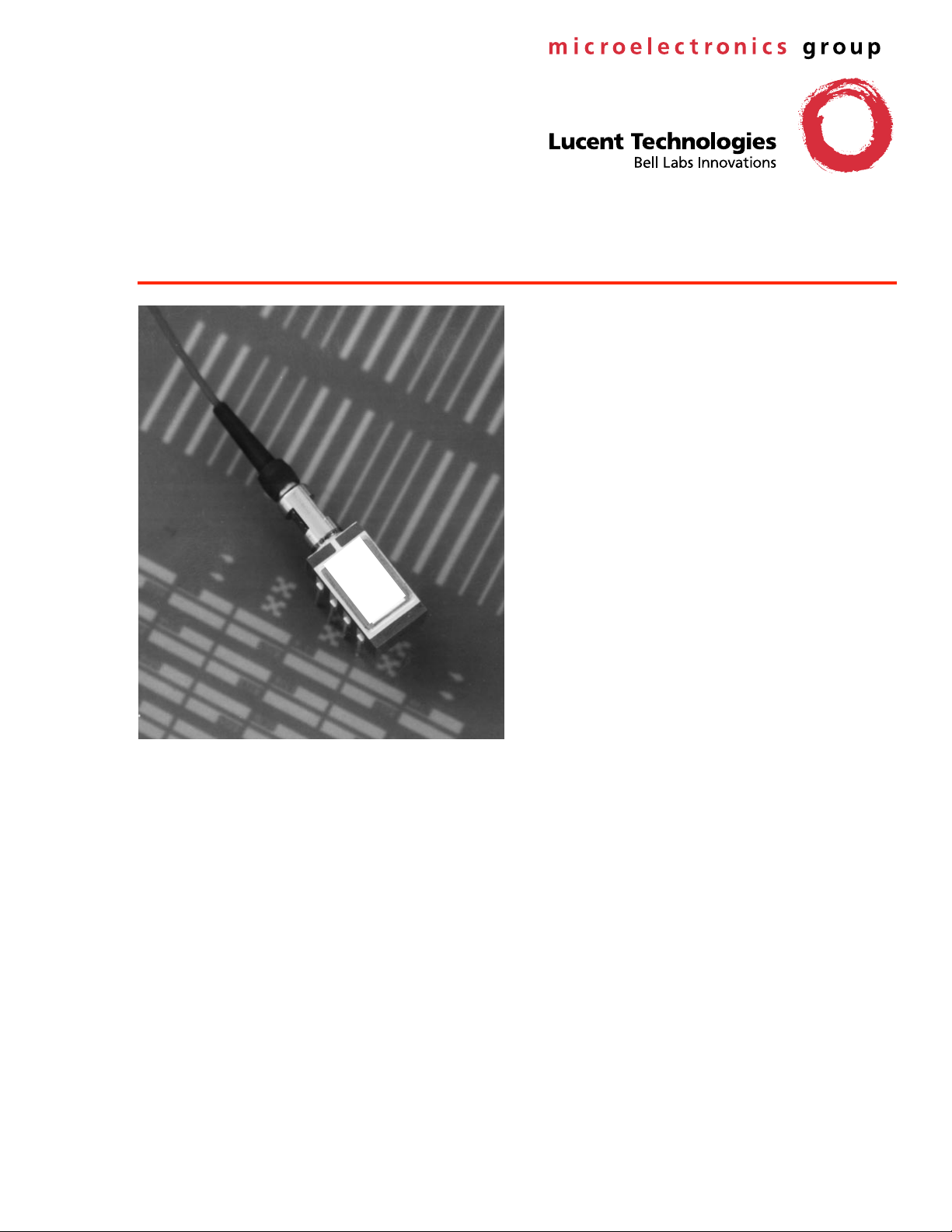
The low-profile D571-Type Laser Module is ideally suited for
short- and long-haul SONET and other high-speed digital
applications.
Features
■
Eight-pin package suitable for SONET/SDH
applications
■
Narrow linewidth, distributed-feedback, multiquantum-well (DFB-MQW), 1510 nm or 1550 nm laser
with single-mode fiber pigtail
■
Available in narrow and wide temperature ranges
■
No TEC required
■
High output power:
— Typical 2.0 mW peak power coupled into single-
mode fiber
— 1.0 mW devices are also available
Applications
■
Long-reach SONET OC-3/STM-1, OC-12/STM-4
systems
■
Telecommunications
■
Secure digital data systems
Benefits
■
Easily board mounted
■
Requires no lead bending
■
No additional heat sinks required
■
Pin compatible with industry-standard 14-pin laser
module
■
Highly efficient DFB-MQW laser structure allows
for lower threshold and drive currents , and reduced
power consumption
Description
The D571-T ype Uncooled Laser Module consists of a
laser diode coupled to a single-mode fiber pigtail.
The device is available in a standard, 8-pin configuration (see Figure 1 and/or Table 1) and is ideal for
long-reach (SONET) and other high-speed digital
applications.
The laser diode is a narrow linewidth (<1 nm) DFBMQW single-mode laser and an InGaAs PIN photodiode back-facet monitor in an epoxy-free, hermetically sealed package.
±
°
°
D571-Type Digital 1.5 µ m Uncooled DFB Advance Data Sheet
FastLight
Laser Module April 2000
Description
(continued)
The device characteristics listed in this document are
met at 2.0 mW output power. Higher- or lower-power
operation is possible. Under conditions of a fixed photodiode current, the change in optical output is typically
0.5 dB over an operating temperature range of
–40 ° C to +85 ° C.
This device incorporates the new Laser 2000 manufac-
turing process developed by the Optoelectronic unit of
Lucent Technologies Microelectronics Group. Laser
2000 is a low-cost platform that targets high-volume
manufacturing and tighter product distributions on all
optical subassemblies. The platform incorporates an
advanced optical design that is produced on a highly
automated production line. The Laser 2000 platform is
43 12
56 87
qualified for the central office and uncontrolled environments, and can be used for applications requiring high
performance and low cost.
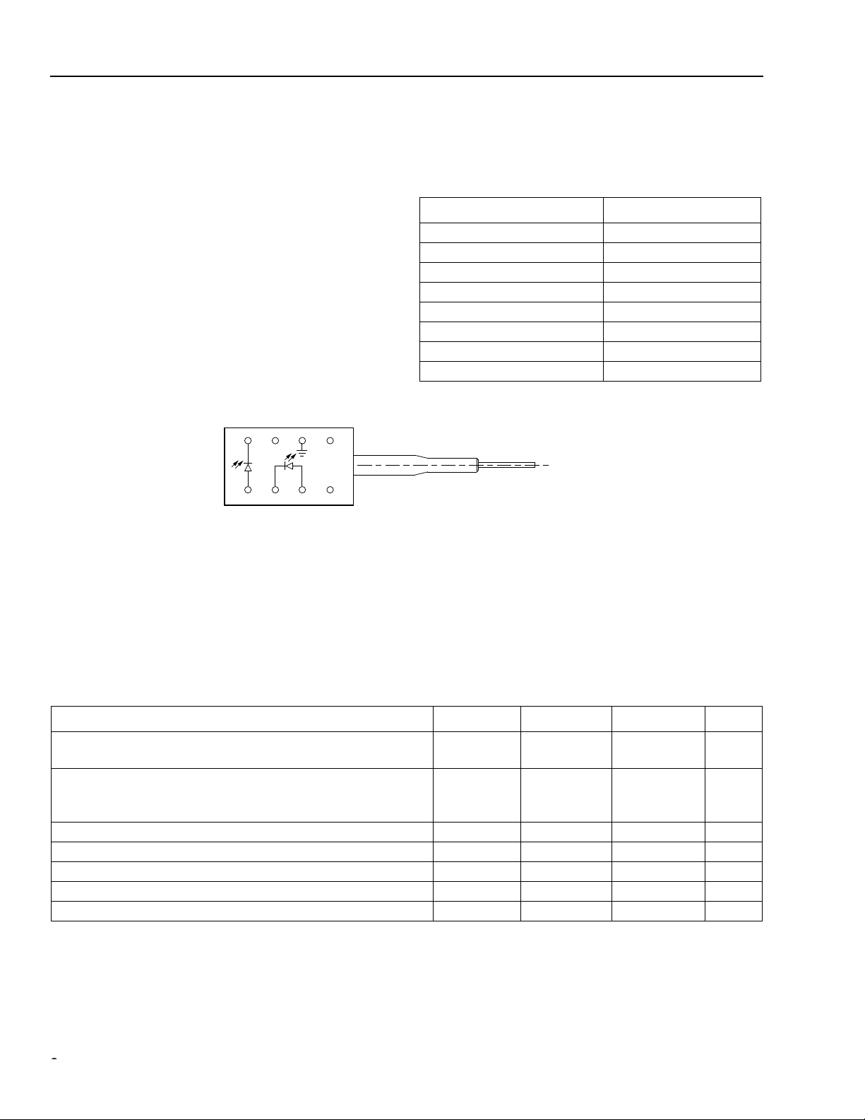
Table 1. Pin Descriptions
Pin Number Connection
1 NC/Reserved
2 Case ground
3 NC/Reserved
4 Photodiode cathode
5 Photodiode anode
6 Laser diode cathode
7 Laser diode anode
8 NC/Reserved
1-900 (C)
Figure 1. D571-Type Digital Uncooled DFB Flat-PAC Laser Module Schematic, Top View
Absolute Maximum Ratings
Stresses in excess of the absolute maximum ratings can cause permanent damage to the device. These are absolute stress ratings only. Functional operation of the device is not implied at these or any other conditions in excess
of those given in the operations sections of the data sheet. Exposure to absolute maximum ratings for extended
periods can adversely affect device reliability.
Parameter Symbol Min Max Unit
Maximum Peak Laser Drive Current or
Maximum Fiber Power*
Peak Reverse Laser Voltage:
Laser
Monitor
Monitor Forward Current I
Operating Case Temperature Range T
Storage Case Temperature Range T
Lead Soldering Temperature/Time —
Relative Humidity (noncondensing) RH — 85 %
* Rating varies with temperature.
P
I
V
V
OP
MAX
RL
RM
FD
C
stg
—
—
—
—
150
10
2
20
mA
mW
V
V
—2mA
–40 85
–40 85
C
C
— 260/10 ° C/s
22
Lucent Technologies Inc.

°
∆λ
µ
Ω
µ
Advance Data Sheet D571-Type Digital 1.5 µ m Uncooled DFB
April 2000
FastLight
Laser Module
Handling Precautions
CAUTION: This device is susceptible to damage as a result of electrostatic discharge (ESD). Take proper
precautions during both handling and testing. Follow guidelines such as JEDEC Publication
No. 108-A (Dec. 1988).
Although protection circuitry is designed into the device, take proper precautions to avoid exposure to ESD.
Electro-Optical Characteristics
Table 2. Electro-Optical Characteristics (over operating temperature range unless otherwise noted)
Parameter Symbol Test Conditions Min Typ Max Unit
Operating Temperature
Range
Optical Output Power* P
Threshold Current I
Modulation Current I
Slope Efficiency
‡
Center Wav elength
Center Wav elength
1510 nm codes
Spectral Width (–20 dB)
Side-mode Suppression
Ratio
Tracking Error TE I
Spontaneous Emission P
Rise/Fall Times t
Forward Voltage V
Input Impedance R — 3 — 8
Monitor Current I
Monitor Dark Current I
Wav elength Tempera-
ture Coefficient
* 1mW power option also available. See Table 4 for more information.
† BOL value; EOL = 80 mA.
‡ The slope efficiency is used to calculate the modulation current for a desired output power. This modulation current plus the threshold current
comprise the total operating current for the device.
§ V
= reverse voltage.
R
T — –40 — 85
F
TH
MOD
CW, P
CW, nominal — 2 — mW
T = 25 ° C
T = full range
T = –10 ° C to + 70 ° C
= 2.0 mW, T = 25 ° C
F
CW, I
MON
= constant,
5
2
2
15
7.5
—
—
—
—
—
15
60
50
35
60
†
T = full range
SE CW, P
λ
C
λ
C
SMSR CW, P
TH
, t
R
F
F
= 2.0 mW, T = 25 ° C 57 — 133 µ W/mA
P
F
= 2.0 mW, CW 1525 — 1570 nm
P
= 2.0 mW, CW 1500 — 1520 nm
F
P
F
= 2.0 mW, 622 Mbits/s — — 1 nm
= 2.0 mW 30 40 — dB
F
MON
= constant, CW –1.5 — 1.5 dB
I = (0.9) I
TH
10%—90% pulse
— — 100
— 0.25 0.5 ns
T = 25 ° C
F
MON
D
CW — 1.1 1.6 V
§
V
= 5 V 100 — 1000
R
§
R
V
= 5 V — 10 200 nA
— — — 0.09 0.12 nm/ ° C
C
mA
mA
mA
mA
mA
W
A
Lucent Technologies Inc.
3
 Loading...