

AGERE ATTL7557AAU, ATTL7556AAU Datasheet

Data Sheet
January 2000
L7556, L7557 Low-Power SLICs
with Battery Switch
Features
■ Auxiliary input for second battery, and internal
switch to enable its use to save power
■ Low active power (typical 125 mW during on-hook
transmission)
■ Supports meter pulse injection
■ Spare op amp for meter pulse filtering
■ –16 V to –60 V power supply operation
■ Distortion-free on-hook transmission
■ Convenient operating states:
— Forward powerup
— Disconnect (high impedance)
— 2-wire wink (zero loop voltage)
■ Adjustable supervision functions:
— Off-hook detector with longitudinal rejection
— Ground key detector
— Ring trip detector
■ Independent, adjustable, dc and ac parameters:
— dc feed resistance
— Loop current limit
— Termination impedance
Description
These electronic subscriber loop interface circuits
(SLICs) are optimized for low power consumption
while providing an extensive set of features.
The SLICs include an auxiliary battery input and a
built-in switch. In short-loop applications, they can be
used in high battery to present a high on-hook voltage, and then switched to low battery to reduce offhook power.
The SLICs also include a summing node for meter
pulse injection to 2.2 Vrms. A spare, uncommitted op
amp is included for meter pulse filtering.
The switched battery is applied to the power amplifiers of the device. There are two versions. The L7556
has the battery switch completely under processor
control. The L7557 can automatically switch to lower
battery when appropriate and includes hysteresis to
avoid frequent switching. To make the switch silent,
an external capacitor can be added to slow the transition.
The L7556 is suited for applications serving only
short loops, where a high on-hook voltage is required
for compatibility with preexisting standards.
■ Thermal protection
The L7557 is suited for applications where a full loop
range is needed, but low short-loop power is desired.
It is a much lower-cost solution than a switching regulator, and also occupies much less PCB area, needing only a battery filter capacitor and a diode for
implementation.
The device is available in a 32-pin PLCC package. It
is built by using a 90 V complementary bipolar integrated circuit (CBIC) process.

L7556, L7557 Low-Power SLICs
with Battery Switch
Data Sheet
January 2000
Table of Contents
Contents Page
Features ..................................................................... 1
Description ............................... ....... ............. ............. ..1
Pin Information ............................................................4
Functional Description.................................................6
Absolute Maximum Ratings ........................................6
Recommended Operating Conditions ................ ....... ..7
Electrical Characteristics .............................................7
Ring Trip Requirements.........................................11
Test Configurations .................................................. 12
Applications .............................................................. 14
Design Considerations ...........................................16
Characteristic Curves............................................. 17
dc Applications .......................................................20
Battery Feed.........................................................20
Switching the Battery............................................20
Overhead Voltage ........................................ .......21
Adjusting Overhead Voltage ................................21
Adjusting dc Feed Resistance.... ..........................22
Loop Range..........................................................22
Off-Hook Detection ..............................................22
Ring Trip Detection.............................................. 23
Ring Ground Detection........................................ 23
ac Design ...............................................................24
First-Generation Codecs ..................................... 24
Second-Generation Codecs................................ 24
Third-Generation Codecs.................................... 24
Selection Criteria................................................. 24
PCB Layout Information ............................................26
Outline Diagram.........................................................27
32-Pin PLCC....................................... ....... ...... .......27
Ordering Information..................................................28
Tables Page
Table 1. Pin Descriptions ............................................4
Table 2. Input State Coding ........................................6
Table 3. Supervision Coding .......................................6
Table 4. Power Supply ................................................7
Table 5. 2-Wire Port ....................................................8
Table 6. Analog Pin Characteristics ............................9
Table 7. Uncommitted Op Amp Characteristics ..........9
Table 8. ac Feed Characteristics ..............................10
Table 9. Logic Inputs and Outputs ............................ 11
Table 10. Parts List for Loop Start and Ground
Start Applications ............ ...... ....... ...... .......15
Table 11. 600 Ω Design Parameters .........................16
Figures Page
Figure 1. Functional Diagram .....................................3
Figure 2. Pin Diagram (PLCC Chip) ...........................4
Figure 3. Ring Trip Circuits .......................................11
Figure 4. Basic Test Circuit .......................................12
Figure 5. Longitudinal Balance .................................12
Figure 6. Longitudinal PSRR ....................................13
Figure 7. RFI Rejection .............................................13
Figure 8. Longitudinal Impedance ............................13
Figure 9. Metallic PSRR ...........................................13
Figure 10. ac Gains ..................................................13
Figure 11. Basic Loop Start Application Circuit
Using T7504 Type Codec ........................14
Figure 12. Ring Ground Detection Circuit .................14
Figure 13. Receive Gain and Hybrid Balance vs.
Frequency ...............................................17
Figure 14. Transmit Gain and Return Loss vs.
Frequency ...............................................17
Figure 15. Typical V
Figure 16. Typical V
Rejection .................................................17
Figure 17. Loop Closure Program Resistor
Selection .................... .................... ..........18
Figure 18. Ring Ground Detection Programming .....18
Figure 19. Loop Current vs. Loop Voltage ................18
Figure 20. Loop Current vs. Loop Resistance ..........18
Figure 21. Typical SLIC Power Dissipation vs.
Loop Resistance ......................................19
Figure 22. Power Derating ........................................19
Figure 23. Longitudinal Balance Resistor Mismatch
Requirements .......................................... 19
Figure 24. Longitudinal Balance vs. Protection
Resistor Mismatch ...................................19
Figure 25. Loop Current vs. Loop Voltage ................20
Figure 26. SLIC 2-Wire Output Stage .......................21
Figure 27. Equivalent Circuit for Adjusting the Over-
head Voltage ...........................................21
Figure 28. Equivalent Circuit for Adjusting the dc
Feed Resistance ......................................22
Figure 29. Adjusting Both Overhead Voltage and dc
Feed Resistance .....................................22
Figure 30. Off-Hook Detection Circuit
Applications ............... .............................. 22
Figure 31. Ring Trip Equivalent Circuit and
Equivalent Application .............................23
Figure 32. ac Equivalent Circuit Not Including Spare
Op Amp ...................................................25
Figure 33. ac Equivalent Circuit Including Spare
Op Amp ...................................................25
CC Power Supply Rejection .......17
BAT Power Supply
2 Lucent Technologies Inc.
Data Sheet
January 2000
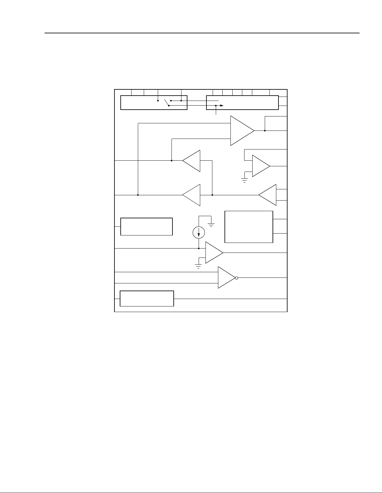
Description (continued)
L7556, L7557 Low-Power SLICs
with Battery Switch
PT
PR
DCR
LCTH
BS
BATTERY
SWITCH
dc RESISTANCE
ADJUST
LOOP CLOSURE DETECTOR
VBAT2
LBAT
BAT1
V
A = –4
A = 4
PROG
BGND
I
BS2
BS1
POWER CONDITIONING
& REFERENCE
VREG
AGND
VCC
CF1
CF2
DCOUT
+
1 V/8 mA
VITR
–
SN
SPARE
OP AMP
–
XMT
+
–
RCVN
+
RCVP
BATTERY FEED
STATE CONTROL
+
–
B0
B1
NLC
RTSP
RTSN
ICM
RING TRIP DETECTOR
RING GROUND
DETECTOR
Figure 1. Functional Diagram
+
NRDET
–
RGDET
12-2551.a (F)
Lucent Technologies Inc. 3
L7556, L7557 Low-Power SLICs
with Battery Switch
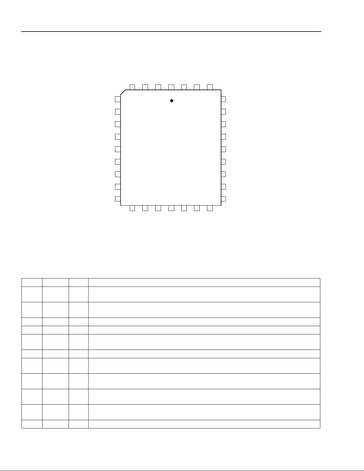
Pin Information
Data Sheet
January 2000
V
CC
RCVP
RCVN
LCTH
DCOUT
BAT1
V
PR
CF2
CF1
BAT
BS
NC
L
4 3 2 1 32 31
5
6
7
8
9
10
11
12
13
14 15
VITR
16 18 19 2017
ICM
BAT2
IPROG
V
32-PIN PLCC
B0
RGDET
BS1
AGND
BS2
AGND
NC
30
29 SN
28
27
26
25
24
23
22
21
DCR
XMT
B1
NLC
NRDET
RTSP
RTSN
PT
BGND
12-2548.q (F)
Figure 2. Pin Diagram (PLCC Chip)
Table 1. Pin Descriptions
Pin Symbol Type Description
1 VBAT2 — Auxiliary Battery Supply. Negative high-voltage battery, lower in magnitude than
BAT1, used to reduce power dissipation on short loops.
V
2 IPROG I Current-Limit Program Input. A resistor to DCOUT sets the dc current limit of the
device.
3 BS I Battery Switch. See Table 2 for description.
4 NC — No Connection (L7556 Only). Do not use as a tie point.
4 LBAT O Lower Battery in Use (L7557 Only). When high, this open-collector output indicates
the device has switched to V
BAT2. To use, connect a 100 k
resistor to VCC.
Ω
5 VCC — +5 V Power Supply.
6 RCVP I Receive ac Signal Input (Noninverting). This high-impedance input controls the ac
differential voltage on tip and ring.
7 RCVN I Receive ac Signal Input (Inverting). This high-impedance input controls the ac differ-
ential voltage on tip and ring.
8 LCTH I Loop Closure Threshold Input. Connect a resistor to DCOUT to set off-hook thresh-
old.
9 DCOUT O dc Output Voltage. This output is a voltage that is directly proportional to the absolute
value of the differential tip/ring current.
10 VBAT1 — Battery Supply. Negative high-voltage power supply, higher in magnitude than VBAT2.
4 Lucent Technologies Inc.

Data Sheet
January 2000
Pin Information (continued)
L7556, L7557 Low-Power SLICs
with Battery Switch
Table 1. Pin Descriptions
Pin Symbol Type Description
11 PR I/O Protected Ring. The output of the ring driver amplifier and input to loop sensing cir-
12 CF2 — Filter Capacitor 2. Connect a 0.1 µF capacitor from this pin to AGND.
13 CF1 — Filter Capacitor 1. Connect a 0.47 µF capacitor from this pin to pin CF2.
14 VITR O Transmit ac Output Voltage. This output is a voltage that is directly proportional to the
15 ICM I Common-Mode Current Sense. To program ring ground sense threshold, connect a
16 RGDET O Ring Ground Detect. When high, this open-collector output indicates the presence of
17 B0 I State Control Input. B0 and B1 determine the state of the SLIC. See Table 2.
18 AGND — Analog Signal Ground.
19 AGND — Analog Signal Ground.
20 DCR I dc Resistance for Low Loop Currents. Leave open for dc feed resistance of 115 Ω,
21 BGND — Battery Ground. Ground return for the battery supply.
22 PT I/O Protected Tip. The output of the tip driver amplifier and input to loop sensing circuitry.
23 RTSN I Ring Trip Sense Negative. Connect this pin to the ringing generator signal through a
24 RTSP I Ring Trip Sense Positive. Connect this pin to the ring relay and the ringer series resis-
25 NRDET O Ring T rip Detector Output. When low , this logic output indicates that ringing is tripped.
26 NLC O Loop Detector Output. When low, this logic output indicates an off-hook condition.
27 B1 I/O State Control Input. B0 and B1 determine the state of the SLIC. See Table 2. Pin B1
28 XMT O Transmit ac Output Voltage. The output of the uncommitted operational amplifier.
29 SN I Summing Node. The inverting input of the uncommitted operational amplifier. A resis-
30 NC — No Connection. Do not use as a tie point.
31 BS2 — Battery Switch Slowdown. A 0.1 µF capacitor from BS1 to BS2 will ramp the battery
32 BS1 — Battery Switch Slowdown. A 0.1 µF capacitor from BS1 to BS2 will ramp the battery
(continued)
cuitry. Connect to loop through overvoltage protection.
differential tip/ring current.
resistor to V
can be left unconnected.
a ring ground. To use, connect a 100 kΩ resistor to V
or short to DCOUT for 615 Ω. Intermediate values can be set by a simple resistor
divider from DCOUT to ground with the tap at DCR.
Connect to loop through overvoltage protection.
high-value resist or.
tor through a high-value resistor.
has a 40 kΩ pull-up. It goes low in the event of thermal shutdown.
tor or network to XMT sets the gain.
switch transition for applications requiring quiet transition. If not needed, the pin can be
left open.
switch transition for applications requiring quiet transition. If not needed, the pin can be
left open.
CC and connect a capacitor to AGND to filter 50/60 Hz. If unused, the pin
CC.
Lucent Technologies Inc. 5

L7556, L7557 Low-Power SLICs
with Battery Switch
Data Sheet
January 2000
Functional Description
Table 2. Input State Coding
B0 B1 BS State/Definition
1 1 1 Powerup, Forward Battery. Normal talk and battery feed state. Pin PT is positive with respect
to PR. On-hook transmission is enabled. V
1 1 0 Powerup, Forward Battery. Normal talk and battery feed state. Pin PT is positive with respect
to PR. On-hook transmission is enabled.
For the L7556 only, V
BAT2 is applied to tip/ring drive amplifiers.
For the L7557 only, the device compares the magnitude of V
maintain proper loop current. Then the device automatically applies V
plifiers when possible, not affecting the desired dc template.
1 0 1 2-Wire Wink. Pins PT and PR are put at the same potential (near ground). VBAT1 is applied to
entire circuit.
0 0 1 Disconnect. The tip and ring amplifiers are turned off, and the SLIC goes to a high-impedance
state (>100 kΩ).V
BAT1 is applied to entire circuit.
Table 3. Supervision Coding
Pin NLC Pin NRDET Pin RGDET
0 = off-hook
1 = on-hook
0 = ring trip
1 = no ring trip
BAT1 is applied to entire circuit.
BAT2 to the voltage necessary to
BAT2 to tip/ring drive am-
1 = ring ground
0 = no ring ground
Absolute Maximum Ratings (TA = 25 °C)
Stresses in excess of the Absolute Maximum Ratings can cause permanent damage to the device. These are
absolute stress ratings only. Functional operation of the device is not implied at these or any other conditions in
excess of those given in the operational sections of the data sheet. Exposure to Absolute Maximum Ratings for
extended periods can adversely affect device reliability
Parameter Symbol Value Unit
5 V Power Supply VCC 7.0 V
Battery (Talking) Supply VBAT1 –63 V
Auxiliary Battery Supply VBAT2 –63 V
Logic Input Voltage — –0.5 to +7.0 V
Analog Input Voltage — –7.0 to +7.0 V
Maximum Junction Temperature TJ 165 °C
Storage Temperature Range Tstg –40 to +125 °C
Relative Humidity Range RH 5 to 95 %
Ground Potential Difference (BGND to AGND) — ±3 V
PT or PR Fault Voltage (dc) VPT, VPR (VBAT1 – 5) to +3 V
PT or PR Fault Voltage (10 x 1000 µs) VPT, VPR (VBAT1 – 15) to +15 V
Current into Ring Trip Inputs IRTSP, IRTSN ±240 µA
Note: The IC can be damaged unless all ground connections are applied before, and removed after, all other connections. Furthermore, when
powering the device, the user must guarantee that no external potential creates a voltage on any pin of the device that exceeds the
device ratings. Some of the known examples of conditions that cause such potentials during powerup are the following:
1. An inductor connected to tip and ring can force an overvoltage on V
2. Inductance in the V
BAT
leads could resonate with the V
.
BAT through the protection devices if the VBA T connections chatter.
BAT filter capacitors to cause a destructive overvoltage.
6 Lucent Technologies Inc.

Data Sheet
January 2000
L7556, L7557 Low-Power SLICs
with Battery Switch
Recommended Operating Conditions
Parameter Min Typ Max Unit
Ambient Temperature –40 — 85 °C
VCC Supply Voltage 4.75 5.0 5.25 V
VBAT1 Supply Voltage –24 –48 –60 V
VBAT2 Supply Voltage –16 –28 VBAT1 V
Loop Closure Threshold-detection Programming Range — 10 ILIM mA
dc Loop Current-limit Program mi ng Rang e 5 22 45 mA
On- and Off-hook 2-wire Signal Level — 1 2.2 Vrms
ac Termination Impedance Pr og rammi ng Rang e 150 600 1300 Ω
Electrical Characteristics
Minimum and maximum values are testing requirements. Typical values are characteristic of the device and are
the result of engineering evaluations. Typical values are for information purposes only and are not part of the test-
ing requirements. Minimum and maximum values apply across the entire temperature range (–40 °C to +85 °C)
and the entire battery range unless otherwise specified. Typical is defined as 25 °C, V
BAT2 = –48 V, and ILIM= 40 mA. Positive currents flow into the device. Test circuit is Figure 4 unless noted.
V
CC = 5.0 V, VBAT1 = –48 V,
Table 4. Power Supply
Parameter Min Typ Max Unit
Power Supply—Powerup, No Loop Current:
CC
I
BAT (VBAT = –48 V)
I
Power Dissipation (V
BAT = –48 V)
—
—
—
2.8
–2.3
125
—
—
155
Power Supply Rejection 500 Hz to 3 kHz (See Figures 5, 6, 15, and 16.)1:
CC
V
VBAT
35
45
—
—
—
—
Thermal Protection Shutdown (Tjc) — 175 — °C
Thermal Resistance, Junction to Ambient (
1. This parameter is not tested in production. It is guaranteed by design and device characterization.
JA) — 60 — °C/W
θ
mA
mA
mW
dB
dB
Lucent Technologies Inc. 7

L7556, L7557 Low-Power SLICs
with Battery Switch
Electrical Characteristics (continued)
Table 5. 2-Wire Port
Parameter Min Typ Max Unit
Tip or Ring Drive Current:
= dc + Longitudinal + Signal Currents
Signal Current 15
Longitudinal Current Capability per Wire
1
65
8.5
— —
— —
15 —
Data Sheet
January 2000
mA
mArms
mArms
dc Loop Current Limit2:
LOOP = 100
R
Ω
Programmability Range
Accuracy (20 mA < I
LIM < 40 mA)
—
5
—
ILIM
—
—
—
45
±12
mA
mA
Powerup Open Loop Voltage Levels (includes external diode):
Differential Voltag e
|VBAT + 8.4| |VBAT + 7.9| |VBAT + 7.4| V
Disconnect State:
PT Resistance (V
PR Resistance (V
BAT < VPT < 0 V)
BAT < VPR < 0 V)
100
100
143
133
—
—
k
k
Ground Start State:
PT Resistance
100
143 —
k
dc Feed Resistance (for ILOOP below regulation level) 95 115 135 Ω
Loop Resistance Range (–3.17 dBm overload into 600 Ω; not
including protection):
LOOP = 20 mA at VBAT2 = –48 V
I
LOOP = 20 mA at VBAT2 = –24 V
I
Longitudinal to Metallic Balance—
4
Figure 6.)
:
50 Hz to 1 kHz
1 kHz to 3 kHz
IEEE
3
Std. 455 (See
1885
685
64
60
—
—
75
70
—
—
—
—
dB
dB
Metallic to Longitudinal Balance:
200 Hz to 4 kHz
46
— —
dB
RFI Rejection (See Figure 7.)5:
0.5 Vrms, 50 Ω Source, 30% AM Mod 1 kHz
500 kHz to 100 MHz
—
–55 –45 dBV
%
Ω
Ω
Ω
Ω
Ω
1.The longitudinal current is independent of dc loop current.
2.Current-limit I
begins (see Figure 19). Select R
IEEE
3.
4.Longitudinal balance of circuit card will depend on loop series resistance matching (see Figure 23 and Figure 24).
5.This parameter is not tested in production. It is guaranteed by design and device characterization.
LIM is programmed by a resistor, RPROG, from pin IPROG to DCOUT. ILIM is specified at the loop resistance where current limiting
is a registered trademark of The Institute of Electrical and Electronics Engineers, Inc.
PROG (k
) =1.67 x ILIM (mA).
Ω
8 Lucent Technologies Inc.

Data Sheet
January 2000
Electrical Characteristics (continued)
Table 6. Analog Pin Characteristics
Parameter Min Typ Max Unit
Differential PT/PR Current Sense (DCOUT):
Gain (PT/PR to DCOUT)
L7556, L7557 Low-Power SLICs
with Battery Switch
–123 –125 –127 V/A
Loop Closure Detector Threshold1:
Programming Accu racy
— — ±20 %
Ring Ground Detector Threshold2:
ICM = 154 k
R
Ω
Programming Accu racy
3
—
—
6
10
±25
Ring Trip Comparator:
Input Offset Voltage
— — ±10 mV
RCVN, RCVP:
Input Bias Current
1. Loop closure threshold is programmed by resistor RLCTH from pin LCTH to pin DCOUT.
2. Ring ground threshold is programmed by resistor RICM2 from pin ICM to V
— –0.2 –1 µA
CC.
Table 7. Uncommitted Op Amp Characteristics
Parameter Min Typ Max Unit
Input Offset Voltage
Input Offset Current
Input Bias Current
Differential Input Resistance
Output Voltage Swing (RL = 10 kΩ)
Output Resistance (A
VCL = 1)
—
—
—
—
—
—
±5
±10
200
1.5
±3.5
2.0
—
—
—
—
—
—
Vpk
Small Signal GBW — 700 — kHz
k
Ω
%
mV
nA
nA
M
Ω
Ω
Lucent Technologies Inc. 9
 Loading...