

AGERE ATTL7554AP Datasheet

Data Sheet
March 1997
L7554 Low-Power SLIC
Features
■
Low active power (typical 165 mW during on-hook
transmission)
■
Sleep state for low idle power (76 mW)
■
Quiet Tip/Ring polarity reversal
■
Supports meter pulse injection
■
Spare op amp for meter pulse filtering
■
–24 V to –72 V power supply operation
■
Distortion-free on-hook transmission
■
Convenient operating states:
— Forward powerup
— Polarity reversal powerup
— Forward low-power scan
— Polarity reversal low-power scan
— Ground start
— Disconnect (high impedance)
■
Adjustable supervision functions:
— Off-hook detector with longitudinal rejection
— Ground key detector
— Ring trip detector
Description
This electronic subscriber loop interface circuit
(SLIC) is optimized for low-power consumption while
providing an extensive set of features.
Quiet polarity reversal is possible because the ac
path is uninterrupted during transition.
The L7554 includes the ground start state and a
summing node for meter pulse injection to 2.2 Vrms.
A spare, uncommitted op amp is included for meter
pulse filtering.
The device is being offered in two versions, based
upon maximum battery. The L7554AP is guaranteed
to –60 V, and the L7554BP is guaranteed to –72 V.
The device is available in a 44-pin PLCC package. It
is built by using a 90 V complementary bipolar
(CBIC) process.
■
Independent, adjustable, dc and ac parameters:
— dc feed resistance
— Loop current limit
— Termination impedance
■
Thermal protection

L7554 Low-Power SLIC
Data Sheet
March 1997
Table of Contents
Content Page
Features .................................................................................................................................................................. 1
Description ............................................................................................................................................................... 1
Pin Information ......................................................................................................................................................... 4
Functional Description.............................................................................................................................................. 6
Absolute Maximum Ratings ..................................................................................................................................... 6
Recommended Operating Conditions ..................................................................................................................... 7
Electrical Characteristics......................................................................................................................................... 7
Ring Trip Requirements..................................................................................................................................... 11
Test Configurations ............................................................................................................................................... 12
Applications ........................................................................................................................................................... 14
Design Considerations ....................................................................................................................................... 16
Characteristic Curves......................................................................................................................................... 17
dc Applications ................................................................................................................................................... 20
Battery Feed.................................................................................................................................................... 20
Overhead Voltage .......................................................................................................................................... 20
Adjusting Overhead Voltage ........................................................................................................................... 21
Adjusting dc Feed Resistance......................................................................................................................... 22
Adjusting Overhead Voltage and dc Feed Resistance Simultaneously .......................................................... 22
Loop Range..................................................................................................................................................... 22
Off-Hook Detection ......................................................................................................................................... 22
Ring Trip Detection......................................................................................................................................... 23
Ring Ground Detection................................................................................................................................... 23
ac Design ........................................................................................................................................................... 24
First-Generation Codecs.................................................................................................................................. 24
Second-Generation Codecs ............................................................................................................................ 24
Third-Generation Codecs ................................................................................................................................ 24
Selection Criteria ............................................................................................................................................. 24
PCB Layout Information ......................................................................................................................................... 26
Outline Diagram...................................................................................................................................................... 27
44-Pin PLCC....................................................................................................................................................... 27
Ordering Information........................................................................................................................................... 28
2 Lucent Technologies Inc.
Data Sheet
March 1997
L7554 Low-Power SLIC
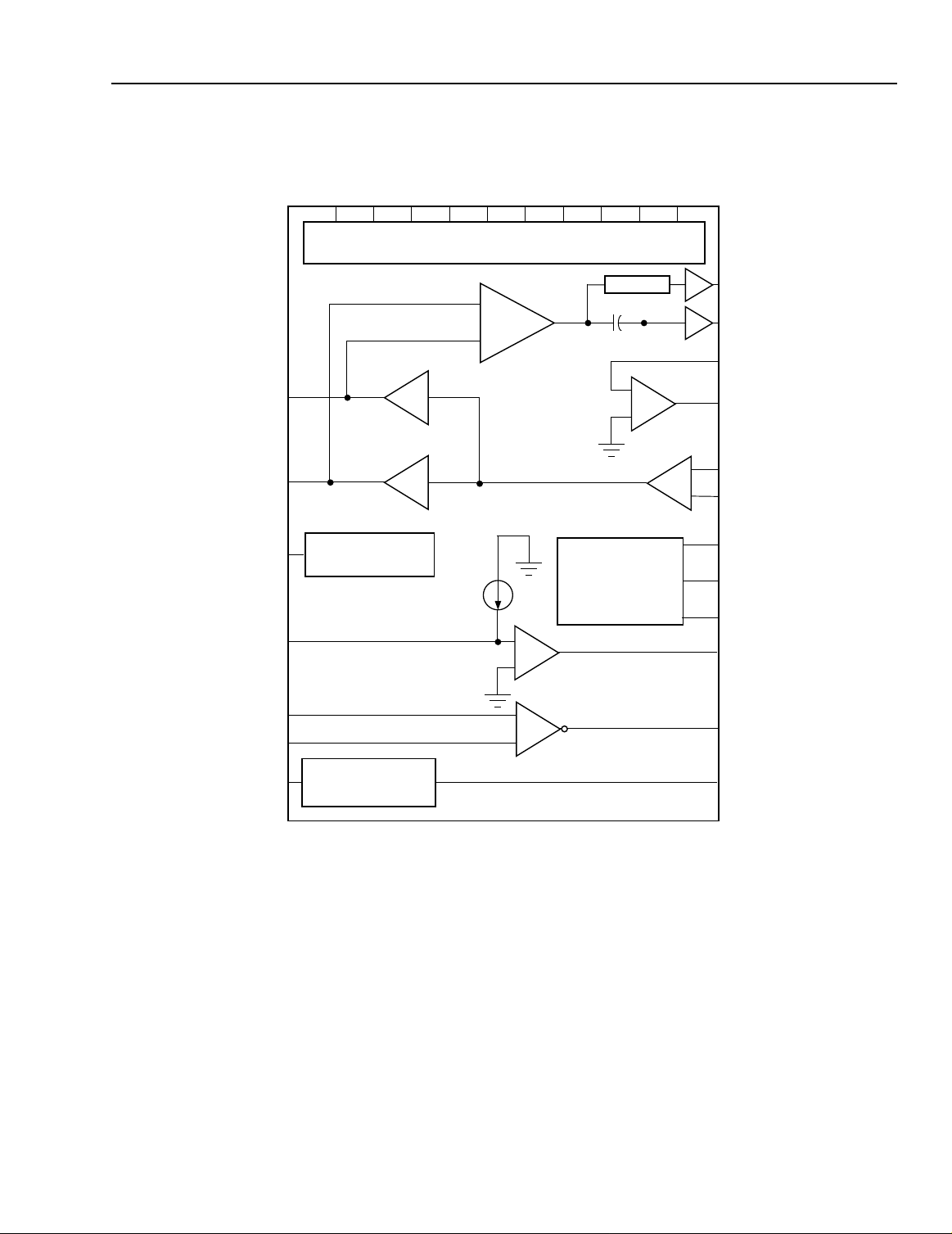
Description
(continued)
PT
PR
DCR
LCTH
IPROG
dc RESISTANCE
ADJUST
LOOP CLOSURE DETECTOR
VBAT
VCC
POWER CONDITIONING & REFERENCE
A = 4
A = –4
BGND
VREG
–
–1 V/24 mA
+
+
–
AGND
V
CF2
CF1
RECTIFIER
TX TXI
0.1 µF
C
EXTERNAL
SPARE
OP AMP
BATTERY FEED
STATE CONTROL
–
+
FB1
FB2
DCOUT
3
VITR
9.6
SN
XMT
RCVN
–
1
RCVP
+
B0
B1
B2
NLC
RTSP
RTSN
ICM
RING TRIP DETECTOR
RING GROUND
DETECTOR
+
NRDET
–
RGDET
12-2569 (C)
Figure 1. Functional Diagram
Lucent Technologies Inc. 3
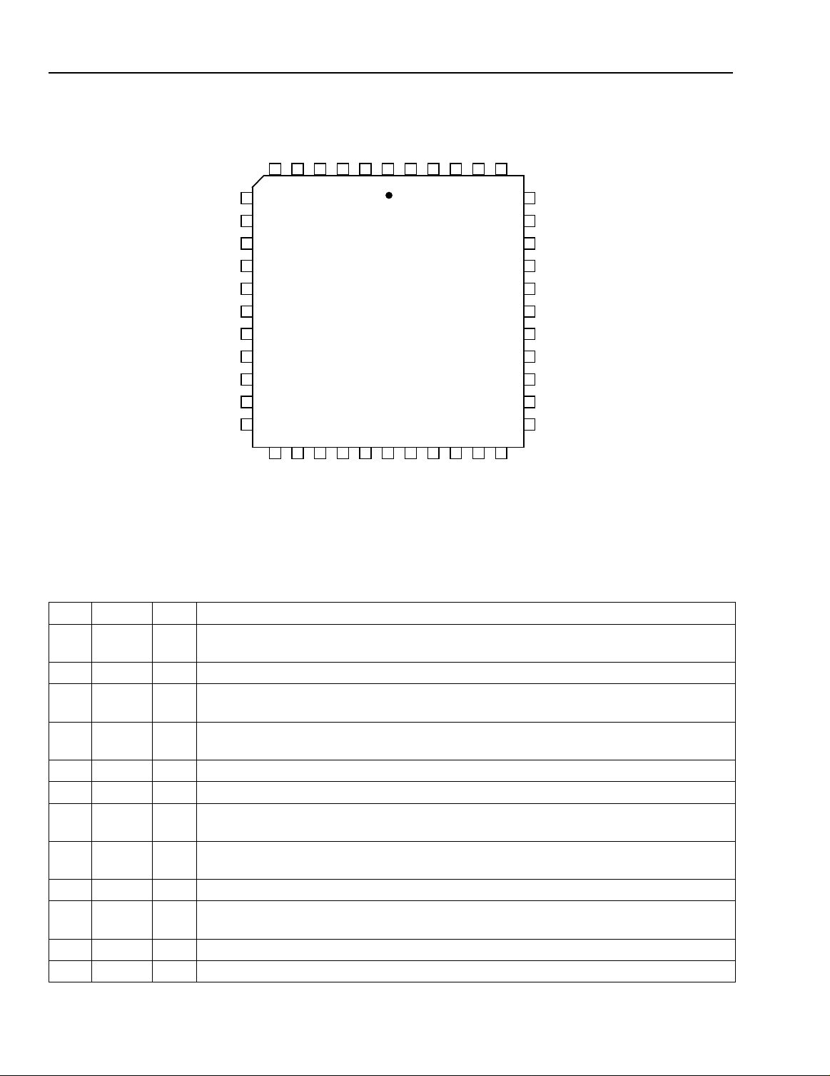
L7554 Low-Power SLIC
Pin Information
RCVP
RCVN
LCTH
V
DCOUT
V
V
TXI
REG
CC
BAT
PR
6 4 3 2 1 44434241405
7
8
9
10
11
12
13
14
15
16
17
18 20 21 22 23 24 25 26 27 2819
PROG
I
L7554
FB2
39
38
37
36
35
34
33
32
31
30
29
Data Sheet
March 1997
FB1
SN
XMT
B1
B2
NLC
NRDET
RTSP
RTSN
PT
VTX
CF2
CF1
VITR
CM
I
GDET
R
B0
AGND
AGND
DCR
Figure 2. Pin Diagram (PLCC Chip)
Table 1. Pin Descriptions
Pin Symbol Type Description
3
PROG
I
I
Current-Limit Program Input.
A resistor to DCOUT sets the dc current limit of the
device.
8 V
CC
9 RCVP I
+5 V Power Supply.
Receive ac Signal Input (Noninverting).
This high-impedance input controls the ac
—
differential voltage on Tip and Ring.
10 RCVN I
Receive ac Signal Input (Inverting).
This high-impedance input controls the ac differen-
tial voltage on Tip and Ring.
11 TXI —
12
LCTH I
13 V
REG
14 DCOUT O
ac/dc Separation.
Loop Closure Threshold Input.
I
Regulated Negative dc Battery Voltage.
Otherwise, connect to V
dc Output Voltage.
Connect a 0.1 µF capacitor from this pin to VTX
Connect a resistor to DCOUT to set off-hook threshold.
Can be connected to an external regulator.
BAT
.
This output is a voltage that is directly proportional to the absolute
value of the differential Tip/Ring current.
15 V
BAT
16 PR I/O
Battery Supply.
Protected Ring.
Negative high-voltage power supply.
The output of the ring driver amplifier and input to loop sensing circuitry.
—
Connect to loop through overvoltage protection.
18 CF2 —
19 CF1 —
Filter Capacitor 2.
Filter Capacitor 1.
Connect a 0.1 µF capacitor from this pin to AGND.
Connect a 0.47 µF capacitor from this pin to pin CF2.
BGND
12-2571 (C)
.
4 Lucent Technologies Inc.

Data Sheet
March 1997
L7554 Low-Power SLIC
Pin Information
Table 1. Pin Descriptions (continued)
Pin Symbol Type Description
20 VITR O
21 I
22 R
23 B0 I
24 AGND —
25 AGND —
26 DCR I
27 BGND —
29 VTX O This output is a voltage that is directly proportional to the differential Tip/Ring current.
30 PT I/O
31 RTSN I
32 RTSP I
33 NRDET O
34 NLC O
35 B2 I
36 B1 I/O
37 XMT O
38 SN I
39 FB1 I
40 FB2 I
CM
GDET
(continued)
Transmit ac Output Voltage.
differential ac Tip/Ring current.
I
Common-Mode Current Sense.
resistor to VCC and connect a capacitor to AGND to filter 50/60 Hz. If unused, the pin can
be left unconnected.
O
Ring Ground Detect.
ring ground. To use, connect a 100 kΩ resistor to VCC.
State Control Input.
Analog Signal Ground
Analog Signal Ground.
dc Resistance for Low Loop Currents.
short to DCOUT for 618 Ω. Intermediate values can be set by a simple resistor divider
from DCOUT to ground with the tap at DCR.
Battery Ground.
Protected Tip
loop through overvoltage protection.
Ring Trip Sense Negative
high-value resistor.
Ring Trip Sense Positive
through a high-value resistor.
Ring Trip Detector Output
Loop Detector Output
State Control Input
State Control Input
Transmit ac Output Voltage
Summing Node
or network to XMT sets the gain.
Forward Battery Slowdown.
AGND will ramp the polarity reversal transition for added flexibility in applications requiring
quiet polarity reversal. If not needed, the pin can be left open.
Forward Battery Slowdown.
AGND will ramp the polarity reversal transition for added flexibility in applications requiring
quiet polarity reversal. If not needed, the pin can be left open.
. The output of the tip driver amplifier and input to loop sensing. Connect to
When high, this open-collector output indicates the presence of a
B0, B1, and B2 determine the state of the SLIC. See Table 2.
Ground return for the battery supply.
. B0, B1, and B2 determine the state of the SLIC. See Table 2.
. B0, B1, and B2 determine the state of the SLIC. See Table 2.
. The inverting input of the uncommitted operational amplifier. A resistor
This output is a voltage that is directly proportional to the
To program ring ground sense threshold, connect a
.
Leave open for dc feed resistance of 118 Ω, or
. Connect this pin to the ringing generator signal through a
. Connect this pin to the ring rela y and the ringer series resistor
. When low, this logic output indicates that ringing is tripped.
. When low, this logic output indicates an off-hook condition.
. The output of the uncommitted operational amplifier.
A 0.1 µF capacitor from FB1 to AGND and from FB2 to
A 0.1 µF capacitor from FB2 to AGND and from FB1 to
Lucent Technologies Inc. 5

L7554 Low-Power SLIC
Functional Description
Table 2. Input State Coding
B0 B1 B2 State/Definition
1 1 1
1 1 0
0 1 1
0 1 0
0 0 1
0 0 0
Table 3. Supervision Coding
Powerup, Forward Battery.
Normal talk and battery feed state. Pin PT is positive with respect to
PR. On-hook transmission is enabled.
Powerup, Reverse Battery.
Normal talk and battery feed state. Pin PR is positive with respect to
PT. On-hook transmission is enabled.
Ground Start.
Tip drive amplifier is turned off. The device presents a high-impedance (>100 kΩ)
to the PT pin and a current-limited battery to the PR pin. Output pin RGDET indicates current flowing in the ring lead.
Low-Power Scan, Reverse Battery.
Except for off-hook supervision, all circuits are shut down to
conserve power. Pin PR is positive with respect to PT. On-hook transmission is disabled.
Low-Power Scan, Forward Battery.
Except for off-hook supervision, all circuits are shut down to
conserve power. Pin PT is positive with respect to PR. On-hook transmission is disabled.
Disconnect.
The Tip and Ring amplifiers are turned off and the SLIC goes to a high-impedance
state (>100 kΩ).
Data Sheet
March 1997
Pin NLC Pin NRDET Pin RGDET
0 = off-hook
1 = on-hook
Absolute Maximum Ratings
0 = ring trip
1 = no ring trip
(TA = 25 °C)
1 = ring ground
0 = no ring ground
Stresses in excess of the absolute maximum ratings can cause permanent damage to the device. These are absolute stress ratings only. Functional operation of the device is not implied at these or any other conditions in excess
of those given in the operational sections of the data sheet. Exposure to absolute maximum ratings for extended
periods can adversely affect device reliability.
Parameter Symbol Value Unit
5 V Power Supply V
Battery (Talking) Supply V
CC
BAT
7.0 V
–75 V
Logic Input Voltage — –0.5 to +7.0 V
Analog Input Voltage — –7.0 to +7.0 V
RTSP
stg
, I
J
H
PR
PR
RTSN
165
–40 to +125
5 to 95 %
±
3 V
(V
BAT
– 5) to +3 V
(V
BAT
– 15) to +15 V
±
240
°
°
µA
C
C
Maximum Junction Temperature T
Storage Temperature Range T
Relative Humidity Range R
Ground Potential Difference (BGND to AGND) —
PT or PR Fault Voltage (dc) VPT, V
PT or PR Fault Voltage (10 x 1000 µs) VPT, V
Current into Ring Trip Inputs I
Note: The IC can be damaged unless all ground connections are applied before, and remov ed after, all other connections. Furthermore, when
powering the device, the user must guarantee that no external potential creates a voltage on any pin of the device that exceeds the
device ratings. Some of the known examples of conditions that cause such potentials during powerup are the following: 1) an inductor
connected to Tip and Ring can force an overvoltage on V
inductance in the V
BAT
lead could resonate with the V
BAT
through the protection devices if the V
BAT
filter capacitor to cause a destructive overvoltage.
BAT
connection chatters, and 2)
6 Lucent Technologies Inc.

Data Sheet
March 1997
L7554 Low-Power SLIC
Recommended Operating Conditions
Parameter Min Typ Max Unit
Ambient Temperature –40 — 85 °C
VCC Supply Voltage 4.75 5.0 5.25 V
VBAT Supply Voltage:
L7554AP
L7554BP
Loop Closure Threshold-detection Programming Range — 10 ILIM mA
dc Loop Current-limit Programming Range 5 40 45 mA
On- and Off-hook 2-wire Signal Level — 1 2.2 Vrms
ac Termination Impedance Programming Range 150 600 1300 Ω
–24
–24
–40
–48
–60
–72
V
V
Electrical Characteristics
Minimum and maximum values are testing requirements. Typical values are characteristic of the device and are the
result of engineering evaluations. Typical values are for information purposes only and are not part of the testing
requirements. Minimum and maximum values apply across the entire temperature range (–40 °C to +85 °C) and
the entire battery range unless otherwise specified. Typical is defined as 25 °C, VCC = 5.0 V, VBAT = –48 V, and
ILIM = 40 mA. Positive currents flow into the device. Test circuit is Figure 4 unless noted.
Table 4. Power Supply
Parameter Min Typ Max Unit
Power Supply—Powerup, No Loop Current
ICC
IBAT (VBAT = –48 V)
Power Dissipation (VBAT = –48 V)
Power Supply—Low-Power Scan, Forward Bat, No Loop
Current
ICC
IBAT (VBAT = –48 V)
Power Dissipation (VBAT = –48 V)
Power Supply Rejection 500 Hz to 3 kHz
(See Figures 5, 6, 15, and 16.)
VCC
VBAT
Thermal Protection Shutdown (Tjc) — 175 — °C
Thermal Resistance, Junction to Ambient (θJA) — 47 — °C/W
1. This parameter is not tested in production. It is guaranteed by design and device characterization.
1
—
—
—
—
—
—
35
45
4.1
–3.0
165
2.7
–1.4
82
—
—
4.8
–3.5
191
3.7
–1.7
100
—
—
mA
mA
mW
mA
mA
mW
dB
dB
Lucent Technologies Inc. 7

L7554 Low-Power SLIC
Data Sheet
March 1997
Electrical Characteristics (continued)
Table 5. 2-Wire Port
Parameter Min Typ Max Unit
Tip or Ring Drive Current
= dc + Longitudinal + Signal Currents 65
Signal Current 15
Longitudinal Current Capability per Wire
dc Loop Current Limit
2
RLOOP = 100 Ω
Programmability Range
Accuracy (20 mA < ILIM < 40 mA)
1
8.5
—
5
—
Powerup Open Loop Voltage Levels
Common-mode Voltage
—
Differential Voltage:
VBAT = –48 V, Temperature = 25 °C
VBAT = –72 V, Temperature = 85 °C (L7554BP)
|VBAT + 7.0|
|VBAT + 10.0|
Disconnect State
PT Resistance (VBAT < VPT < 0 V)
PR Resistance (VBAT < VPR < 0 V)
100
100
Ground Start State
PT Resistance 100
dc Feed Resistance (for ILOOP below regulation level) 90 113 133 Ω
Loop Resistance Range (–3.17 dBm overload into
600 Ω; not including protection)
ILOOP = 20 mA at VBAT = –48 V
LOOP = 20 mA at VBAT = –24 V
I
Longitudinal to Metallic Balance—
(See Figure 7.)
4
50 Hz to 1 kHz
1 kHz to 3 kHz
IEEE
3
Std. 455
1900
700
64
60
Metallic to Longitudinal Balance
200 Hz to 4 kHz 46
RFI Rejection (See Figure 8.)
5
0.5 Vrms, 50 Ω Source, 30% AM Mod. 1 kHz
500 kHz to 100 MHz
—
— —
— —
15 —
ILIM
—
—
VBAT/2
|VBAT + 6.5|
|VBAT + 6.8|
143
133
—
45
±12
—
|VBAT + 6.0|
—
—
—
143 —
—
—
75
70
—
—
—
—
— —
–55 –45 dBV
mArms
mArms
mA
mA
mA
%
V
V
V
kΩ
kΩ
kΩ
Ω
Ω
dB
dB
dB
1. The longitudinal current is independent of dc loop current.
2. Current-limit ILIM is programmed by a resistor , RPROG, from pin IPR OG to DCOUT. ILIM is specified at the loop resistance where current limiting
begins (see Figure 25). Select RPROG (kΩ) = 1.67 x ILIM (mA).
3.
IEEE
is a registered trademark of The Institute of Electrical and Electronics Engineers, Inc.
4. Longitudinal balance of circuit card will depend on loop series resistance matching (see Figures 23 and 24).
5. This parameter is not tested in production. It is guaranteed by design and device characterization.
8 Lucent Technologies Inc.

Data Sheet
March 1997
L7554 Low-Power SLIC
Electrical Characteristics (continued)
Table 6. Analog Pin Characteristics
Parameter Min Typ Max Unit
Differential PT/PR Current Sense (DCOUT)
Gain (PT/PR to DCOUT)
Offset Voltage @ ILOOP = 0, VBAT = –48 V
Loop Closure Detector Threshold
1
Programming Accuracy
Ring Ground Detector Threshold
2
RICM = 83 kΩ
Programming Accuracy
Ring Trip Comparator
Input Offset Voltage — — ±10 mV
RCVN, RCVP
Input Bias Current — –0.2 –1 µA
1. Loop closure threshold is programmed by resistor RLCTH from pin LCTH to pin DCOUT.
2. Ring ground threshold is programmed by resistor RICM2 from pin ICM to VCC.
–119
–200
–125
—
–127
200
— — ±20 %
3
—
—
6
10
±25
V/A
mV
kΩ
%
Table 7. Uncommitted Op Amp Characteristics
Parameter Min Typ Max Unit
Input Offset Voltage
Input Offset Current
Input Bias Current
Differential Input Resistance
Output Voltage Swing (RL = 10 kΩ)
Output Resistance (AVCL = 1)
—
—
—
—
—
—
±5
±10
200
1.5
±3.5
2.0
—
—
—
—
—
—
mV
MΩ
Vpk
Small Signal GBW — 700 — kHz
nA
nA
Ω
Lucent Technologies Inc. 9
 Loading...