

AGERE A371-22FD, A371-22BD, A371-22AD, A371-20GS, A371-20FS Datasheet
...
™
Data Sheet
January 1999
A371-Type Analog Uncooled Isolated
DFB
■
■
■
■
■
FastLight
Laser Module
No thermoelectric cooler required
Single- and double-isolated versions available
High output power: typically 2.0 mW peak power
coupled into single-mode fiber
Hermetically sealed active components
Internal back-facet monitor
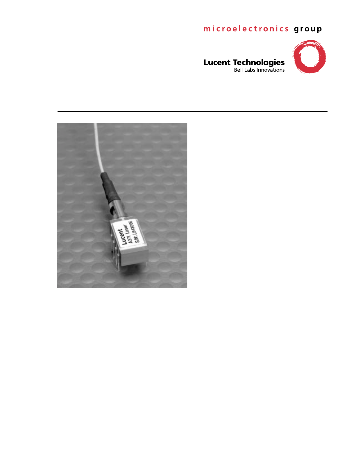
The low-profile A371-Type Analog Laser Module is ideally
suited for CATV applications, particularly in systems where
long spans and superior reliability are the critical considerations.
Features
Eight-pin package suitable for CATV applications
■
Narrow linewidth, distributed-feedback,
■
multiquantum-well (DFB-MQW)1.3 µ m laser with
single-mode fiber pigtail
Wide operating temperature range:
■
–40 ° C to +85 ° C
Frequency range up to 1.0 GHz
■
■
Qualification program: Bellcore TA-983
Applications
■
Video and data applications
■
Downstream telephony and data
■
Return path systems
■
Mixed analog and digital modulation
■
Telecommunications
Benefits
■
Easily board mounted
■
Requires no lead bending
■
No additional heat sinks required
■
Pin compatible with industry-standard, 14-pin laser
module
■
Highly efficient DFB-MQW laser structure allows
for lower threshold and drive currents , and reduced
power consumption
■
High output power allows for longer system spans ,
more fiber splits, and greater tolerance of fiber and
connector quality
■
Internal isolator minimizes spurious noise
±
°
°
A371-Type Analog Uncooled Isolated Data Sheet
DFB
FastLight
Laser Module January 1999
Description
The A371-Type Uncooled Isolated Laser Module consists of a laser diode coupled to a single-mode fiber
pigtail. The device is available in a standard, 8-pin configuration (see Figure 1 and/or Table 1) and is ideal for
CATV applications.
The module includes a narrow linewidth (<1 nm), DFBMQW, single-mode laser and an InGaAs PIN photodiode back-facet monitor in a hermetically sealed package.
The device characteristics listed in this document are
met at 2.0 mW output power. Higher- or lower-power
operation is possible. Under conditions of a fixed photodiode current, the change in optical output is typically
0.5 dB over an operating temperature range of –40 ° C
to +85 ° C.
This device incorporates the new Laser 2000 manufac-
turing process from the Optoelectronics unit of Lucent
Technologies Microelectronics Group. Laser 2000 is a
low-cost platform that targets high-volume manufacturing and tight product distributions on all optical subassemblies. This platform incorporates an advanced
optical design that is produced on Opto’s highly automated production lines. The Laser 2000 platform is
qualified for central office and uncontrolled environments, and can be used for applications requiring high
performance and low cost.
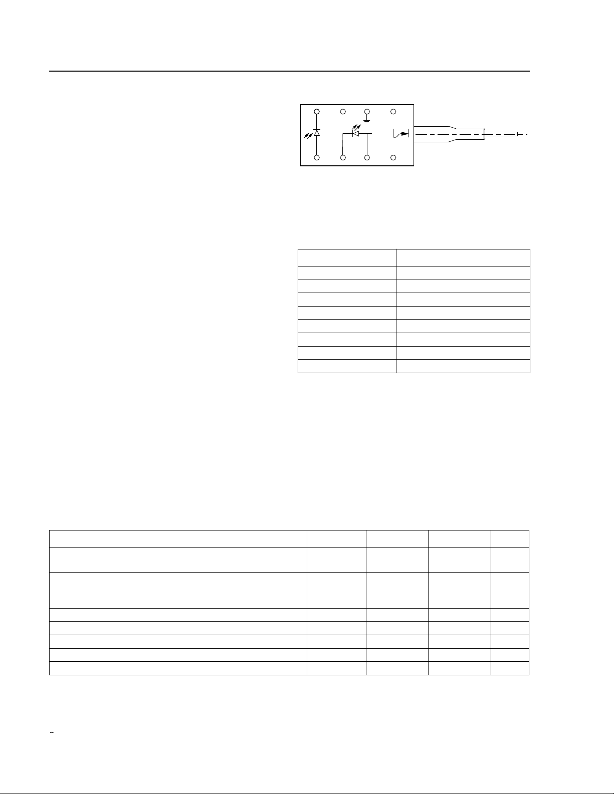
43 12
56 87
1-900 (C)
Figure 1. A371-T ype Analog Uncooled Isolated DFB
Laser Module Schematic, Top View
Table 1. Pin Descriptions
Pin Number Connection
1NC
2 Case ground
3NC
4 Photodiode cathode
5 Photodiode anode
6 Laser diode cathode
7 Laser diode anode
8NC
Absolute Maximum Ratings
Stresses in excess of the absolute maximum ratings can cause permanent damage to the device. These are absolute stress ratings only. Functional operation of the device is not implied at these or any other conditions in excess
of those given in the operations sections of the data sheet. Exposure to absolute maximum ratings for extended
periods can adversely affect device reliability.
Parameter Symbol Min Max Unit
Maximum Peak Laser Drive Current or
Maximum Fiber Power*
Peak Reverse Laser Voltage:
Laser
Monitor
Monitor Forward Current I
Operating Case Temperature Range T
Storage Case Temperature Range T
Lead Soldering Temperature/Time — — 260/10 ° C/s
Relative Humidity (noncondensing) RH — 85 %
* Rating varies with temperature.
22
OP
I
P
MAX
V
RL
RD
V
FD
C
stg
—
—
—
—
150
10
2
20
mA
mW
V
V
—2mA
–40 85
–40 85
C
C
Lucent Technologies Inc.

°
∆λ
Ω
µ
Data Sheet A371-Type Analog Uncooled Isolated
January 1999 DFB
FastLight
Laser Module
Handling Precautions
Caution: This device is susceptible to damage as a result of electrostatic discharge (ESD). Take proper
precautions during both handling and testing. Follow guidelines such as JEDEC Pub lication No.
108-A (Dec. 1988).
Although protection circuitry is designed into the device, take proper precautions to avoid exposure to ESD.
Electro/Optical Characteristics
Table 2. Electro/Optical Characteristics (over operating temperature range unless otherwise noted)
Parameter Symbol Test Conditions Min Typ Max Unit
Operating Temperature
Range
Optical Output Power* P
Threshold Current I
Drive Current Above
Threshold
Slope Efficiency SE CW, P
Center Wav elength
Spectral Width (–20 dB)
Side-mode Suppression
Ratio
Tracking Error TE I
Forward Voltage V
Input Impedance R — 3 — 8
Monitor Current I
Monitor Dark Current I
Wavelength Temperature
Coefficient
* See Table 5 for more information.
†V
R
= reverse voltage.
T — –40 — 85
F
TH
I
MOD
CW, P
CW, I
λ
C
SMSR CW, P
F
MON
D
CW, nominal — 2 — mW
T = 25 ° C
T = full range
= 2.0 mW, T = 25 ° C
F
= const., T = full range
MON
= 2.0 mW, T = 25 ° C 67 — 200 µ W/mA
F
P
= 2.0 mW, CW 1280 — 1335 nm
F
F
P
= 2.0 mW — — 1 nm
F
= 2.0 mW 30 40 — dB
MON
= constant, CW — 0.5 1.25 dB
5
2
10
7.5
11
—
20
—
15
50
30
55
CW — 1.1 1.6 V
†
V
R
= 5 V 100 — 1000
†
V
= 5 V — 10 200 nA
R
— — — 0.09 0.1 nm/ ° C
C
mA
mA
mA
A
Lucent Technologies Inc.
3
 Loading...