

AGERE 980X Datasheet
Preliminary Data Sheet
April 1999
980-Type Ultrahigh-
Reliability Pump Laser Module
The 980-Type Ultrahigh-Reli ability Pump Laser Module is ideally suited for fiber amplifier-based optical transmission systems that require a long-term life expectancy.
Features
■
Extremely high reliability
— Laser-welded packaging technology used to
attain ultrastable long-term operation
— 29-year life
■
Planar InGaAs PIN photodiode monitor for laser
back-facet output
■
Wide range of stable CW optical output power
■
Individually certified for ultrahigh reliability
■
InGaAs ridge waveguide 980 nm single-mode
laser diode
■
Standard low-profile, laser-welded, metal, hermetic, 14-pin butterfly package
■
Single-mode fiber with Bragg Grating (FBG) for
stable operation
■
Stable single spatial mode kink-free operation over
a wide range of temperatures and currents
Applications
■
Undersea optical transmission systems
■
Ultrahigh reliability optical communications for military systems
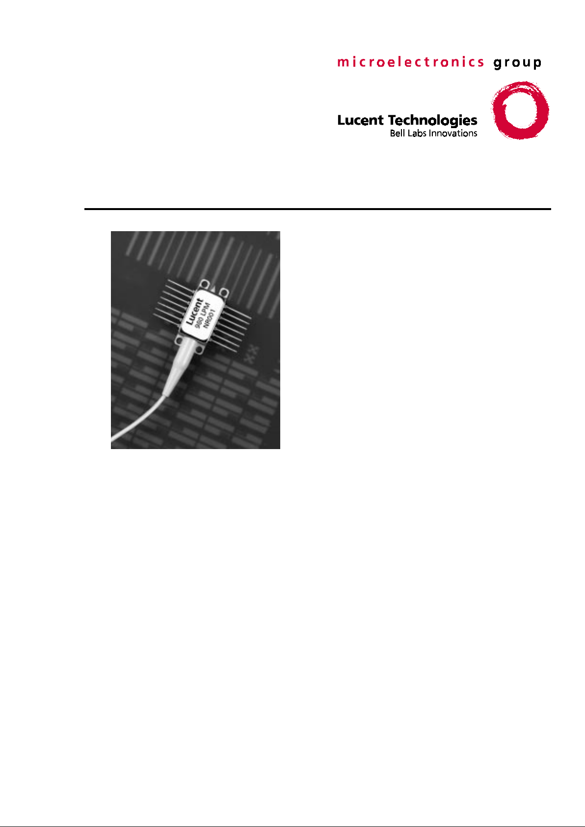
Description
The 980-Type Pump Laser Module is a precision,
high-performance, ultrahigh-reliability lightwave component that provides high output power light, in the
980 nm range. The 980-Type Pump Laser Module is
comprised of a single-mode laser diode, PIN backfacet monitor, microlensed single-mode fiber, and a
Fiber Bragg Grating (FBG) for improved stability, all
encased in a specially designed 14-pin, oxygen free,
butterfly package.
The 980-Type Pump Laser Module is capable of
providing a wide range of output power in the
974 nm to 984 nm wavelength range for erbiumdoped amplifier (EDFA) system application. The
pump laser module is designed and individually certified for high-reliability operation and long-term life
expectancy. The 980 nm InGaAs laser chip utilizes a
ridge guide design for high performance and reliability. Chip and facet parameters are optimized for stabilized optical coupling and efficient pumping of the
EDFA. The laser package design also includes a
microlensed single-mode fiber and a planar InGaAs
PIN back-facet photomonitor assembled in a modular
organic-free hermetic package. Laser welding technology is used for critical joints to achieve long-term
stability. Data is archived for at least ten years. Each
module is fully characterized and traceable. Long-life
performance and reliability are ensured through
extensive steps of burn-in, overstress, and power
aging. The 980-T ype Pump Laser Module is available
with a typical power output range of 20 mW to
70 mW.

980-Type Ultrahigh Preliminary D ata Sheet
Reliability Pump Laser Module April 1999
22
Lucent Technologies Inc.
Description
(continued)
The 980-Type Pump Laser Module has been specifically designed for undersea optical amplified very high
capacity transmission systems that require long-term
life expectancy. The extremely stringent reliability
requirements imposed on the 980-Type (necessary to
achieve long-term system life) are accomplished
through careful design, exacting manufacture, and thorough testing. The 980-Type qualification plan consists
of a basic set of electro-optic and mechanical tests
designed to confirm the performance and reliability of
the module over its projected service life under
assumed operating conditions. Custom designed,
extended qualification test programs can be developed
to focus on customer system requirements.
Based on the results of qualification testing, a certification program has been developed to ensure the highreliability performance of the devices. Each 980-Type
device undergoes this certification process where the
perf orman c e pa r a me t e rs ar e me a su re d be fore, during ,
and after environmental stresses. The certification
results for each 980-T ype Pump Laser Module are then
examined to ensure that only the pump laser modules
that exhibit performance consistent with long-term system operation are selected for product.
Each 980-Type is individually serialized for full traceability and is shipped with the appropriate test data.
The 980-Type assembly, test, and certification facilities
have all passed the rigorous qualification process
required for all facilities that manufacture devices
employed in undersea applications. Also, on an ongoing basis, small quantities of product from each manufacturing lot are retained and tested as part of a
surveillance program for undersea devices. Each surveillance group is subjected to the complete spectrum
of environmental/mechanical stresses required during
the qualification process. The surveillance results are
reviewed and compiled so that long-term trends can be
studied. The reliability performance of the 980-Type
Pump Laser Module is a result of a rigorous qualification process combined with an extensive and ongoing
surveillance program.
Pinout Information
Top View.
1-675(F).e
Figure 1. Pinout Schematic
7654321
8 9 10 11 12 13
14
Preliminary Data Sheet 980-Type Ultrahigh
April 1999 Reliability Pump Laser Module
3
Lucent Technologies Inc.
Pinout Information
(continued)
Table 1. Pinout Descriptions
Handling Precautions
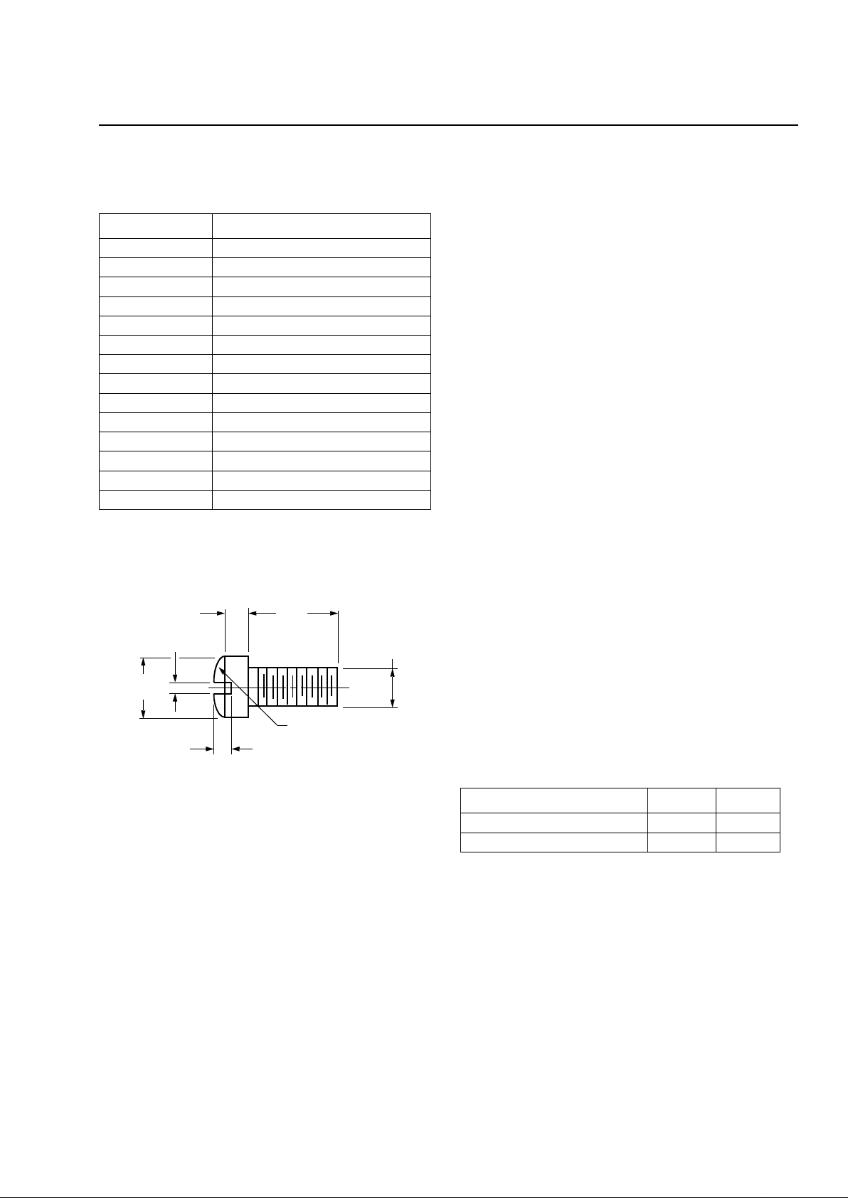
Note: Dimensions are inches and (millimeters).
1-532(F)
Figure 2. Fillister Head Screw
Power Sequencing
Adopt the following sequence for turn-on as a matter of
good practice to avoid the possibility of damage to the
pump laser module from power supply switching transients:
1. All ground connections
2. Most negative supply
3. Most positive supply
4. All remaining connections
Reverse the order for the proper turn-off sequence.
Mounting Instructions
The minimum fiber-bend radius is 25 mm.
To avoid degradation in performance, mount the mod-
ule on the board as follows (see Figure 2):
1. Place the bottom flange of the module on a flat heat
sink at least 0.5 in. x 1.180 in. (12.7 mm x 30 mm) in
size. The surface finish of the heat sink should be
better than 32 µin. (0.8 µm), and the surface flatness
must be better than 0.001 in. (25.4 µm).
Mount four #2-56 screws with Fillister heads (M23 mm) at the four screw hole locations (see Outline
Diagram). The Fillister head diameter must not exceed
0.140 in. (3.55 mm). Do not apply more than 2 in./lb. of
torque to the screws. To minimize package distortion, it
is recommended that a washer is used above and
beneath each mounting foot.
Electrostatic Discharge
Caution: This is a Class 0 ESD device which is
susceptible to damage as a result of
electrostatic discharge (ESD). Take
proper precautions during both handling
and testing. Follow JEDEC Publication
No. 108-A (Dec. 1998).
Lucent employs a human-body model (HBM) and the
field-induced charged-device model (CDM) for ESDsusceptibility testing and protection design evaluation.
ESD voltage thresholds are dependent on the critical
parameters used to define the model. A standard HBM
(resistance = 1.5 kΩ, capacitance = 100 pF) is widely
used and, therefore, can be used for comparison purposes. The HBM ESD threshhold presented here was
obtained using these circuit parameters:
Pin Connection
1 Chassis Ground
2 Chassis Ground
3 Photodetector Anode
4 Photodetector Cathode
5 Chassis Ground
6 Chassis Ground
7 Chassis Ground
8 Chassis Ground
9 Chassis Ground
10 Pump Laser Anode
11 Pump Laser Cathode
12 Chassis Ground
13 Chassis Ground
14 Chassis Ground
0.118
(3.00)
0.062 (1.58)
0.140
(3.56)
0.031 (0.79)
0.129 (3.28)
0.086
(2.18)
0.041 (1.04)
Parameter Value Unit
Charged-device Model ≥200 V
Human-body Model ≥400 V
 Loading...