

AGERE 3X38FTR Datasheet

Preliminary Data Sheet
September 2000
3X38FTR 208-Pin SQFP
OCTAL-FET (Fast Ethernet Transceiver) for 10Base-T/100Base-TX/
■
Overview
The 3X38FTR 208-Pin SQFP is an eight-channel,
single-chip complete transceiver designed specifically for dual-speed 10Base-T, 100Base-TX, and
100Base-FX switches and repeaters. It supports
simultaneous operation in three separate
IEEE
*
standard modes: 10Base-T, 100Base-TX, and
100Base-FX. The 3X38 uses 0.25 µm low-power
CMOS to achieve extremely low power dissipation
and operates from a single 3.3 V power supply.
Each channel implements the following:
■
10Base-T transceiver function of
■
100Base-TX transceiver function of
■
100Base-FX transceiver function of
■
Autonegotiation of
■
MII management of
IEEE
IEEE
802.3u.
802.3u.
IEEE
IEEE
IEEE
802.3.
802.3u.
802.3u.
The 3X38 supports operations over two pairs of
unshielded twisted-pair (UTP) cable (10Base-T and
100Base-TX) and over fiber-optic cable (100BaseFX).
It has been designed with a flexible system interface
that allows configuration for optimum performance
and effortless design. The individual per-port system
interface can be configured as 10 Mbits/s,
or
100 Mbits/s reduced MII (RMII), or 10 Mbits/s, or
100 Mbits/s serial MII (SMII).
Features
10 Mbits/s Transceiver
■
Compatible with
for category 3 unshielded twisted-pair (UTP) cable.
■
Compatible with the reduced MII (RMII) specifica-
tion of the RMII consortium version 1.2.
■
Selectable 7-pin RMII or 2-pin serial MII (SMII).
IEEE
802.3 10Base-T standard
Autopolarity detection and correction.
■
Adjustable squelch level for extended line length
capability (two levels).
■
On-chip filtering eliminates the need for external
filters.
■
Half- and full-duplex operations.
100 Mbits/s TX Transceiver
■
Compatible with
IEEE
802.3u PCS (clause 23),
PMA (clause 24), autonegotiation (clause 28), and
PMD (clause 25) specifications.
■
Compatible with the reduced MII (RMII) specifica-
tion of the RMII consortium version 1.2.
■
Selectable 7-pin RMII, 2-pin SMII (serial MII).
■
Scrambler/descrambler bypass.
■
Selectable carrier sense signal generation (CRS)
asserted during eit her tr ansm issi on o r re cepti on i n
half duplex (CRS asserted during reception only in
full duplex).
■
Full- or half-duplex operations.
■
On-chip filtering and adaptive equalization that
eliminates the need for external filters.
100 Mbits/s FX Transceiver
■
Pseudo-ECL compatible input/output for 100Base-
FX support (with fiber-optic signal detect).
■
Compatible with
dard.
■
Reuses existing twisted-pair I/O pins for compati-
ble fiber-optic transceiver pseudo-ECL (PECL)
data:
— No additional data pins required.
— Reuses existing 3X38 pins for fiber-optic
signal detect (FOSD) inputs.
IEEE
802.3u 100Base-FX stan-
FX
*
IEEE
is a registered trademark of The Institute of Electrical and Electronics Engineers, Inc.

3X38FTR 208-Pin SQFP Preliminary Data Sheet
OCTAL-FET for 10Base-T/100Base-TX/FX September 2000
■
Features
■
Fiber mode automatically configures port:
(continued)
— Disables autonegotiation.
— Disables 10Base-T.
— Enables 100Base-FX far-end fault signaling.
— Disables MLT-3 encoder/decoder.
— Disables scrambler/descrambler.
■
FX mode enable is pin- or register-selectable on an
individual per-port basis.
General
■
Low power dissipation (<0.4 W per port).
■
Autonegotiation (
— Fast link pulse (FLP) burst generator.
— Arbitration function.
■
Supports the station management protocol and
frame format (clause 22):
— Basic and extended registers.
— Supports next page mode.
— Accepts preamble suppression.
— Maskable status interrupts.
— 12.5 MHz MDC clock rate.
■
Supports the following management functions via
pins if MII station management is unavailable:
— Speed select.
— Scrambler/descrambler bypass.
— Full duplex.
— No link pulse mode.
— Carrier sense select.
— Autonegotiation.
— FX mode select.
IEEE
802.3u, cl ause 28):
Single 50 MHz/125 MHz clock input in RMII and SMII
modes, respectively.
■
Supports half- and full-duplex operations.
■
Provides four LED status signals:
— Activity (transmit or receive). Optional LED blink
mode (500 ms on, 500 ms off or 2.5 s on, 2.5 s
off) or pulse stretch mode (40 ms—80 ms).
— Full duplex or collision, automatically configured.
— Link integrity.
— Speed indication.
■
Internally generated power-on-reset configures 3X38
automatically on powerup.
■
Serial LED output stream for additional status moni-
toring.
■
Bicolor LED mode.
■
LED drivers on-chip (8 mA—10 mA). Drivers can be
turned off when LED is not used (power saving).
■
Per-channel powerdown mode for 10 Mbits/s and
100 Mbits/s operation.
■
Loopback for 10 Mbits/s and 100 Mbits/s operation.
■
Internal pull-up or pull-down resistors to set default
configuration during powerup.
■
0.25 µm low-power CMOS technology.
■
208-pin SQFP package.
■
JTAG boundary scan.
■
Single 3.3 V power supply.
2 Lucent Technologies Inc.

Preliminary Data Sheet 3X38FTR 208-Pin SQFP
September 2000 OCTAL-FET for 10Base-T/100Base-TX/FX
Table of Contents
Contents Page
Overview...................................................................................................................................................................................................1
Features....................................................................................................................................................................................................1
10 Mbits/s Transceiver........................................................................................................................................................................... 1
100 Mbits/s TX Transceiver....................................................................................................................................................................1
100 Mbits/s FX Transceiver....................................................................................................................................................................1
General .................................................................................................................................................................................................. 2
Description................................................................................................................................................................................................5
RMII Mode............................................................................................................................................................................................. 5
SMII Mode.............................................................................................................................................................................................5
LED Control...........................................................................................................................................................................................5
Clocking................................................................................................................................................................................................. 5
FX Mode................................................................................................................................................................................................ 5
Single-Channel Detail Functions...........................................................................................................................................................7
Block Diagrams......................................................................................................................................................................................8
Pin Information ....................................................................................................................................................................................... 10
Pin Diagram for RMII Mode................................................................................................................................................................. 10
Pin Diagram for SMII Mode .................................................................................................................................................................11
Pin Maps........................... ....................................................................................................................... ............................................15
Pin Descriptions......................................................................................................................................................................................16
Functional Description............................................................................................................................................................................27
Reduced Media Independent Interface (RMII)..................................................................................................................................... 27
RMII/SMII Interface.............................................................................................................................................................................. 29
Media Independent Interface (MII)—Internal ....................................................................................................................................... 31
100Base-X Module.............................. ........................................................................................................................ ........................32
100Base-TX Transceiver......................................................................................................................................................................36
10Base-T Module................................................................................................................................................................................37
Operation Modes.................................................................................................................................................................................37
LED Operational Modes......................................................................................................................................................................39
Reset Operation...................................................................................................................................................................................43
MII Station Management ........................................................................................................................................................................44
Basic Operation...................................................................................................................................................................................44
Unmanaged Operations....................................................................................................................................................................... 45
Register Information............... ................................................................................................................................................................ 46
Register Descriptions ..........................................................................................................................................................................46
Absolute Maximum Ratings................................. ...................................................................................................................................56
Clock Timing............................................................................................... .................... ........................................................................57
Outline Diagram......................................................................................................................................................................................63
208-Pin SQFP .....................................................................................................................................................................................63
Tables Page
Table 1. 3X38 Signal in Alphanumer ic Sequenc e Ac cording to Pin Number.........................................................................................1 2
Table 2. 3X38 RMII/SMII Pin Map..........................................................................................................................................................15
Table 3. RMII/SMII Interface Pins..........................................................................................................................................................16
Table 4. MII Management......................................................................................................................................................................17
Table 5. 10/100 Mbits/s Twisted-Pair (TP) Interface Pins....................................................................................................................... 18
Table 6. LED and Configuration Pins.....................................................................................................................................................18
Table 7. Table Test Mode Pins...............................................................................................................................................................24
Table 8. Clock, Reset, FOSD, and Special Configuration Pins..............................................................................................................25
Table 9. Power, Ground, and No Connects ............................................................................................................................................26
Table 10. Receive Data/Status Encoding...............................................................................................................................................30
Table 11. Symbol Code Scrambler .......................................................................................................................................................33
Table 12. LED Modes ............................................................................................................................................................................40
Table 13. Serial LED Pin Descriptions...................................................................................................................................................41
Table 14. Serial LED Port Order............................................................................................................................................................41
Table 15. Bicolor Mode..........................................................................................................................................................................4 2
Table 16. Bicolor LED Mode Descriptions .............................................................................................................................................43
Table 17. MII Management Frame Format.................... ................................................................................ ......................................... 44
Table 18. MII Management Frames—Field Descriptions................. .................................................................................................... ..44
Lucent Technologies Inc. 3

3X38FTR 208-Pin SQFP Preliminary Data Sheet
OCTAL-FET for 10Base-T/100Base-TX/FX September 2000
Table of Contents
Tables
Table 19. PHY Addresses ......................................................................................................................................................................45
Table 20. Output Pins.............................................................................................................................................................................45
Table 21. Summary of Management Registers (MR).............................................................................................................................46
Table 22. MR0—Control Register Bit Descriptions.................................................................................................................................46
Table 23. MR1—Status Register Bit Descriptions..................................................................................................................................47
Table 24. MR2, MR3—PHY Identification Registers (1 and 2) Bit Descriptions.....................................................................................48
Table 25. MR4—Autonegotiation Advertisement Register Bit Descriptions...........................................................................................48
Table 26. MR5—Autonegotiation Link Partner Ability (Base Page) Register Bit Descriptions................................................................49
Table 27. MR5—Autonegotiation Link Partner (LP) Ability Register (Next Page) Bit Descriptions.........................................................49
Table 28. MR6—Autonegotiation Expansion Register Bit Descriptions..................................................................................................50
Table 29. MR7—Next Page Transmit Register Bit Descriptions .............................................................................................................50
Table 30. MR20—LED and FIFO Configuration.....................................................................................................................................51
Table 31. MR21—RXER Counter...........................................................................................................................................................51
Table 32. MR28—Device-Specific Register 1 (Status Register) Bit Descriptions...................................................................................52
Table 33. MR29—Device-Specific Register 2 (100 Mbits/s Control) Bit Descriptions............................................................................53
Table 34. MR30—Device-Specific Register 3 (10 Mbits/s Control) Bit Descriptions........................... ...................................................54
Table 35. MR31—Device-Specific Register 4 (Quick Status) Bit Descriptions.......................................................................................55
Table 36. Absolute Maximum Ratings....................................................................................................................................................56
Table 37. Operating Conditions..............................................................................................................................................................56
Table 38. dc Characteristics...................................................................................................................................................................56
Table 39. System Clock (RMII Mode).....................................................................................................................................................57
Table 40. Management Clock .................................................................................................................................................................57
Table 41. RMII Receive Timing...............................................................................................................................................................58
Table 42. RMII Transmit Timing..............................................................................................................................................................58
Table 43. Transmit Timing.......................................................................................................................................................................59
Table 44. SMII Timing.............................................................................................................................................................................59
Table 45. Receive Timing.......................................................................................................................................................................60
Table 46. Reset and Configuration Timing.............................................................................................................................................61
Table 47. PMD Characteristics...............................................................................................................................................................62
(continued)
Page
(continued)
Figures Page
Figure 1. 3X38 Device Overview..............................................................................................................................................................6
Figure 2. 3X38 Single-Channel Detail Functions.....................................................................................................................................7
Figure 3. Typical Single-Channel Twisted-Pair (TP) Interface ..................................................................................................................8
Figure 4. Typical Single-Channel Fiber-Optic (FX) Interface....................................................................................................................9
Figure 5. 3X38 Pinout for RMII Mode.....................................................................................................................................................10
Figure 6. 3X38 Pinout for SMII Mode.....................................................................................................................................................11
Figure 7. Functional Description............................................................................................................................................................27
Figure 8. RMII Receive Timing from Internal MII Signals.......................................................................................................................28
Figure 9. SMII Connection Diagram.......................................................................................................................................................29
Figure 10. Receive Sequence Diagram .................................................................................................................................................29
Figure 11. Transmit Sequence Diagram.................................................................................................................................................30
Figure 12. 100Base-X Data Path ...........................................................................................................................................................32
Figure 13. 10Base-T Module Data Path.................................................................................................................................................37
Figure 14. Timing Diagram .....................................................................................................................................................................42
Figure 15. Hardware Reset Configuration..............................................................................................................................................43
Figure 16. System Clock........................................................................................................................................................................57
Figure 17. Management Clock...............................................................................................................................................................57
Figure 18. RMII Receive Timing.............................................................................................................................................................58
Figure 19. RMII Transmit Timing............................................................................................................................................................58
Figure 20. Transmit Timing .....................................................................................................................................................................59
Figure 21. SMII Timing...........................................................................................................................................................................59
Figure 22. Receive Timing .....................................................................................................................................................................60
Figure 23. Reset and Configuration Timing............................................................................................................................................61
Figure 24. PMD Characteristics .............................................................................................................................................................62
4 Lucent Technologies Inc.

Preliminary Data Sheet 3X38FTR 208-Pin SQFP
September 2000 OCTAL-FET for 10Base-T/100Base-TX/FX
Description
RMII Mode
The reduced media independent interface (RMII) is a
low pin count interface specification promulgated by the
RMII consortium. This specification reduces the total
number of pins from 16 for the
face to seven for the RMII. Architecturally, the RMII
specification provides for an additional reconciliation
sublayer on either side of the MII but, in the 3X38, has
been implemented in the absence of the MII.
The management interface (MDIO/MDC) remains identical to that defined in
IEEE
The RMII specification has the following characteristics:
■
It supports 10 Mbits/s and 100 Mbits/s data rates.
■
A single 50 MHz clock reference is sourced from
MAC to PHY or from an external shared source.
■
It provides independent 2-bit wide transmit and
receive data paths.
IEEE
802.3u.
802.3U MII inter-
LED Control
LEDs can be accessed in one of the following modes:
■
Serial mode. In this mode, all of the LEDs are timedivision multiplexed onto one pin, with a second pin
acting as the clock and a third as a strobe. All LEDs
and all channels share the same pins.
■
Parallel mode. In this mode, each LED and each
channel has its own pin. There is a total of four LED
pins per channel for a total of 32 pins.
■
Bicolor mode. In this mode, each channel has two
outputs to control a bicolor LED. One LED can be
used for each port, indicating link and activity.
In all modes, the LEDs can be operated as
follows:
■
LED stretch.
■
LED blink.
■
No stretch or blink.
Clocking
SMII Mode
The serial media independent interface (SMII) is a low
pin count interface specification promulgated by
Cisco
*. This specification reduces the total number of
pins from 16 for the
the SMII. Architecturally, the SMII specification provides for an additional reconciliation sublayer on either
side of the MII but, in the 3X38, has been implemented
in the absence of the MII.
The management interface (MDIO/MDC) remains identical to that defined in
The SMII specification has the following characteristics:
■
It supports 10 Mbits/s and 100 Mbits/s data rates.
■
A single 125 MHz clock reference is sourced from
MAC to PHY or from an external shared source.
■
It provides independent serial transmit and receive
data paths.
IEEE
802.3u MII interface to two for
IEEE
802.3u.
The 3X38 operates with a 50 MHz clock input when in
the RMII mode, and with a 125 MHz clock input when
in the SMII mode.
FX Mode
Each individual port of the 3X38 can be operated in
100Base-FX mode by selecting it through the pin program option (FX_MODE_EN[7:0]), or through the register bit (register 29, bit 0).
When operating in FX mode, the twisted-pair I/O pins
are reused as the fiber-optic transceiver I/O data pins,
and the fiber-optic signal detect (FOSD) inputs are
enabled.
When a port is placed in FX mode, it will automatically
configure the port for 100Base-FX operation (and the
register bit control will be ignored) such that:
■
The far-end fault signaling option will be enabled.
■
The MLT-3 encoding/decoding will be disabled.
■
Scrambler/descrambler will be disabled.
■
Autonegotiation will be disabled.
■
The signal detect inputs will be activated.
■
10Base-T will be disabled.
*
Cisco
is a registered trademark of Cisco Systems.
Lucent Technologies Inc. 5
3X38FTR 208-Pin SQFP Preliminary Data Sheet
OCTAL-FET for 10Base-T/100Base-TX/FX September 2000
Description
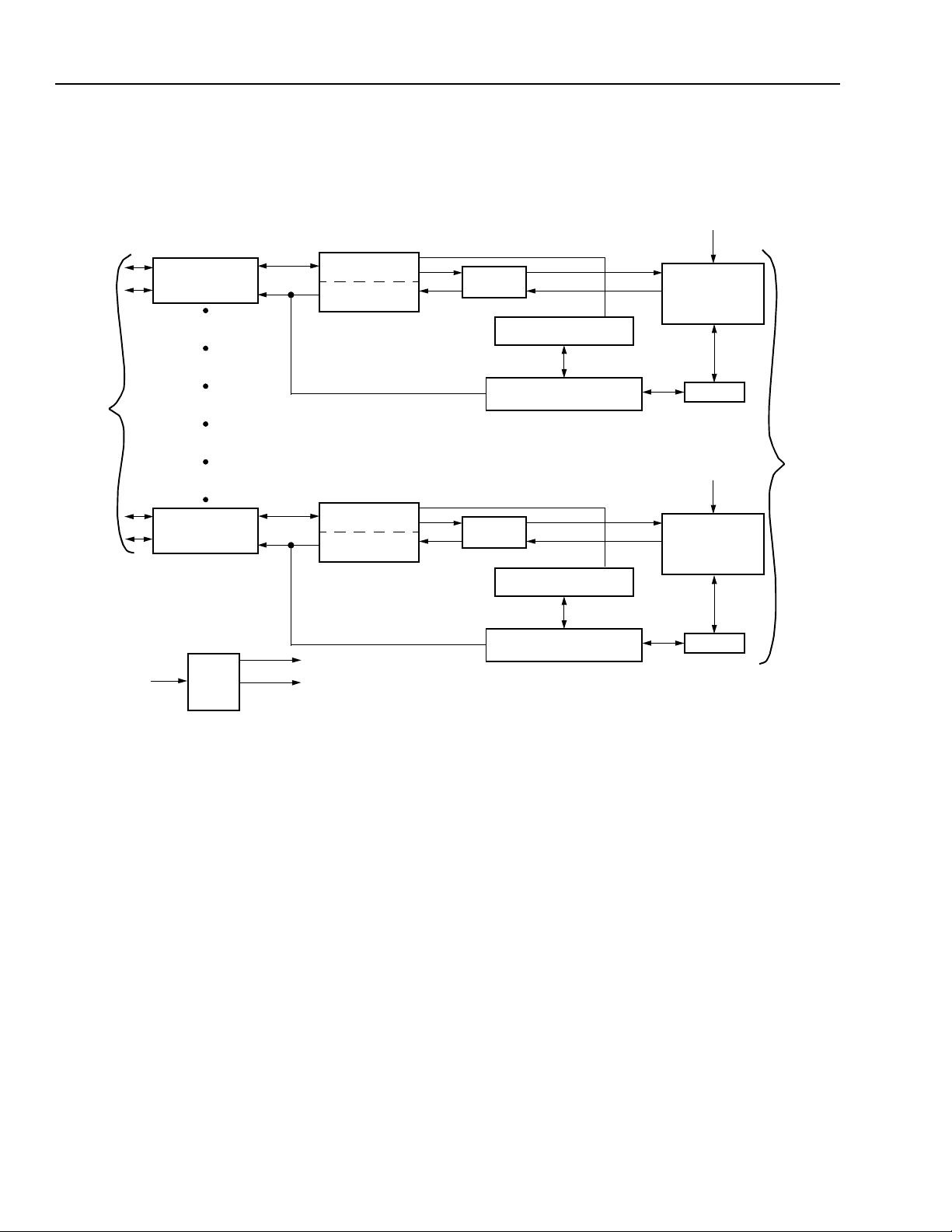
Device Overview
RMII/SMII
INTERFAC E
(continued)
PORT 0
RMII/SMII
INTERFAC E
PORT [1—6]
RMII/SMII
INTERFACE
PORT 7
MANAGEMENT
PCS
MANAGEMENT
PCS
PMA
AUTONEGOTIATION
10 Mbits/s TRANSCEIVER
DRIVER AND FILTERS
PMA
AUTONEGOTIATION
FX_MODE_EN
TX PMD/
FX PORT
DRIVER AND
FILTERS
MUX
FX_MODE_EN
TX PMD/
FX PORT
DRIVER AND
FILTERS
INTERFACE
TP MAGNETICS
50 MHz/125 MHz
RMCLK
PLL
25 MHz
125 MHz
10 Mbits/s TRANSCEIVER
DRIVER AND FILTERS
Figure 1. 3X38 Device Overview
MUX
5-6878(F).c
6 Lucent Technologies Inc.
Preliminary Data Sheet 3X38FTR 208-Pin SQFP
September 2000 OCTAL-FET for 10Base-T/100Base-TX/FX
Description
(continued)
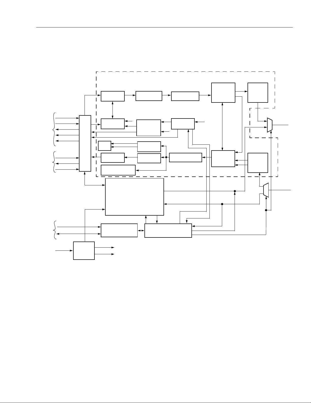
Single-Channel Detail Functions
100 Mbits/s TRANSCEIVER
SMII RMII
TXD[1:0]
TX_EN
CRS_DV
RXD[1:0]
RX_ER
TXD
RXD
SYNC
INTERFACE
MTXD[3:0]
RMII/
SMII
TO
MII
RMII/SMII
4B/5B
ENCODER
TX STATE
MACHINE
CAR_STAT
CIM
RXERR_ST
5B/4B
DECODER
FAR-END
FAULT DETECT
10 Mbits/s TRANSCEIVER
FAULT GEN.
SD
COLLISION
FAR-END
DETECT
CARRIER
DETECT
ALIGNER
SCRAMBLER
RX STATE
MACHINE
SD
DESCRAMBLER
SD
PDT
PDR/
DCRU
SD
PMD
TX
PMD
RX
TPOUT
±
TPIN
±
MANAGEMENT
50 MH
INTERFACE
RMCLK
Z
/125 MH
MDC
MDIO
Z
20 MHz
FREQ.
SYNTH.
LC100
LS100
MANAGEMENT
25 MHz
125 MHz
MII
LC10 LS10
AUTONEGOTIATION
AND LINK MONITOR
Figure 2. 3X38 Single-Channel Detail Functions
5-5136(F).kr2
Lucent Technologies Inc. 7
3X38FTR 208-Pin SQFP Preliminary Data Sheet
OCTAL-FET for 10Base-T/100Base-TX/FX September 2000
Description
(continued)
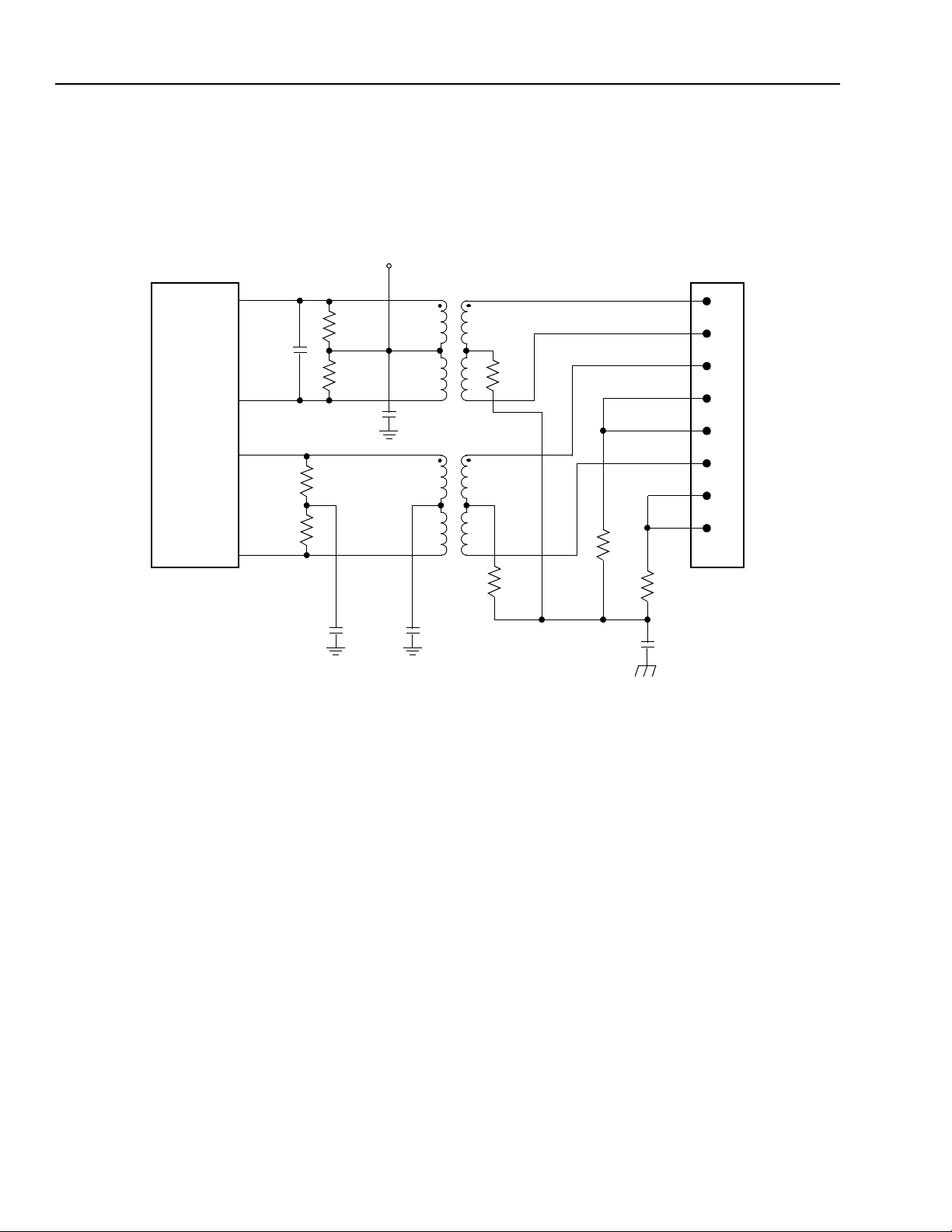
Block Diagrams
Single-Channel Twisted-Pair Interface
TPOUT+
6 pF
TPOUT–
3X38
TPIN+
Ω
50
Ω
50
TPIN–
51.1
51.1
DDO
V
1:1
Ω
Ω
0.01 µF
1:1
75
75
Ω
Ω
75
Ω
75
RJ-45
1
2
3
4
5
6
7
8
Ω
0.01 µF
0.01 µF
Figure 3. Typical Single-Channel Twisted-Pair (TP) Interface
1000 pF 2 kV
5-5433(F).sr1
8 Lucent Technologies Inc.
Preliminary Data Sheet 3X38FTR 208-Pin SQFP
September 2000 OCTAL-FET for 10Base-T/100Base-TX/FX
Description
(continued)
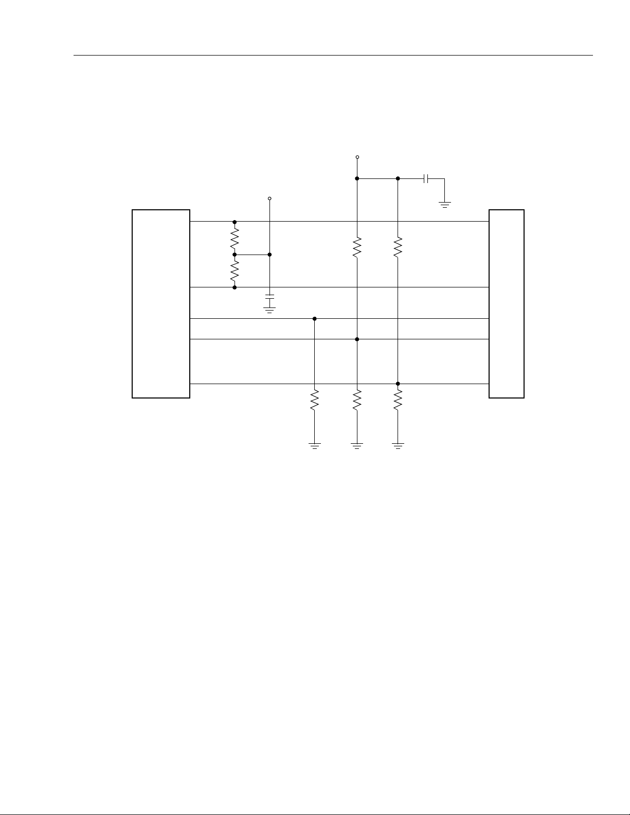
Single-Channel Fiber-Optic Interface
TPOUT+
Ω
40
Ω
40
TPOUT–
3X38
FOSD
TPIN+
TPIN–
0.01 µF
V
DDO
200
DD
V
0.01 µF
TD
Ω
127
∗
Ω
82.5
∗
Ω
127
82.5
Ω
TDN
SD
RD
RDN
∗
Ω
3.3 V FIBER
TRANSCEIVER
* These terminations per fiber modules recommendation (as shown for
Siemens
†
is a registered trademark of Siemens Aktiegesellschaft.
Figure 4. Typical Single-Channel Fiber-Optic (FX) Interface
Siemens
†
V23809-C8-C10).
5-5433(F).qr1
Lucent Technologies Inc. 9

3X38FTR 208-Pin SQFP Preliminary Data Sheet
OCTAL-FET for 10Base-T/100Base-TX/FX September 2000
Pin Information
Pin Diagram for RMII Mode
ACTLED_5/BIACTLED_5/CARIN_EN
ACTLED_3/BIACTLED_3/SCRAM_DESC_BYPASS
ACTLED_4/BIACTLED_4/AUTO_EN
ACTLED_2/BIACTLED_2/LITF_EN
ACTLED_1 /BIA CT LE D_ 1/B LIN K _ LE D_ M O D E
ACTLED_0/BIACTLED_0/STRETCH_LED
RRXD0_7
RRXD1_7
RCRS_DV_7
RRXER_7
RTXD1_7
RTXEN_7
RCRS_DV_6
RRXER_6
RRXD1_6
RRXD0_6
RTXD0_7
RTXD1_6
RTXEN_6
RTXD0_6
RRXD1_5
RCRS_DV_5
RRXER_5
RRXD0_5
RTXD1_5
RTXD0_5
RCRS_DV_4
RTXEN_5
RRXD1_4
RTXD0_4
RRXER_4
RRXD0_4
RTXD1_4
RCRS_DV_3
RTXEN_4
RRXD1_3
RRXD0_3
RTXD0_3
RTXD1_3
RRXER_3
RCRS_DV_2
RTXEN_3
RRXD1_2
RTXD0_2
RRXER_2
RRXD0_2
RTXD1_2
RTXEN_2
ACTLED_6/BIACTLED_6
ACTLED_7/BIACTLED_7
SPEEDLED_0/PHY_ADD[0]
SPEEDLED_1/PHY_ADD[1]
SPEEDLED_2/PHY_ADD[2]
SPEEDLED_3/NO_LP
VDDSPEEDLED_4/LED_MODE0
SPEEDLED_5/LED_MODE1
SPEEDLED_6
SPEEDLED_7
FDUPLED_0/SERCLK/CRS_SEL
208
207
206
205
204
203
202
201
200
199
198
1 156
V
SS
2
3
4
5
6
7
8
9
10
11
12
13
14
15
V
DD
16
17
18
19
20
21
22
23
24
25
26
27
28
29
30
V
DD
31
32
33
34
35
36
37
38
39
40
41
42
43
44
45
V
DD
46
47
48
49
50
51
RMII MODE
52
54555657585960616263646566676869707172737475767778798081828384858687888990919293949596979899100
53
197
FDUPLED_1/SERDATA/FULL_DUP
FDUPLED_2/SE RS TRO B E/ISOL ATE
196
195
VSSVDDVSSV
194
193
192
DDAVDDA
191
DDA
PECP
PECN
ATBON
ATBOP
V
FOSD0
FOSD1
190
189
188
187
186
185
184
183
3X38FTR 208-PIN SQFP
FOSD2
FOSD3
FOSD4
FOSD5
FOSD6
FOSD7
FDUPLED_3/RESERVED
FDUPLED_4/RMII_MODE
VDDFDUPLED_5/SPEED
FDUPLED_6
FDUPLED_7
LINKLED_0/BLINKLED0/FX_MODE_EN0
LINKLED_1/BLINKLED1/FX_MODE_EN1
LINKLED_2/BLINKLED2/FX_MODE_EN2
VDDLINKLED_3/BLINKLED3/FX_MODE_EN3
182
181
180
179
178
177
176
175
174
173
172
171
170
169
168
167
166
LINKLED_4/BLINKLED4/FX_MODE_EN4
165
LINKLED_5/BLINKLED5/FX_MODE_EN5
164
LINKLED_6/BLINKLED6/FX_MODE_EN6
163
LINKLED_7/BLINKLED7/FX_MODE_EN7
162
TDI
VSSVSSVSSV
161
160
101
159
102
158
103
SS
157
155
154
153
152
151
150
149
148
147
146
145
144
143
142
141
140
139
138
137
136
135
134
133
132
131
130
129
128
127
126
125
124
123
122
121
120
119
118
117
116
115
114
113
112
111
110
109
108
107
106
105
104
V
DDA
TPIN+7/FO IN +7
TPIN–7/FO IN–7
V
DDA
TPIN+6/FO IN +6
TPIN–6/FO IN–6
V
DDA
TPIN+5/FO IN +5
TPIN–5/FO IN–5
V
DDA
TPIN+4/FO IN +4
TPIN–4/FO IN–4
V
SS
V
DDA
TPIN+3/FO IN +3
TPIN–3/FO IN–3
V
DDA
TPIN+2/FO IN +2
TPIN–2/FO IN–2
V
DDA
TPIN+1/FO IN +1
TPIN–1/FO IN–1
V
SS
V
DDA
TPIN+0/FO IN +0
TPIN–0/FO IN–0
V
SS
REXTBS
V
DDA
V
DDPLL
RMCLK
V
SS
V
DDA
REXT100
REXT10
V
SS
TPOUT–7/FOOUT–7
TPOUT+7/FOOUT+7
TPOUT–6/FOOUT–6
TPOUT+6/FOOUT+6
TPOUT–5/FOOUT–5
TPOUT+5/FOOUT+5
TPOUT–4/FOOUT–4
TPOUT+4/FOOUT+4
TPOUT–3/FOOUT–3
TPOUT+3/FOOUT+3
TPOUT–2/FOOUT–2
TPOUT+2/FOOUT+2
TPOUT–1/FOOUT–1
TPOUT+1/FOOUT+1
TPOUT–0/FOOUT–0
TPOUT+0/FOOUT+0
SS
DD
V
V
RTXD1_1
RRXD1_1
RTXD0_1
RRXD0_1
RTXEN_1
RRXD1_0
RRXER_1
RCRS_DV_1
RRXD0_0
RRXER_0
RCRS_DV_0
DD
V
O_M
RTXD1_0
RTXEN_0
MDC
MDIO
3-STATE
RTXD0_0
IDDQ
TMODE4
TMODE3
TMODE2
TMODE1
TMODE0
RESET_NOT
SSVSS
SS
SS
SS
SS
SS
SS
DD
V
TCLK
NC
NC
NCNCNC
V
V
TMS
TDO
TRST
NC
V
V
V
SS
NC
NC
NC
V
V
V
MASK_STAT_INT
5-8123(F)
Figure 5. 3X38 Pinout for RMII Mode
10 Lucent Technologies Inc.
Preliminary Data Sheet 3X38FTR 208-Pin SQFP
September 2000 OCTAL-FET for 10Base-T/100Base-TX/FX
Pin Information
(continued)
Pin Diagram for SMII Mode
V
STXD_7
STXD_6
SRXD_7
SRXD_6
STXD_5
SSYNC_7:4
SRXD_5
STXD_4
SRXD_4
STXD_3
SRXD_3
STXD_2
SRXD_2
SSYNC_3:0
SS
NC
NC
NC
NC
NC
V
DD
NC
NC
NC
NC
NC
NC
NC
NC
V
DD
NC
NC
NC
NC
NC
NC
NC
NC
NC
NC
V
DD
NC
NC
NC
NC
NC
ACTLED_5/BIACTLED_5/CARIN_EN
ACTLED_3/BIACTLED_3/ SCR AM _ DES C _B YP AS S
ACTLED_4/BIACTLED_ 4/AU TO_E N
ACTLED_2/BIACTLED_2/LITF_EN
ACTLED_1/BIACTLED_1/B LINK_LE D _M ODE
ACTLED_0/BIACTLED_0/STRETCH_LED
ACTLED_6/BIACTLED_ 6
ACTLED_7/BIACTLED_ 7
SPEEDLED_0/PHY_A D D[0]
SPEEDLED_1/PHY_A D D[1]
SPEEDLED_2/PHY_A D D[2]
SPEEDLED_3/NO_LP
VDDSPEEDLED_4/LED_MODE0
SPEEDLED_5/LED_MODE1
SPEEDLED_6
SPEEDLED_7
FDUPLED_0/SERCLK/CRS_SEL
208
207
206
205
204
203
202
201
200
199
198
1 156
2
3
4
5
6
7
8
9
10
11
12
13
14
15
16
17
18
19
20
21
22
23
24
25
26
27
28
29
30
31
32
33
34
35
36
37
38
39
40
41
42
43
44
45
46
47
48
49
50
51
SMII MODE
52
54555657585960616263646566676869707172737475767778798081828384858687888990919293949596979899100
53
197
DDAVDDA
FDUPLED_1/SERDATA/FULL_DUP
FDUPLED_2/SERSTROBE/ISOLATE
VSSVDDVSSV
196
195
194
193
192
191
DDA
PECP
PECN
ATBON
ATBOP
V
FOSD0
FOSD1
190
189
188
187
186
185
184
183
3X38FTR 208-PIN SQFP
FOSD2
FOSD3
FOSD4
FOSD5
FOSD6
FOSD7
FDUPLED_3/RESERVED
FDUPLED_4/RMII_MODE
VDDFDUPLED_5/SPEED
FDUPLED_6
FDUPLED_7
LINKLED_0/BLINKLED0/FX _M ODE _E N 0
LINKLED_1/BLINKLED1/FX _M ODE _E N 1
LINKLED_2/BLINKLED2/FX _M ODE _E N 2
VDDLINKLED_3/BLINKLED3/FX _M ODE _E N 3
LINKLED_4/BLINKLED4/FX _M ODE _E N 4
LINKLED_5/BLINKLED5/FX _M ODE _E N 5
LINKLED_6/BLINKLED6/FX _M ODE _E N 6
LINKLED_7/BLINKLED7/FX _M ODE _E N 7
TDI
VSSVSSVSSV
182
181
180
179
178
177
176
175
174
173
172
171
170
169
168
167
166
165
164
163
162
161
160
159
158
101
102
103
SS
157
155
154
153
152
151
150
149
148
147
146
145
144
143
142
141
140
139
138
137
136
135
134
133
132
131
130
129
128
127
126
125
124
123
122
121
120
119
118
117
116
115
114
113
112
111
110
109
108
107
106
105
104
V
DDA
TPIN+7/FO IN+7
TPIN–7/FOIN–7
V
DDA
TPIN+6/FO IN+6
TPIN–6/FOIN–6
V
DDA
TPIN+5/FO IN+5
TPIN–5/FOIN–5
V
DDA
TPIN+4/FO IN+4
TPIN–4/FOIN–4
V
SS
V
DDA
TPIN+3/FO IN+3
TPIN–3/FOIN–3
V
DDA
TPIN+2/FO IN+2
TPIN–2/FOIN–2
V
DDA
TPIN+1/FO IN+1
TPIN–1/FOIN–1
V
SS
V
DDA
TPIN+0/FO IN+0
TPIN–0/FOIN–0
V
SS
REXTBS
V
DDA
V
DDPLL
RMCLK
V
SS
V
DDA
REXT100
REXT10
V
SS
TPOUT–7/FOOUT–7
TPOUT+7/FOOUT+7
TPOUT–6/FOOUT–6
TPOUT+6/FOOUT+6
TPOUT–5/FOOUT–5
TPOUT+5/FOOUT+5
TPOUT–4/FOOUT–4
TPOUT+4/FOOUT+4
TPOUT–3/FOOUT–3
TPOUT+3/FOOUT+3
TPOUT–2/FOOUT–2
TPOUT+2/FOOUT+2
TPOUT–1/FOOUT–1
TPOUT+1/FOOUT+1
TPOUT–0/FOOUT–0
TPOUT+0/FOOUT+0
NCNCNC
DD
NC
NC
NC
NC
V
V
STXD_0
SRXD_1
NC
STXD_1
DD
NC
NC
V
O_M
MDC
MDIO
SRXD_0
3-STATE
IDDQ
TMODE4
TMODE3
TMODE2
TMODE1
TMODE0
SS
SSVSS
SS
SS
SS
SS
SS
SS
DD
V
TCLK
NC
NC
NCNCNC
V
V
TMS
TDO
TRST
NC
V
V
V
SS
NC
NC
NC
V
V
V
RESET_NOT
MASK_STAT_INT
5-8124(F).r1
Figure 6. 3X38 Pinout for SMII Mode
Lucent Technologies Inc. 11

3X38FTR 208-Pin SQFP Preliminary Data Sheet
OCTAL-FET for 10Base-T/100Base-TX/FX September 2000
Pin Information
(continued)
Table 1. 3X38 Signal in Alphanumeric Sequence According to Pin Number
Name RMII Mode Name SMII Mode Name
1V
SS
V
SS
2 ACTLED_5 ACTLED_5
3 ACTLED_4 ACTLED_4
4 ACTLED_3 ACTLED_3
5 ACTLED_2 ACTLED_2
6 ACTLED_1 ACTLED_1
7 ACTLED_0 ACTLED_0
8 RRXD0_7 NC
9 RRXD1_7 NC
10 RCRS_DV_7 STXD_7
11 RRXER_7 NC
12 RTXD1_7 NC
13 RTXEN_7 NC
14 RCRS_DV_6 STXD_6
15 V
DD
V
DD
16 RRXER_6 NC
17 RRXD1_6 NC
18 RRXD0_6 NC
19 RTXD0_7 SRXD_7
20 RTXD1_6 NC
21 RTXEN_6 NC
22 RTXD0_6 SRXD_6
23 RRXD1_5 NC
24 RCRS_DV_5 STXD_5
25 RRXER_5 SSYNC_7:4
26 RRXD0_5 NC
27 RTXD1_5 NC
28 RTXD0_5 SRXD_5
29 RCRS_DV_4 STXD_4
30 V
DD
V
DD
31 RTXEN_5 NC
32 RRXD1_4 NC
33 RTXD0_4 SRXD_4
34 RRXER_4 NC
35 RRXD0_4 NC
36 RTXD1_4 NC
37 RCRS_DV_3 STXD_3
38 RTXEN_4 NC
39 RRXD1_3 NC
40 RRXD0_3 NC
41 RTXD0_3 SRXD_3
42 RTXD1_3 NC
43 RRXER_3 NC
Name RMII Mode Name SMII Mode Name
44 RCRS_DV_2 STXD_2
45 V
46 RTXEN_3 NC
47 RRXD1_2 NC
48 RTXD0_2 SRXD_2
49 RRXER_2 SSYNC_3:0
50 RRXD0_2 NC
51 RTXD1_2 NC
52 RTXEN_2 NC
53 RRXD1_1 NC
54 RCRS_DV_1 STXD_1
55 RRXD0_1 NC
56 RRXER_1 NC
57 RTXD1_1 NC
58 RTXEN_1 NC
59 RTXD0_1 SRXD_1
60 V
61 RRXD1_0 NC
62 RCRS_DV_0 STXD_0
63 RRXD0_0 NC
64 RRXER_0 NC
65 V
66 RTXD1_0 NC
67 O_M O_M
68 RTXEN_0 NC
69 MASK_STAT_INT MASK_STAT_INT
70 RTXD0_0 SRXD_0
71 V
72 RESET_NOT RESET_NOT
73 3-STATE 3-STATE
74 MDC MDC
75 MDIO MDIO
76 TMODE4 TMODE4
77 TMODE3 TMODE3
78 TMODE2 TMODE2
79 TMODE1 TMODE1
80 TMODE0 TMODE0
81 IDDQ IDDQ
82 V
83 TCLK TCLK
84 TRST TRST
85 TMS TMS
86 TDO TDO
DD
DD
SS
DD
DD
V
DD
V
DD
V
SS
V
DD
V
DD
12 Lucent Technologies Inc.

Preliminary Data Sheet 3X38FTR 208-Pin SQFP
September 2000 OCTAL-FET for 10Base-T/100Base-TX/FX
Pin Information
(continued)
Table 1. 3X38 Signal in Alphanumeric Sequence According to Pin Number
Name RMII Mode Name SMII Mode Name
87 V
88 V
SS
SS
V
SS
V
SS
89 NC NC
90 V
SS
V
SS
91 NC NC
92 V
SS
V
SS
93 NC NC
94 NC NC
95 NC NC
96 V
SS
V
SS
97 NC NC
98 V
SS
V
SS
99 NC NC
100 V
SS
V
SS
101 NC NC
102 V
SS
V
SS
103 NC NC
104 V
SS
V
SS
105 TPOUT+0 TPOUT+0
106 TPOUT–0 TPOUT–0
107 TPOUT+1 TPOUT+1
108 TPOUT–1 TPOUT–1
109 TPOUT+2 TPOUT+2
110 TPOUT–2 TPOUT–2
111 TPOUT+3 TPOUT+3
112 TPOUT–3 TPOUT–3
113 TPOUT+4 TPOUT+4
114 TPOUT–4 TPOUT–4
115 TPOUT+5 TPOUT+5
116 TPOUT–5 TPOUT–5
117 TPOUT+6 TPOUT+6
118 TPOUT–6 TPOUT–6
119 TPOUT+7 TPOUT+7
120 TPOUT–7 TPOUT–7
121 V
SS
V
SS
122 REXT10 REXT10
123 REXT100 REXT100
124 V
125 V
DDA
SS
V
V
DDA
SS
126 RMCLK RMCLK
127 V
128 V
DDPLL
DDA
V
DDPLL
V
DDA
129 REXTBS REXTBS
Name RMII Mode Name SMII Mode Name
130 V
131 TPIN–0 TPIN–0
132 TPIN+0 TPIN+0
133 V
134 V
135 TPIN–1 TPIN–1
136 TPIN+1 TPIN+1
137 V
138 TPIN–2 TPIN–2
139 TPIN+2 TPIN+2
140 V
141 TPIN–3 TPIN–3
142 TPIN+3 TPIN+3
143 V
144 V
145 TPIN–4 TPIN–4
146 TPIN+4 TPIN+4
147 V
148 TPIN–5 TPIN–5
149 TPIN+5 TPIN+5
150 V
151 TPIN–6 TPIN–6
152 TPIN+6 TPIN+6
153 V
154 TPIN–7 TPIN–7
155 TPIN+7 TPIN+7
156 V
157 V
158 V
159 V
160 V
161 TDI TDI
162 LINKLED_7 LINKLED_7
163 LINKLED_6 LINKLED_6
164 LINKLED_5 LINKLED_5
165 LINKLED_4 LINKLED_4
166 LINKLED_3 LINKLED_3
167 V
168 LINKLED_2 LINKLED_2
169 LINKLED_1 LINKLED_1
170 LINKLED_0 LINKLED_0
171 FDUPLED_7 FDUPLED_7
172 FDUPLED_6 FDUPLED_6
(continued)
SS
DDA
SS
DDA
DDA
DDA
SS
DDA
DDA
DDA
DDA
SS
SS
SS
SS
DD
V
V
V
V
V
V
V
V
V
V
V
V
V
V
V
V
SS
DDA
SS
DDA
DDA
DDA
SS
DDA
DDA
DDA
DDA
SS
SS
SS
SS
DD
Lucent Technologies Inc. 13

3X38FTR 208-Pin SQFP Preliminary Data Sheet
OCTAL-FET for 10Base-T/100Base-TX/FX September 2000
Pin Information
(continued)
Table 1. 3X38 Signal in Alphanumeric Sequence According to Pin Number
Name RMII Mode Name SMII Mode Name
173 FDUPLED_5 FDUPLED_5
174 V
DD
V
DD
175 FDUPLED_4 FDUPLED_4
176 FDUPLED_3 FDUPLED_3
177 FOSD7 FOSD7
178 FOSD6 FOSD6
179 FOSD5 FOSD5
180 FOSD4 FOSD4
181 FOSD3 FOSD3
182 FOSD2 FOSD2
183 FOSD1 FOSD1
184 FOSD0 FOSD0
185 V
DDA
V
DDA
186 ATBOP ATBO P
187 ATBON ATBON
188 PECN PECN
189 PECP PECP
190 V
DDA
V
DDA
Name RMII Mode Name SMII Mode Name
191 V
192 V
193 V
194 V
195 FDUPLED_2 FDUPLED_2
196 FDUPLED_1 FDUPLED_1
197 FDUPLED_0 FDUPLED_0
198 SPEEDLED_7 SPEEDLED_7
199 SPEEDLED_6 SPEEDLED_6
200 SPEEDLED_5 SPEEDLED_5
201 SPEEDLED_4 SPEEDLED_4
202 V
203 SPEEDLED_3 SPEEDLED_3
204 SPEEDLED_2 SPEEDLED_2
205 SPEEDLED_1 SPEEDLED_1
206 SPEEDLED_0 SPEEDLED_0
207 ACTLED_7 ACTLED_7
208 ACTLED_6 ACTLED_6
(continued)
DDA
SS
DD
SS
DD
V
DDA
V
V
V
V
SS
DD
SS
DD
14 Lucent Technologies Inc.

Preliminary Data Sheet 3X38FTR 208-Pin SQFP
September 2000 OCTAL-FET for 10Base-T/100Base-TX/FX
Pin Information
(continued)
Pin Maps
Table 2. 3X38 RMII/SMII Pin Map
Pin
Number
70 RTXD0_0 I SRXD_0 O
68 RTXEN_0 I NC —
66 RTXD1_0 I NC —
64 RRXER_0 O NC —
63 RRXD0_0 O NC —
62 RCRS_DV_0 O STXD_0 I
61 RRXD1_0 O NC —
59 RTXD0_1 I SRXD_1 O
58 RTXEN_1 I NC —
57 RTXD1_1 I NC —
56 RRXER_1 O NC —
55 RRXD0_1 O NC —
54 RCRS_DV_1 O STXD_1 I
53 RRXD1_1 O NC —
52 RTXEN_2 I NC —
51 RTXD1_2 I NC —
50 RRXD0_2 O NC —
49 RRXER_2 O SSYNC_3:0 I
48 RTXD0_2 I SRXD_2 O
47 RRXD1_2 O NC —
44 RCRS_DV_2 O STXD_2 I
46 RTXEN_3 I NC —
43 RRXER_3 O NC —
42 RTXD1_3 I NC —
41 RTXD0_3 I SRXD_3 O
40 RRXD0_3 O NC —
39 RRXD1_3 O NC —
37 RCRS_DV_3 O STXD_3 I
38 RTXEN_4 I NC —
36 RTXD1_4 I NC —
35 RRXD0_4 O NC —
34 RRXER_4 O NC —
33 RTXD0_4 I SRXD_4 O
32 RRXD1_4 O NC —
29 RCRS_DV_4 O STXD_4 I
31 RTXEN_5 I NC —
28 RTXD0_5 I SRXD_5 O
RMII Mode Pins I/O SMII Mode Pins I/O
Lucent Technologies Inc. 15

3X38FTR 208-Pin SQFP Preliminary Data Sheet
OCTAL-FET for 10Base-T/100Base-TX/FX September 2000
Pin Information
Table 2. 3X38 RMII/SMII Pin Map
Pin
Number
27 RTXD1_5 I NC —
26 RRXD0_5 O NC —
25 RRXER_5 O SSYNC_7:4 I
24 RCRS_DV_5 O STX D_5 I
23 RRXD1_5 O NC —
22 RTXD0_6 I SRXD_6 O
21 RTXEN_6 I NC —
20 RTXD1_6 I NC —
18 RRXD0_6 O NC —
17 RRXD1_6 O NC —
16 RRXER_6 O NC —
14 RCRS_DV_6 O STX D_6 I
19 RTXD0_7 I SRXD_7 O
13 RTXEN_7 I NC —
12 RTXD1_7 I NC —
11 RRXER_7 O NC —
10 RCRS_DV_7 O STX D_7 I
9 RRXD1_7 O NC —
8 RRXD0_7 O NC —
175 FDUPLED_4/RMII_MODE
126 RMCLK 50 MHz CLOCK IN I RMCLK 125 MHz CLOCK IN I
(continued)
(continued)
RMII Mode Pins I/O SMII Mode Pins I/O
I FDUPLED_4/SMII_MODE
[TIE LOW]
[TIE HIGH]
I
Pin Descriptions
Table 3. RMII/SMII Interface Pins
Pins Signal Type Description
19, 22, 28, 33,
41, 48, 59, 70
12, 20, 27, 36,
42, 51, 57, 66
13, 21, 31, 38,
46, 52, 58, 68
8, 18, 26, 35,
40, 50, 55, 63
9, 17, 23, 32,
39, 47, 53, 61
16 Lucent Technologies Inc.
RTXD0_[7:0]/
SRXD_[7:0]
RTXD1_[7:0] I
RTXEN_[7:0] I
RRXD0_[7:0] O
RRXD1_[7:0] O
RMII Transmit Data 0
I
nously with RMCLK.
SMII Receive Data and Control
O
tions synchronously with RMCLK.
RMII Transmit Data 1
nously with RMCLK.
RMII Transmit Enable
presenting dibits on RTXD[1:0] for transmission.
RMII Receive Data 0
nously with RMCLK.
RMII Receive Data 1
nously with RMCLK.
. Transmit data bit zero, transitions synchro-
. Receive data and control transi-
. Transmit data bit one, transitions synchro-
. Transmit enable indicates that the MAC is
. Receive data bit zero, transitions synchro-
. Receive data bit one, transitions synchro-

Preliminary Data Sheet 3X38FTR 208-Pin SQFP
September 2000 OCTAL-FET for 10Base-T/100Base-TX/FX
Pin Descriptions
Table 3. RMII/SMII Interface Pins
Pins Signal Type Description
10, 14, 24, 29,
37, 44, 54, 62
11, 16, 34, 43,
56, 64
49 RRXER_2/
25 RRXER_5/
(continued)
RCRS_DV_[7:0]/
STXD_[7:0]
RRXER_[7, 6, 4,
3, 1, 0]
SSYNC_3:0
SSYNC_7:4
(continued)
O
I
O
O
I
O
I
RMII Carrie r Sens e and Re ceiv e Data Valid
asserted when valid data is being received. This signal is asserted
asynchronously.
SMII Transmit Data and Control
nously with the RMCLK.
RMII Receive Error
clock periods to indicate that a coding error or other error was
detected in the frame presently being transferred.
RMII Receive Error
clock periods to indicate that a coding error or other error was
detected in the frame presently being transferred.
SMII Sync
boundaries between each receive data and control 10-bit segments. This input generates a sync pulse every 10 clock cycles.
RMII Receive Error
clock periods to indicate that a coding error or other error was
detected in the frame presently being transferred.
SMII Sync
boundaries between each receive data and control 10-bit segments. There is a sync pulse once every 10 clock cycles.
. Synchronization input to the 3X38 that segments the
. Synchronization input to the 3X38 that segments the
. Receive error is asserted for one or more
. Receive error is asserted for one or more
. Receive error is asserted for one or more
. The CRS_DV will be
. This signal transitions synchro-
Table 4. MII Management
Pins Signal Type Description
74 MDC I
75 MDIO I/O
69 MASK_STAT_INT O
Management Data Clock
transfer of data on the MDIO signal. This signal may be asynchronous to RMCLK. The maximum clock rate is 12.5 MHz.
When running MDC above 6.25 MHz, MDC must be synchronous
with RMCLK and have a setup time of 15 ns and a hold time of 5 ns
with respect to RMCLK.
Management Data Input/Output
trol and status information between the 3X38 and the station management. Control information is driven by the station management
synchronous with MDC. Status information is driven by the 3X38
synchronous with MDC. This pin requires an external
1.5 kΩ pull-up resistor.
Maskable Status Interrupt
a change in status as defined in Table 35 (register 31). This is an
open-drain output and requires a 10 kΩ pull-up resistor.
. This is the timing reference for the
. This I/O is used to transfer con-
. This pin will go low whenever there is
Lucent Technologies Inc. 17

3X38FTR 208-Pin SQFP Preliminary Data Sheet
OCTAL-FET for 10Base-T/100Base-TX/FX September 2000
Pin Descriptions
Table 5. 10/100
Pin Signal Type Description
155, 152,
149, 146,
142, 139,
136, 132
154, 151,
148, 145,
141, 138,
135, 131
119, 117,
115, 113,
111, 109,
107, 105
120, 118,
116, 114,
112, 110,
108, 106
177, 178,
179, 180,
181, 182,
183, 184
Mbits/s Twisted-Pair (TP) Interface Pins
(continued)
TPIN+/
FOIN+[7:0]
TPIN–/
FOIN–[7:0]
TPOUT+/
FOOUT+[7:0]
TPOUT–/
FOOUT–[7:0]
FOSD[7:0] I
Receive Data.
I
10 Mbaud Manchester data from magnetics.
Fiber-Optic Data Input.
pseudo-ECL data from fiber transceiver.
Receive Data.
I
10 Mbaud Manchester data from magnetics.
Fiber-Optic Data Input.
pseudo-ECL data from fiber transceiver.
Transmit Data.
O
10 Mbaud Manchester data to magnetics.
Fiber-Optic Data Output.
pseudo-ECL compatible data to fiber transceiver.
Transmit Data.
O
10 Mbaud Manchester data to magnetics.
Fiber-Optic Data Output.
pseudo-ECL compatible data to fiber transceiver.
Fiber-Optic Signal Detect.
whether or not the fiber-optic receive pairs (FOIN±) are receiving
valid signal levels. These inputs are ignored when not in fiber mode
and should be grounded.
Positive differential received 125 Mbaud MLT3, or
Positive differential received 125 Mbaud
Negative differential received 125 Mbaud MLT3 or
Negative differential received 125 Mbaud
Positive differential transmit 125 Mbaud MLT3 or
Negative differential transmit 125 Mbaud MLT3 or
Positive differential transmit 125 Mbaud
Negative differential transmit 125 Mbaud
Pseudo-ECL input signal which indicates
Table 6. LED and Configuration Pins
Pin Signal Type Description
2 ACTLED_5/
BIACTLED_5/
CARIN_EN
Activity LED[5].
O
port 5. 10 mA active-high output.
O
Bicolor Activity LED[5].
mode by pulling both of the LED_MODE[1:0] pins high at powerup or
reset, this output will go high whenever there is either transmit or
receive activity. This output works in conjunction with the link LED outputs to drive a single bicolor LED package, when in bicolor LED mode.
10 mA active-high output.
I
Carrier Integrity Enable.
through a 10 kΩ resistor, it will enable the carrier integrity function of
register 29, bit 3, if station management is unavailable.
This pin has an internal 50 kΩ pull-down resistor for normal operation
(CARIN_EN is disabled). This input and register bits [29.3] are ORed
together.
This pin indicates transmit or receive activity on
When the 3X38 is placed in the bicolor LED
At powerup or reset, if this pin is pulled high
18 Lucent Technologies Inc.

Preliminary Data Sheet 3X38FTR 208-Pin SQFP
September 2000 OCTAL-FET for 10Base-T/100Base-TX/FX
Pin Descriptions
Table 6. LED and Configuration Pins
Pin Signal Type Description
3ACTLED_4/
BIACTLED_4/
AUTO_EN
4ACTLED_3/
BIACTLED_ 3 /
SCRAM_DESC_BYP
ASS
(continued)
(continued)
Activity LED[4].
O
10 mA active-high output.
O
Bicolor Activity LED[4]
mode by pulling both of the LED_MODE[1:0] pins high at powerup or
reset, this output will go high whenever there is either transmit or
receive activity. This output works in conjunction with the link LED outputs to drive a single bicolor LED package, when in bicolor LED mode.
10 mA active-high output.
I
Autonegotiation Enable
through a 10 kΩ resistor, autonegotiation is enabled. Pulsing this pin will
cause autonegotiation to restart. This input has the same function as
register 0, bit 12. This input and the register bit are ANDed together.
This pin has an internal 50 kΩ pull-do wn res isto r; def aul t is auto neg oti ation off.
Activity LED[3].
O
10 mA active-high output.
O
Bicolor Activity LED[3]
mode by pulling both of the LED_MODE[1:0] pins high at powerup or
reset, this output will go high whenever there is either transmit or
receive activity. This output works in conjunction with the link LED outputs to drive a single bicolor LED package, when in bicolor LED mode.
10 mA active-high output.
I
Scrambler/Descrambler Bypass.
used to enable the SCRAM_DESC_BYP ASS function by pulling this pin
high through a 10 kΩ resistor, if station management is unavailable.
This is the same function as register 29, bit 4.
This pin indicates transmit or receive activity on port 4.
. When the 3X38 is placed in the bicolor LED
. At powerup or reset, when this pin is high
This pin indicates transmit or receive activity on port 3.
. When the 3X38 is placed in the bicolor LED
At powerup or reset, this pin may be
This pin has an internal 50 kΩ pull-down resistor for normal operation
(scrambler/descrambler ON). This input and the register bit [29.4] are
ORed together during powerup and reset.
5ACTLED_2/
BIACTLED_2/
LITF_EN
Lucent Technologies Inc. 19
Activity LED[2].
O
10 mA active-high output.
O
Bicolor Activity LED[2]
mode by pulling both of the LED_MODE[1:0] pins high at powerup or
reset, this output will go high whenever there is either transmit or
receive activity. This output works in conjunction with the link LED outputs to drive a single bicolor LED package, when in bicolor LED mode.
10 mA active-high output.
I
Enhanced Link Integrity Test Function.
at powerup or reset through a 10 kΩ resistor, the 3X38 will detect and
change speed from 10 Mbits/s to 100 Mbits/s, when an instantaneous
speed change occurs. This pin is ORed with register 30, bit 6. This pin
has an internal 50 kΩ pull-up resistor; default is LITF_EN enabled.
This pin indicates transmit or receive activity on port 2.
. When the 3X38 is placed in the bicolor LED
When this input is pulled high

3X38FTR 208-Pin SQFP Preliminary Data Sheet
OCTAL-FET for 10Base-T/100Base-TX/FX September 2000
Pin Descriptions
Table 6. LED and Configuration Pins
Pin Signal Type Description
6 ACTLED_1/
BIACTLED_1/
BLINK_LED_MODE
7 ACTLED_0/
BIACTLED_0/
STRETCH_LED
207,
208
206 SPEEDLED_0/
ACTLED_[7:6]/
BIACTLED[7:6]
PHY_ADD[0]
(continued)
(continued)
Activity LED[1].
O
10 mA active-high output.
O
Bicolor Activity LED[1]
mode by pulling both of the LED_MODE[1:0] pins high at powerup or
reset, this output will go high whenever there is either transmit or
receive activity. This output works in conjunction with the link LED outputs to drive a single bicolor LED package, when in bicolor LED mode.
10 mA active-high output.
I
Blink LED Mode.
10 kΩ resistor (and the STRETCH_LED pin is low), the activity LED
output will blink high for 40 ms and low for 40 ms whenever there is
activity. This signal is ORed with register 29, bit 11. This pin has an
internal 50 kΩ pull-down resistor; default is blink mode disabled.
Activity LED[0].
O
10 mA active-high output.
O
Bicolor Activity LED[0]
mode by pulling both of the LED_MODE[1:0] pins high at powerup or
reset, this output will go high whenever there is either transmit or
receive activity. This output works in conjunction with the link LED outputs to drive a single bicolor LED package, when in bicolor LED mode.
10 mA active-high output.
I
Stretch LED M o de.
10 kΩ resistor, this pin enables stretching. When high, the activity LED
output is stretched to 42 ms minimum and 84 ms maximum, unless
BLINK_LED_MODE is high, in which case it blinks 40 ms high and
40 ms low. This pin is ORed with register 29, bit 7. This pin has an internal 50 kΩ pull-up resistor. Default is stretch LED mode enabled.
Activity LED[7:6].
O
7 or 6. 10 mA active-high output.
O
Bicolor Activity LED[7:6]
mode by pulling both of the LED_MODE[1:0] pins high at powerup or
reset, this output will go high whenever there is either transmit or
receive activity. This output works in conjunction with the link LED outputs to drive a single bicolor LED package, when in bicolor LED mode.
10 mA active-high output.
Speed LED[0].
O
3X38. A high on this pin indicates 100 Mbits/s operation. A low indicates
10 Mbits/s operation. 10 mA active-high output.
I
PHY Address 0
PHY address bit 0.
This pin indicates transmit or receive activity on port 1.
. When the 3X38 is placed in the bicolor LED
At powerup or reset, when pulled high through a
This pin indicates transmit or receive activity on port 0.
. When the 3X38 is placed in the bicolor LED
At powerup or reset, when pulled high through a
This pin indicates transmit or receive activity on port
. When the 3X38 is placed in the bicolor LED
This pin indicates the operating speed of port 0 on the
. At powerup or reset, this pin may be used to set the
At powerup or reset, if this pin is pulled high through a 10 kΩ resistor, it
will set PHYADD[0] to a 1. If this pin is pulled low through a 10 kΩ resistor, it will set PHYADD[0] to a 0. This pin has an internal 50 kΩ pulldown resistor.
20 Lucent Technologies Inc.
 Loading...