

AGERE 2606B Datasheet
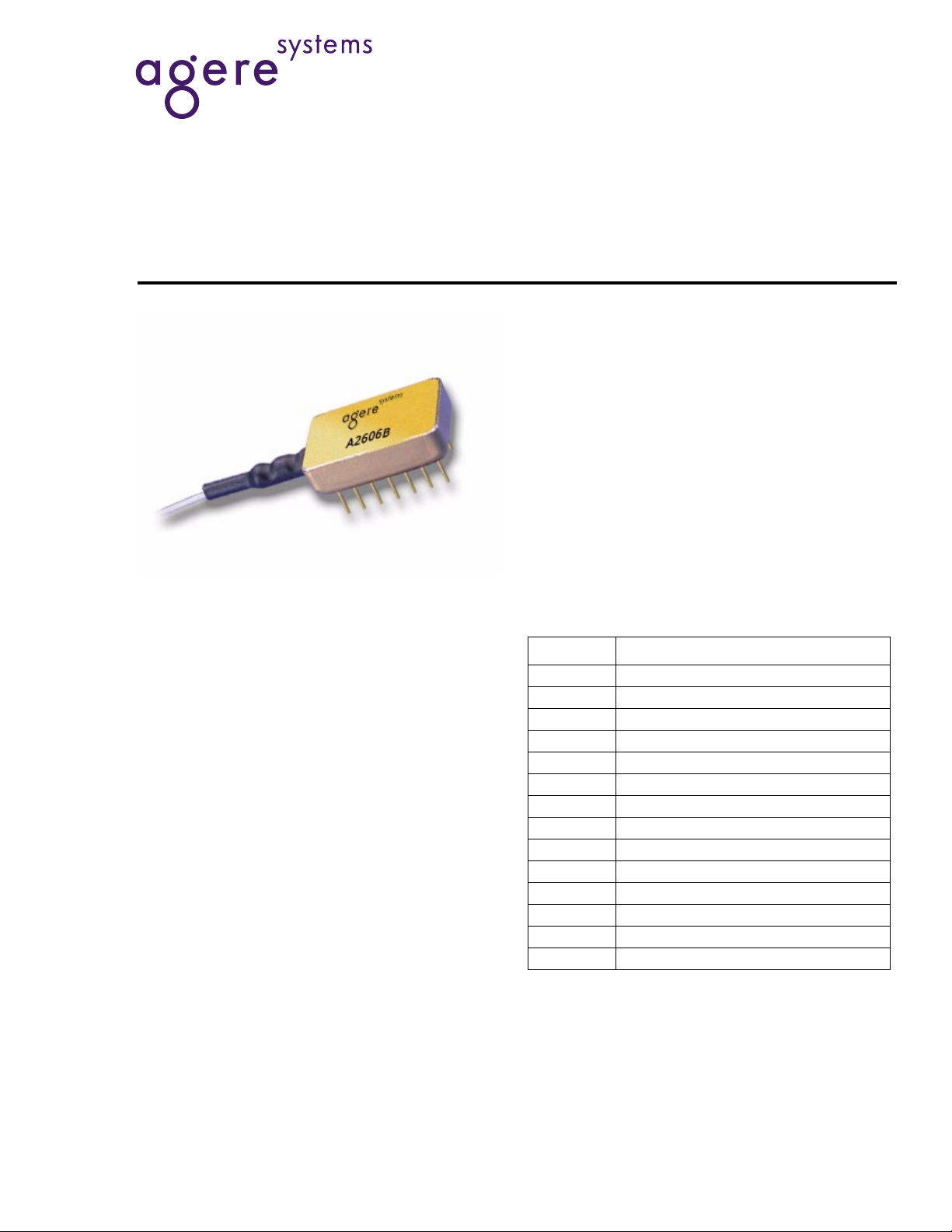
2606B Return-Path Photodiode Receiver Module
Description
The 2606B CA TV return-path photodiode module is a
critical component for the delivery of high-performance interactive services for today's two-way fiberoptic networks. These modules utilize PIN InGaAs
photodiodes in robust 14-pin DIL packages that
exhibit excellent sensitivity, low noise, and exceptional linearity in return-path optical links. The module incorporates a patented impedance-matching
circuit, which optimizes very low noise gain in optical
broadband receivers.
Data Sheet
August 2000
Features
■
5 MHz—200 MHz frequency range
■
Flat response to ± 0.5 dB
■
High optical responsivity
■
Ultra low optical return loss
75
■
impedance-matched
Ω
Applications
Return-path CATV receivers
■
Pin Information
Table 1. Pin Descriptions
Pin No. Description
1 2606A/B
2 Ground
3 Ground
4 Ground
5 Ground
6 Ground
7Open
8Open
9RF Out
10 Ground
11 Bias
12 Ground
13 Open
14 Ground
Data Sheet
2606B Return-Path Photodiode Receiver Module August 2000
Absolute Maximum Ratings
Stresses in excess of the absolute maximum ratings can cause permanent damage to the device. These are absolute stress ratings only. Functional operation of the device is not implied at these or any other conditions in excess
of those given in the operational sections of the data sheet. Exposure to absolute maximum ratings for extended
periods can adversely affect device reliability.
Parameter Symbol Min Max Unit
Operating Temperature Range T
OP
–40 85
Storage Temperature Range Tstg –40 85
Optical Input Power P
IN
—2
C
°
C
°
mW
(for continuous
operation)
dc Bias Voltage V
PD
—20V
Characteristics
Table 2. Electrical/Optical Characteristics
Parameter Symbol Min Typ Max Unit
Optical Return Loss RL 45 — — dB
Optical Wavelength Range
λ
Responsivity — —
— 1310 ± 10 — nm
—
>0.85 at 1310 nm,
>0.95 at 1550 nm
—
—
mA/mW
mA/mW
Bias Voltage — — 15 (nominal) — V
Table 3. RF Characteristics
Parameter Symbol Min Typ Max Unit
Frequency Range F 5 — 200 MHz
1
Gain
Flatness
2
Second-Order Distortion
3
G—8—dB
— — ±0.5 — dB
CSO — –65 — dBc
Third-Order Distortion CTB — –75 — dBc
1. Current gain of internal transformer.
2. Measured into 75 Ω load.
3. Two laser test. Each laser has 40% modulation index. Total received optical power is 0 dBm.
2
Agere Systems Inc.
 Loading...