

AGERE 2417K4A Datasheet
Data Sheet, Rev. 1
August 2001
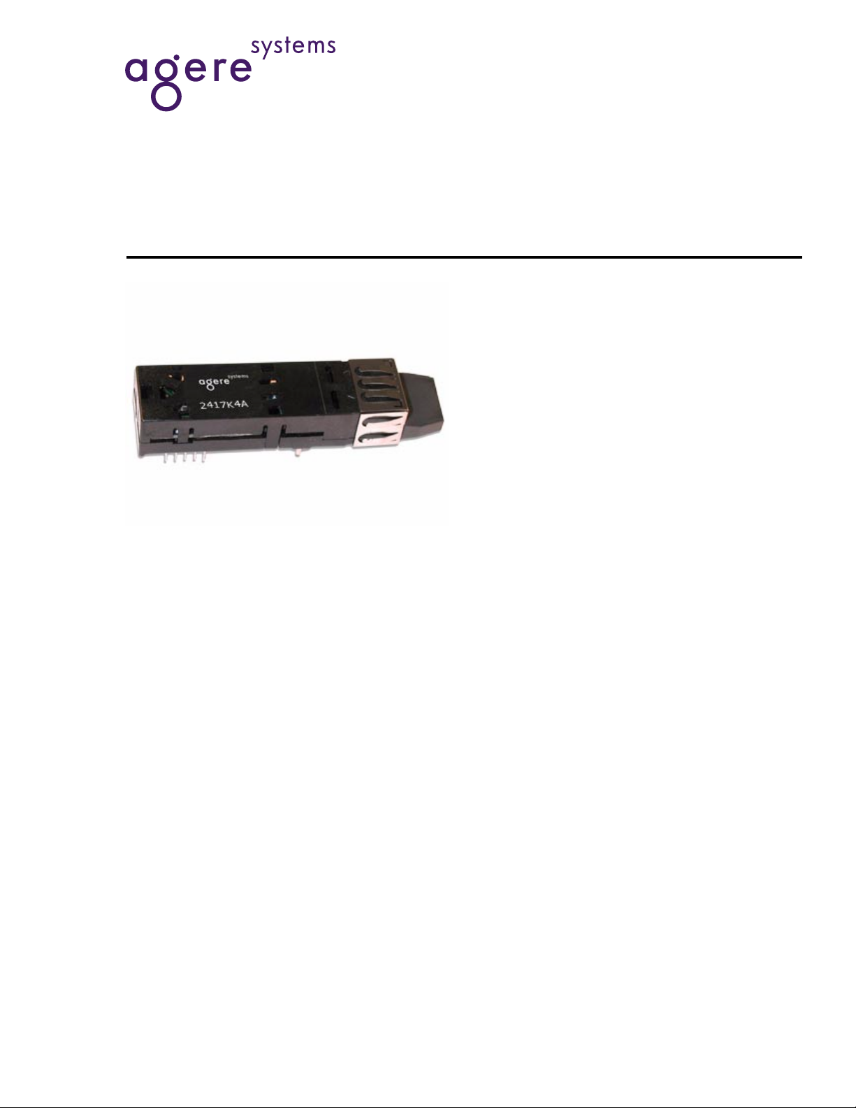
NetLight
®
2417K4A 1300 nm Laser
2.5 Gbits/s Transceiver
Available in a smal l form-factor, RJ-45 size, plastic packa ge,
the 2417K4A Transcei ver is a high-performance, cost-effective, optical transceiver for SONET appli cations.
Features
■
SONET SR OC-48, SDH I-16 applications
■
High-speed, optical data in terface f or shel f-t o-shel f
interconnect
■
Small form factor, RJ-45 size, 10-pin package
■
LC duplex receptacle
■
Uncooled 1300 nm laser transmitter with automatic
output power control
■
TTL signal-detect output
■
Low power dissipation
■
Single 3.3 V power supply
■
LVPECL/CML compatible data inputs and CML
compatible data outputs
■
Operating temperature range: 0 °C to
70 °C
■
Agere Systems Inc. Reliability and Qualification
Program for built-in quality and reliability
Description
The 2417K4A transceiv er i s a hi gh- speed, cost-effective optical transceiver intended for 2.488 Gbits/s
shelf-to-shelf optical interconnect appli cations as well
as SONET SR OC-48 and SDH I-16. The transceiver
features proven Agere Systems optics and is packaged in a narrow-width plastic housing with an LC
duplex receptacle. The receptacle fits into an RJ-45
form factor outline. The 10-pin package pinout conforms to a multisource transceiver agreement.
The transmitter f eatures the abil ity to interf ace to both
LVPECL and CML differential logic level data inputs.
It also features a TTL logic level disable input. The
receiver features differential CML logic level outputs
and a TTL logic level signal-detect output.
■
Transmitter disable input
■
Wide dynamic range receiver with InGaAs PIN
photodetector
NetLight
2417K4A 1300 nm Laser Data Sheet, Rev. 1
2.5 Gbits/s Transceiver August 2001
Absolute Maximum Rat ings
Stresses in excess of the absolute maximum ratings can cause permanent damage to the device. These are absolute stress ratings only. Functional operation of the device is not implied at these or any other conditions in excess
of those given in the operations sections of the data sheet. Exposure to absolute maximum ratings for extended
periods can adversely affect device reliability.
Parameter Symbol Min Max Unit
Supply Voltage V
Operating Case Temperature Range T
Storage Temperature Range T
CC
stg
05V
C
070°C
–40 85 °C
Lead Soldering Temperature/Time — — 250/10 °C/s
Operating Wavelength Range λ 1.1 1.6 µm
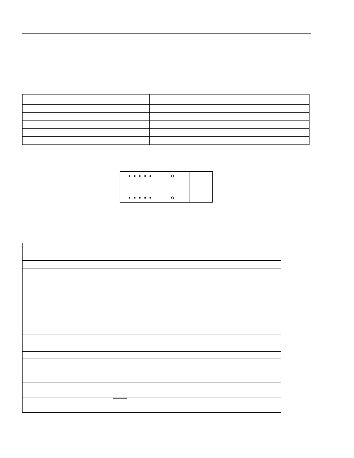
Pin Information
Figure 1. 2417K4A Transceiver, 10-Pin Configuration, Top View
Table 1. Transceiver Pin Descriptions
Pin
Number
MS MS
Symbol Name/Description
Mounting Studs.
mechanical attachment to the circuit board. The y ma y also provi de an
optional connection of the transceiver to the equipment chassis
ground.
1V
2V
EER
CCR
3SD
Receiver Signal Ground.
Receiver Power Supply.
Signal Detect.
Normal operation: logic one output.
Fault condition: logic zero output.
4RD–
5RD+
6V
7V
8T
CCT
EET
DIS
9TD+
Received
DATA
Received DATA Out.
Transmitter Power Supply.
Transmitter Signal Ground.
Transmitter Disable.
Transmitter DATA In
sisting of a 100 Ω resistor between the TD+ and TD– pins.
10 TD–
Transmitter
DATA
12345
109876
RX
TX
Receiver
The mounting studs are provided for transceiver
Out.
Transmitter
. An internal 50 Ω termination is provided, con-
In
. See TD+ pin for terminations. LVPECL
1-967
Logic
Family
NA
NA
NA
LVTTL
CML
CML
NA
NA
LVTTL
LVPECL
or CML
or CML
2 Agere Systems Inc.
Data Sheet, Rev. 1
DATA
SINGLE ENDE D
V
OH
V
OL
DATA
V
OH
V
OL
DIFFERENTIAL
NetLight
2417K4A 1300 nm Laser
August 2001 2.5 Gbits/s Transceiver
Electrostatic Discharge
Caution: This device is susceptible to damage as
a result of electrostatic discharge (ESD).
Take proper precautions during both
handling and testing. Follow
dard
EIA
-625.
EIA
®
Stan-
Although protection circuitry is designed into the
device, take proper precautions to avoid exposure to
ESD.
Agere Systems employs a human-body model (HBM)
for ESD susceptibility testing and protection-design
evaluation. ESD voltage thresholds are dependent on
the critical parameters used to define the model. A
standard HBM (resistance = 1.5 kΩ, capacitance =
100 pF) is widely used and, therefore, can be used for
comparison purposes. The HBM ESD threshold
established for the 2417K4A transceiver is ±1000 V.
Application Information
The 2417 receiver section is a highly sensitive fiberoptic receiver. Although the data outputs are digital
logic levels (CML), the device should be thought of as
an analog component. When laying out system application boards, the 2417 transceiver should receive the
same type of consideration one would give to a sensitive analog component.
Printed-Wiring Board Layout Considerations
A fiber-optic receiver employs a very high gain, widebandwidth transimpedance amplifier. This amplifier
detects and amplifies signals that are only tens of nA in
amplitude when the receiver is operating near its sensi tivity limit. Any unwanted signal currents that couple
into the receiver circuitry cause a decrease in the
receiver's sensitivity and can also degrade the performance of the receiver's signal detect (SD) circuit. To
minimize the coupling of unwanted noise into the
receiver, careful attention must be given to the printedwiring board.
Multilayer construction also permits the routing of sensitive signal traces away from high-level, high-speed
signal lines. To minimize the possibility of coupling
noise into the receiver section, high-level, high-speed
signals such as transmitter inputs and clock lines
should be routed as far away as possible from the
receiver pins.
Noise that couples into the receiver through the power
supply pins can also degrade performance. It is
recommended that a pi filter, shown in Figure 3, be
used for both the transmitter and receiver power
supplies.
Data and Signal Detect Outputs
Due to the high switching speeds of CML outputs,
transmission line design must be used to interconnect
components. To ensure optimum signal fidelity, both
data outputs (RD+/RD–) should be terminated identically. The signal lines connecting the data outputs to
the next device should be equal in length and have
matched impedances. Controlled impedance stripline
or microstrip construction must be used to preserve the
quality of the signal into the next component and to
minimize reflections bac k int o the receiver, which could
degrade its performance. Excessive ringing due to
reflections caused by improperly terminated signal
lines makes it difficult for the component receiving
these signals to decipher the proper logic levels and
can cause transitions to occur where none were
intended. Also, by minimizing high-frequency ringing,
possible EMI problems can be avoided.
The signal-detect output is positiv e LVTTL logic. A logic
low at this output indicates that the optical signal into
the receiver has been interrupted or that the light level
has fallen below the minimum signal-detect threshold.
This output should not be used as an error rate indicator, since its switching threshold is determined only by
the magnitude of the incoming optical signal.
At a minimum, a double-sided printed-wiring board
(PWB) with a large component-side ground plane
beneath the transceiver must be used. In applications
that include many other high-speed devices, a multilayer PWB is highly recommended. This permits the
placement of power and ground on separate layers,
which allows them to be isolated from the signal lines.
Agere Systems Inc. 3
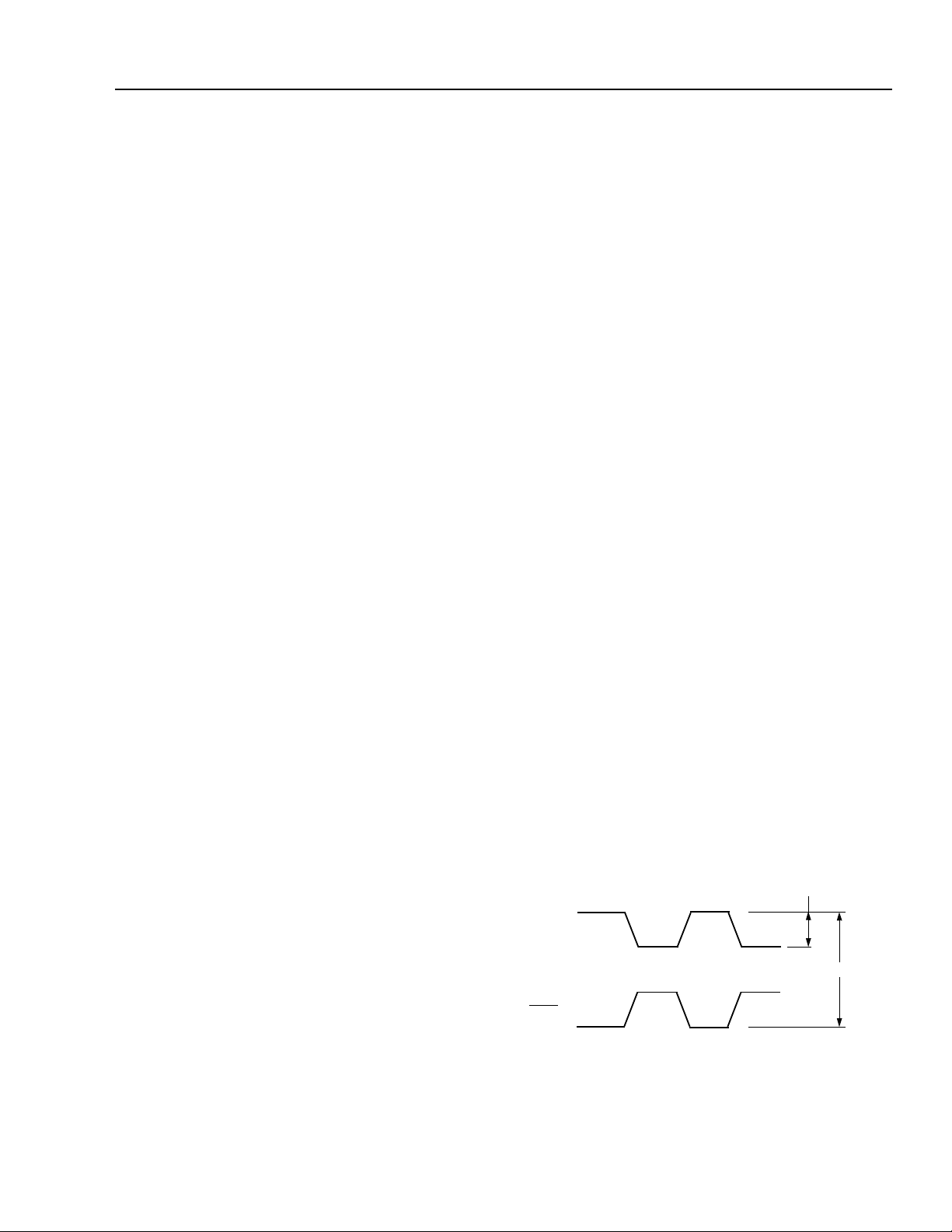
Figure 2. Data Input/Output Logic Level Definitions

NetLight
2417K4A 1300 nm Laser Data Sheet, Rev. 1
2.5 Gbits/s Transceiver August 2001
Application Information
(continued)
Transceiver Processing
When the process plug is placed in the transceiver's optical port, the transceiver and plug can withstand normal
wave soldering and aqueous spray cleaning processes. However, the transceiver is not hermetic, and should not
be subjected to immersion in cleaning solvents. The transceiver case should not be exposed to temperatures in
excess of 125 °C. The transceiver pins can be wave soldered at 250 °C for up to 10 seconds. The process plug
should only be used once. After rem ovi ng the process plug fr om the tr ansceiv er, it m ust not be used agai n as a process plug; however, if it has not been contaminated, it can be reused as a dust cover.
Transceiver Optical and Electrical Characteristics
Table 2. Transmitter Optical and Electrical Characteristics
Parameter Symbol Min Max Unit
Average Optical Output Power (EOL) P
Optical Wavelength λ
Spectral Width ∆λ
Dynamic Extinction Ratio EXT 8.2 — dB
Output Optical Eye Compliant with SONET GR-253-CORE and
Power Supply Current I
Input Data Voltage:
Single Ended*
Differential*
Transmit Disable Voltage
Transmit Enable Voltage
* 50 ¾ load, measured single ended. Differential operation is necessary for optimum performance. (See Figure 2 for visual representation.)
† TTL compatible interface.
†
†
(T
= 0 °C to 70 °C; VCC = 3.135 V—3.465 V)
C
O
C
RMS
–10.0 –3.0 dBm
1266 1360 nm
—4nm
ITU-T G.957 Eye Mask Requirements
V
V
CCT
INp-p
INp-p
V
EN
V
D
—190mA
150
300
VCC – 0.9 V
EE
V
800
1600
CC
VEE + 0.8 V
mVp-p
mVp-p
V
Table 3. Receiver Optical and Electrical Characteristics
= 0 °C to 70 °C; VCC = 3.135 V—3.465 V)
(T
C
Parameter Symbol Min Max Unit
Average Sensitivity:*
MAX
CCR
I
— –18 dBm
–3 — dBm
— 110 mA
800 mV (CML) Differential Input To Transmitter P
Maximum Input Power* P
Power Supply Current I
Output Data Voltage:
Single Ended
Differential
†
†
OUTp-p
V
OUTp-p
V
300
600
500
1000
mVp-p
mVp-p
Signal-detect Switching Threshold:
Assert
Deassert
LST
LST
D
I
–45
—
–19
–18.5
dBm
dBm
Signal-detect Hysteresis HYS 0.5 6 dB
Signal-detect Voltage:
Low
High
‡
OL
V
OH
V
0.0
2.4
0.8
V
CC
V
V
Signal-detect Response Time SDRT — 100 µs
* 223 – 1 PRBS with a BER of 1 x 10
† 50 ¾ load, measured single ended. Differential operation is necessary for optimum performance.(See Figure 2 for visual representation.)
‡ TTL compatible interface.
–10
.
4 Agere Systems Inc.
 Loading...