

AGERE 1430G5LL Datasheet
®
NetLight
1430G5 Type SONET/SDH
Long-Reach Transceivers with Clock Recovery
■
Wide dynamic range receiver with InGaAs PIN
photodetector
■
LVTTL signal-detect output
■
Low power dissipation
■
Raised ECL (LVPECL) logic data interfaces
■
Operating case temperature range: –40 °C to
+85 °C
■
Agere Systems Inc. Reliability and Qualification
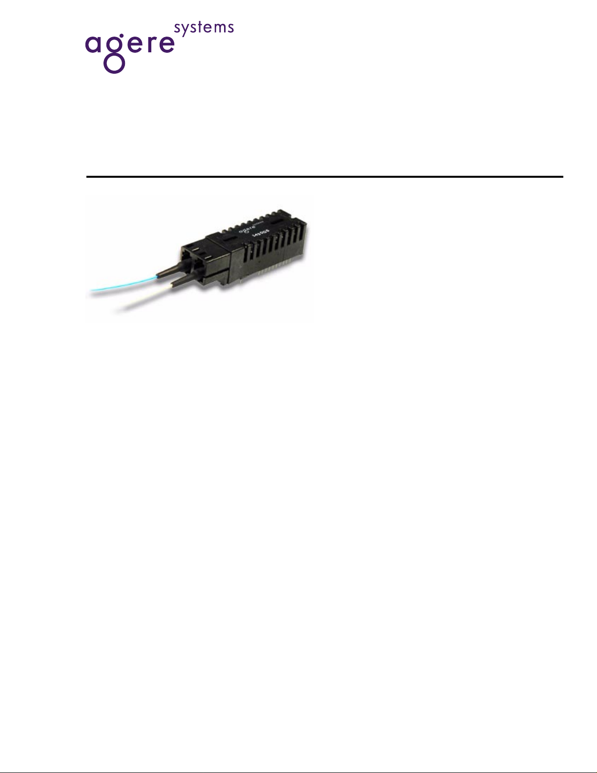
Available in a small form factor, plastic package, the
1430G5 are high-performance, cost-effective transceivers for
SONET/SDH long-reach applications at 155 Mbits/s.
Program for built-in quality and reliability
Description
Data Sheet, Rev 1.
August 2001
Features
■
SONET LR-1/SDH L1.1 Compliant (ITU-T G.957
Specifications)
■
Small form factor, RJ-45 size, multisourced 20-pin
package
■
Requires single 3.3 V power supply
■
Clock recovery
■
Fiber pigtail
■
Uncooled 1300 nm laser transmitter with automatic
output power control
■
Transmitter disable input
■
Analog alarm outputs
The 1430G5-Type transceiver is a high-speed, costeffective optical transceiver that is compliant with the
International Telecommunication Union Telecommunication (ITU-T) G.957 specifications for use in
SONET and SDH long-reach applications. The
1430G5 operates at the OC-3/STM-1 rate of
155 Mbits/s. The transceiver features Agere Systems’ optics and is packaged in a narrow-width plastic housing with two 1 meter fiber pigtails terminated
with LC connectors. The 20-pin package and pinout
conform to a multisource transceiver agreement.
The transmitter features differential LVPECL logic
level data inputs, a LVTTL logic level disable input.
The receiver features differential LVPECL logic level
data and cl ock outputs, and a LVTTL logic level
signal-detect output.
NetLight
Long-Reach Transceivers with Clock Recovery
1430G5 Type SONET/SDH
Data Sheet, Rev 1.
August 2001
Absolute Maximum Ratings
Stresses in excess of the absolute maximum ratings can cause permanent damage to the device. These are absolute stress ratings only. Functional operation of the device is not implied at these or any other conditions in excess
of those given in the operations sections of the data sheet. Exposure to absolute maximum ratings for extended
periods can adversely affect device reliability.
Parameter Symbol Min Max Unit
Supply Voltage V
Operating Case Temperature Range T
Storage Case Temperature Range T
CC
C
stg
03.6V
–40 85 °C
–40 85 °C
Lead Soldering Temperature/Time — — 250/10 °C/s
Operating Wavelength Range λ 1.1 1.6 nm
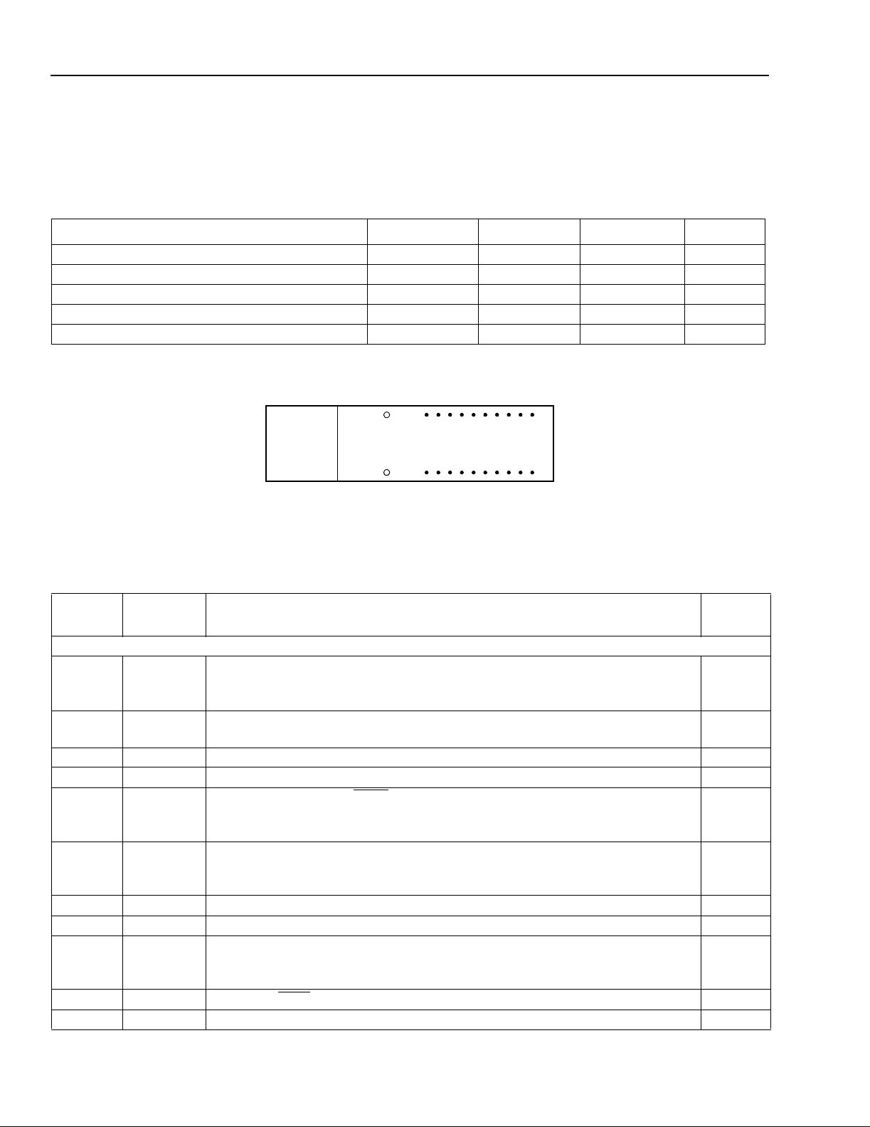
Pin Information
Figure 1. 1430G5 and 1430H5-Type Transceivers, 20-Pin Configuration, Top View
Table 1. Transceiver Pin Descriptions
Pin
Number
MS MS
Symbol Name/Description
Mounting Studs.
cal attachment to the circuit board. They may also provide an optional connection of the transceiver to the equipment chassis ground.
1 Photode-
Photodetector Bias.
tector Bias
2V
3V
EER
EER
4CLK–
Receiver Signal Ground.
Receiver Signal Ground.
Received Recovered
the received data output. The falling edge occurs in the middle of the received
data bit period.
5CLK+
Received Recovered Clock Out.
of the received data output. The rising edge occurs in the middle of the
received data bit period.
6V
7V
EER
CCR
8SD
Receiver Signal Ground.
Receiver Power Supply.
Signal Detect.
Normal operation: logic one output.
Fault condition: logic zero output.
9 RD–
10 RD+
Received
Received DAT A Out.
DATA
TX
RX
20 19 18 17 16
20-PIN MODULE - TOP VIEW
12345
15 1413 12 11
678910
Receiver
The mounting studs are provided for transceiver mechani-
This lead supplies bias for the PIN photodetector diode. NA
Out.
Clock
The rising edge occurs at the rising edge of
The falling edge occurs at the rising edge
Out.
No Internal terminations will be provided. LVPECL
No internal terminations will be provided. LVPECL
1-967(F).b
Logic
Family
NA
NA
NA
LVPECL
LVPECL
NA
NA
LVTTL
2 Agere Systems Inc.

Data Sheet, Rev 1.
August 2001
NetLight
1430G5 Type SONET/SDH
Long-Reach Transceivers with Clock Recovery
Pin Information
(continued)
Table 1. Transceiver Pin Descriptions
Pin
Number
11 V
12 V
13 T
14 TD+
15 TD–
16 V
17 Bmon–
Symbol Name/Description
CCT
EET
DIS
Transmitter Power Supply.
Transmitter Signal Ground.
Transmitter Disable.
Transmitter DATA In.
Transmitter DATA In Bar.
EET
Transmitter Signal Ground.
Laser Diode Bias Current Monitor—Negative End.
is accessible as a dc-voltage by measuring the voltage developed across pins
17 and 18.
18 B
19 P
MON
MON
Laser Diode Bias Current Monitor—Positive End.
+
Laser Diode Optical Power Monitor—Negative End.
–
monitor current is accessible as a dc-voltage by measuring the voltage devel-
oped across pins 19 and 20.
20 P
MON
Laser Diode Optical Power Monitor—Positive End.
+
(continued)
LVPECL
Transmitter
Logic
Family
NA
NA
LVTTL
LVPECL
NA
The laser bias current
NA
See pin 17 description. NA
The back-facet diode
NA
See pin 19 description. NA
Electrostatic Discharge
Caution: This device is susceptible to damage as
a result of electrostatic discharge (ESD).
Take proper precautions during both
handling and testing. Follow
dard
EIA
-625.
EIA
®
Stan-
Although protection circuitry is designed into the
device, take proper precautions to avoid exposure to
ESD .
Agere Systems employs a human-body model (HBM)
for ESD-susceptibility testing and protection-design
evaluation. ESD voltage thresholds are dependent on
the critical parameters used to define the model. A
standard HBM (resistance = 1.5 kΩ, capacitance =
100 pF) is widely used and, therefore, can be used for
comparison purposes. The HBM ESD threshold established for the 1430G5 transceiver is ±1000 V.
Application Information
The 1430 receiver section is a highly sensitive fiberoptic receiver. Although the data outputs are digital
logic levels (LVPECL), the device should be thought of
as an analog component. When laying out system
application boards, the 1430 transceiver should receive
the same type of consideration one would give to a
sensitive analog component.
Printed-Wir ing Board Layout Cons iderations
A fiber-optic receiver employs a very high gain, wide
bandwidth transimpedance amplifier. This amplifier
detects and amplifies signals that are only tens of nA in
amplitude when the receiver is operating near its sensitivity limit. Any unwanted signal currents that couple
into the receiver circuitry cause a decrease in the
receiver's sensitivity and can also degrade the performance of the receiver's signal detect (SD) circuit. To
minimize the coupling of unwanted noise into the
receiver, careful attention must be given to the printedwiring board.
At a minimum, a double-sided printed-wiring board
(PWB) with a large component-side ground plane
beneath the transceiver must be used. In applications
that include many other high-speed devices, a multilayer PWB is highly recommended. This permits the
placement of power and ground on separate layers,
which allows them to be isolated from the signal lines.
Multilayer construction also permits the routing of sensitive signal traces away from high-level, high-speed
signal lines. To minimize the possibility of coupling
noise into the receiver section, high-level, high-speed
signals such as transmitter inputs and clock lines
should be routed as far away as possible from the
receiver pins.
Agere Systems Inc. 3
 Loading...