

AGERE 1417H5A, 1417G5A Datasheet
®
NetLight
1417G5 and 1417H5-Type
ATM/SONET/SDH Transceivers with Clock Recovery
■
Transmitter dis able input
■
Wide dynamic range receiver with InGaAs PIN
photodetector
■
LVTTL signal-detect output
■
Low power dissipation
■
Raised ECL (PECL) logic data and clock interfaces
■
Operating case temperature range: –40 °C to
+85 °C
Data Sheet
January 2000
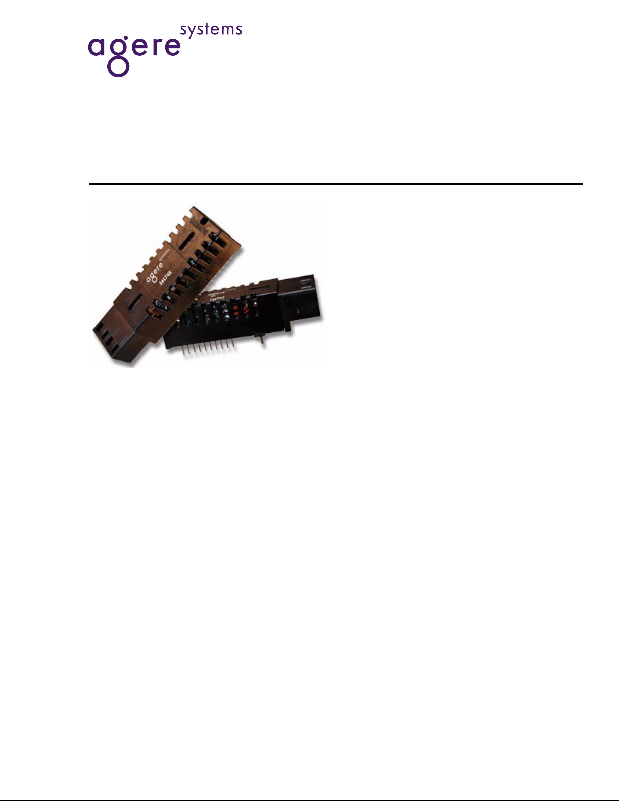
Avail a ble in a small form factor, RJ-45 size, plastic package,
the 1417G5 and 1417H5-Type are high-performance, costeffective transceivers for ATM/SONET/SDH applications at
155 Mbits/s and 622 Mbits/s.
Features
■
SONET/SDH Compliant (ITU-T G.957 Specifications)
— IR-1/S1.1, S4.1
■
Small form factor, RJ-45 size, multisourced 20-pin
package
■
Requires single 3.3 V power supply
■
Clock recovery
■
LC duplex receptacle
■
Analog alarm outputs
■
Uncooled 1300 nm laser transmitter with automatic
output power control
■
Agere Systems Inc. Reliability and Qualification
Program for built-in quality and reliability
Description
The 1417G5 and 1417H5 transceivers are highspeed, cost-effective optical transceivers that are
compliant with the International Telecommunication
Union Telecommunication (ITU-T) G.957 specifications for use in ATM, SONET, and SDH applications.
The 1417G5 operates at the OC-3/STM-1 rate of
155 Mbits/s, and the 1417H5 operates at the OC-12/
STM-4 rate of 622 Mbits/s. The transceiver features
Agere Systems high-reliability optics and is packaged in a narrow-width plastic housing with an LC
duplex receptacle. This receptacle fits into an RJ-45
form factor outline. The 20-pin package and pinout
conform to a multisource transceiver agreement.
The transmitter features differential PECL logic level
data inputs and a LVTTL logic level disable input. The
receiver features differential PECL logic level data
and clock outputs and a LVTTL logic level signaldetect output.
NetLight
1417G5 and 1417H5-Type Data Sheet
ATM/SONET/SDH Transceivers with Clock Recovery January 2000
Absolute Maximum Ratings
Stresses in excess of the absolute maximum ratings can cause permanent damage to the device. These are absolute stress ratings only. Functional operation of the device is not implied at these or any other conditions in excess
of those given in the operations sections of the data sheet. Exposure to absolute maximum ratings for extended
periods can adversely affect device reliability.
Parameter Symbol Min Max Unit
Supply Voltage V
Operating Case Temperature Range T
Storage Case Temperature Range T
CC
C
stg
03.6V
–40 85 °C
–40 85 °C
Lead Soldering Temperature/Time — — 250/10 °C/s
Operating Wavelength Range λ 1.1 1.6 nm
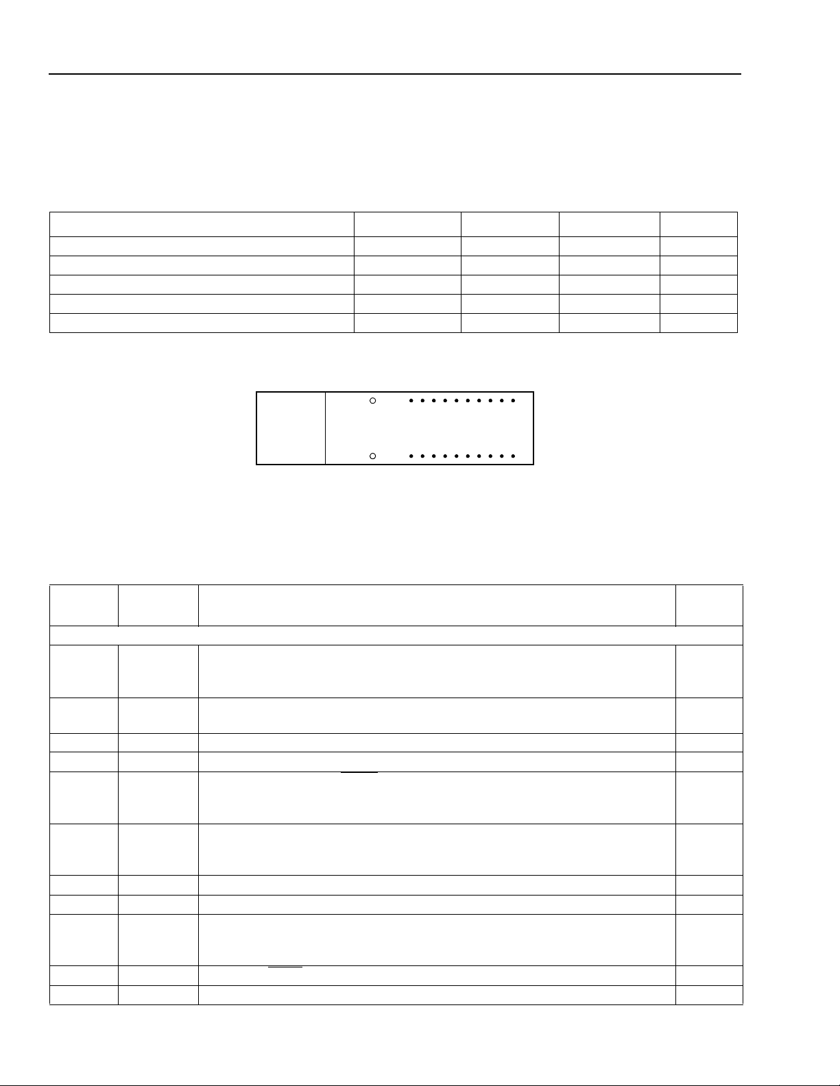
Pin Information
Figure 1. 1417G5 and 1714H5 Transceivers, 20-Pin Configuration, Top View
Table 1. Transceiver Pin Descriptions
Pin
Number
MS MS
Symbol Name/Description
Mounting Studs.
cal attachment to the circuit board. They may also provide an optional connection of the transceiver to the equipment chassis ground.
1 Photode-
Photodetector Bias.
tector Bias
2V
3V
EER
EER
4CLK–
Receiver Signal Ground.
Receiver Signal Ground.
Received Recovered Clock
the received data output. The falling edge occurs in the middle of the received
data bit period.
5CLK+
Received Recovered Clock Out.
of the received data output. The rising edge occurs in the middle of the
received data bit period.
6V
7V
EER
CCR
8SD
Receiver Signal Ground.
Receiver Power Supply.
Signal Detect.
Normal operation: logic one output.
Fault condition: logic zero output.
9 RD–
10 RD+
Received DATA
Received DATA Out.
TX
RX
20 19 18 17 16
20-PIN MODULE - TOP VIEW
12345
15 14 13 12 11
678910
Receiver
The mounting studs are provided for transceiver mechani-
This lead supplies bias for the PIN photodetector diode. NA
Out.
The rising edge occurs at the rising edge of
The falling edge occurs at the rising edge
Out.
No internal terminations will be provided. PECL
No internal terminations will be provided. PECL
1-967(F).b
Logic
Family
NA
NA
NA
PECL
PECL
NA
NA
LVTTL
2
Agere System s Inc.

Data Sheet
NetLight
1417G5 and 1417H5-Type
January 2000 ATM/SONET/SDH Transceivers with Clock Recovery
Pin Information
(continued)
Table 1. Transceiver Pin Descriptions
Pin
Number
11 V
12 V
13 T
14 TD+
15 TD–
16 V
17 B
Symbol Name/Description
CCT
EET
DIS
Transmitter Power Supply.
Transmitter Signal Ground.
Transmitter Disable.
Transmitter Data In
Transmitter Data In Bar
EET
MON
Transmitter Signal Ground.
Laser Diode Bias Current Monitor—Negative End.
(–)
is accessible as a dc-voltage by measuring the voltage developed across pins
17 and 18.
18 B
19 P
MON
MON
Laser Diode Bias Current Monitor—Positive End.
(+)
Laser Diode Optical Power Monitor—Negative End.
(–)
monitor current is accessible as a dc-voltage by measuring the voltage devel-
oped across pins 19 and 20.
Laser Diode Optical Power Monitor—Positive End.
20 P
MON
(+)
(continued)
Transmitter
. PECL
. PECL
The laser bias current
See pin 17 description. NA
The back-facet diode
See pin 19 description. NA
Logic
Family
NA
NA
LVTTL
NA
NA
NA
Electrostatic Discharge
Caution: This device is susceptible to damage as
a result of electrostatic discharge (ESD).
Take proper precautions during both
handling and testing. Follow
dard
EIA
-625.
EIA
®
stan-
Although protection circuitry is designed into the
device, take proper precautions to avoid exposure to
ESD. Agere Systems employs a human-body model
(HBM) for ESD-susceptibility testing and protectiondesign evaluation. ESD voltage thresholds are dependent on the critical parameters used to define the
model. A standard HBM (resistance = 1.5 kΩ, capaci-
tance = 100 pF) is widely used and, therefore, can be
used for comparison purposes. The HBM ESD threshold established for the 1417G5 and 1417H5 transceivers is ±1000 V.
Application Information
The 1417 receiver section is a highly sensitive fiberoptic receiver. Although the data outputs are digital
logic levels (PECL), the device should be thought of as
an analog component. When laying out system application boards, the 1417 transceiver should receive the
same type of consideration one would give to a sensitive analog component.
Printed-Wiring Board Layout Considerations
A fiber-optic receiver employs a very high-gain, widebandwidth transimpedance amplifier. This amplifier
detects and amplifies signals that are only tens of nA in
amplitude when the receiver is operating near its sensitivity limit. Any unwanted signal currents that couple
into the receiver circuitry cause a decrease in the
receiver's sensitivity and can also degrade the performance of the receiver's signal detect (SD) circuit. To
minimize the coupling of unwanted noise into the
receiver, careful attention must be given to the printedwiring board.
At a minimum, a double-sided printed-wiring board
(PWB) with a large component-side ground plane
beneath the transceiver must be used. In applications
that include many other high-speed devices, a multilayer PWB is highly recommended. This permits the
placement of power and ground on separate layers,
which allows them to be isolated from the signal lines.
Multilayer construction also permits the routing of sensitive signal traces away from high-level, high-speed
signal lines. To minimize the possibility of coupling
noise into the receiver section, high-level, high-speed
signals such as transmitter inputs and clock lines
should be routed as far away as possible from the
receiver pins.
Agere Systems Inc.
3

NetLight
1417G5 and 1417H5-Type Data Sheet
ATM/SONET/SDH Transceivers with Clock Recovery January 2000
Application Information
(continued)
Noise that couples into the receiver through the power
supply pins can also degrade performan ce. It is recommended that the pi filter, shown in Figure 2, be used for
both the transmitter and receiver power supplies.
Data Clock and Signal Detect Outputs
The data clock and signal detect outputs of the 1417
transceiver are driven by open-emitter NPN transistors,
which have an output impedance of approximately 7 Ω.
Each output can provide approximately 50 mA maximum curr ent to a 50 Ω load terminated to V
Due to the high switching speeds of ECL outputs,
transmission line design must be used to interconnect
components. To ensure optimum signal fidelity, both
data outputs (RD+/RD–) and clock outputs (CLK+/
CLK–) should be terminated identically. The signal
lines connecting the data and clock outputs to the next
device should be equal in length and have matched
impedances. Controlled impedance stripline or microstrip construction must be used to preserve the quality
of the signal into the next component and to minimize
reflections back into the receiver, which could degrade
its performance. Excessive ringing due to reflections
caused by improperly terminated signal lines makes it
difficult for the component receiving these signals to
– 2.0 V.
CC
decipher the proper logic levels and can cause transitions to occur where none were intended. Also, by minimizing high-frequency ringing, possible EMI problems
can be avoided.
The signal-detect output is LVTTL logic. A logic low at
this output indicates that the optical signal into the
receiver has been interrupted or that the light level has
fallen below the minimum signal detect threshold. This
output should not be used as an error rate indicator,
since its switching threshold is determined only by the
magnitude of the incoming optical signal.
Transceiver Processing
When the process plug is placed in the transceiver's
optical por t, the transce iver and plug can withst and
normal wave soldering and aqueous spray cleaning
processes. However, the transceiver is not hermetic,
and should not be subjected to immersion in cleaning
solvents. The transceiver case should not be exposed
to temperatures in excess of 125 °C. The transceiver
pins can be wave soldered at 250 °C for up to 10 sec-
onds. The process plug should only be used once.
After removing the process plug from the transceiver, it
must not be us ed agai n as a proc ess pl ug; h ow e v er, if it
has not been contaminated, it can be reused as a dust
cover.
Transceiver Optical and Electrical Characteristics
Table 2. Transmitter Optical and Electrical Characteristics
Parameter Symbol Min Max Unit
Average Optical Output Pow er (EOL) P
Optical Wavelength:
STM-1 (4 nm spectral width, maximum)
STM-4 (2.5 nm spectral width, maximum)
Dynamic Extinction Ratio EXT 8.2 — dB
Power Supply Current I
Input Data Voltage:
Low
High
Transmit Disable Voltage V
Transmit Enable Voltage V
Laser Bias Voltage V
Laser Back-facet Monitor Voltage V
(T
= –40 °C to +85 °C; VCC = 3.135 V to 3.465 V)
C
O
λ
C
CCT
V
IL
V
IH
D
EN
BIAS
BF
–15.0 –8.0 dBm
1261
1274
1360
1356
— 150 mA
VCC – 1.81
V
– 1.025
CC
VCC – 1.3 V
V
EE
– 1.62
V
CC
V
– 0.88
CC
CC
VEE + 0.8 V
00.70V
0.01 0.20 V
nm
nm
V
V
V
4
4
Agere System s Inc.
 Loading...