

AGERE 1345TNPD, 1345TNPC, 1345TMPD, 1345TMPC, 1345TBPD Datasheet
...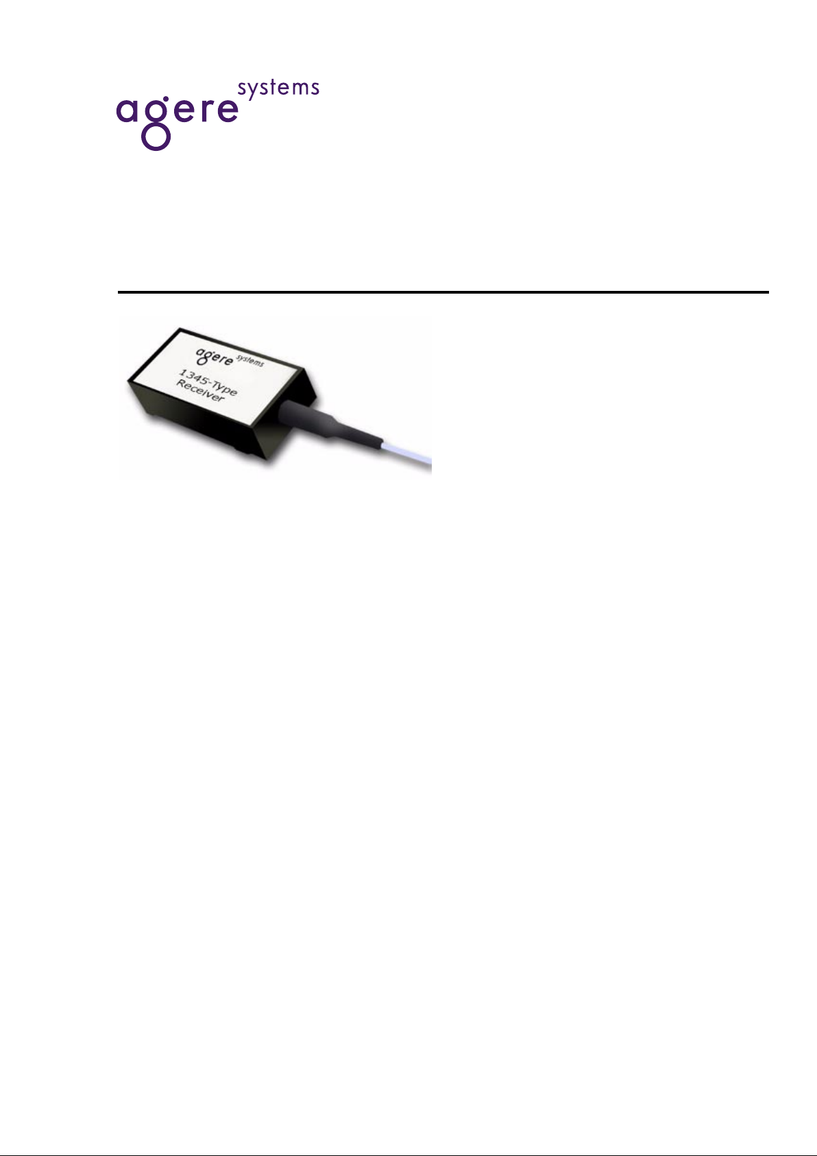
1345-Type Receiver with
Clock Recovery and Data Retiming
Data Sheet
January 2000
Operating at 1.3 µm or 1.55 µm wavelengths and at
155 Mbits/s or 622 Mbits/s, the versatile 1345-T ype Receiver is
manufactured in a 20-pin, plastic DIP with a multimode fiber
pigtail.
Features
■
Backward compatible with 1330 family
■
Space-saving, self-contained, 20-pin plastic DIP
■
Silicon based ICs
■
Single 5 V power supply operation including
photocurrent monitor capability
■
Exceeds all SONET (GR-253-CORE) and ITU-T
G.958 jitter requirements
■
Clocked decision circuit
■
Regenerated differential clock signal
■
Wide dynamic range
■
Qualified to meet the intent of
Telcordia Technolo-
gies
™ reliability practices
■
Operates at data rates of 155 Mbits/s or
622 Mbits/s
■
Positive ECL (PECL) data outputs
■
CMOS (TTL) link-status flag output
■
Operation at 1.3 µm or 1.55 µm wavelengths
■
Operating temperature range of –40 °C to +85 °C
Applications
■
Telecommunications:
— Inter- and intraoffice SONET/ITU-T SDH
— Subscriber loop
— Metropolitan area networks
■
High-speed data communications
Description
The 1345-Type fiber-optic receiver is designed for
use in transmission systems or medium- to highspeed data communication applications. Used in
intermediate- and long-reach applications, the
receiver operates at the SONET OC-3 or OC-12 data
rate as well as the ITU-T synchronous digital hierarchy (SDH) rate of STM-1 or STM-4, depending on
the receiver model chosen. The receiver meets all
present
Telcordia Technologies
GR-253-CORE
requirements, the current ANSI T1X1.5 intraoffice
specifications, and the ITU-T G.957 and G.958 recommendations. Compact packaging, a high level of
integration, and a wide dynamic range make these
receivers ideal for data communications.
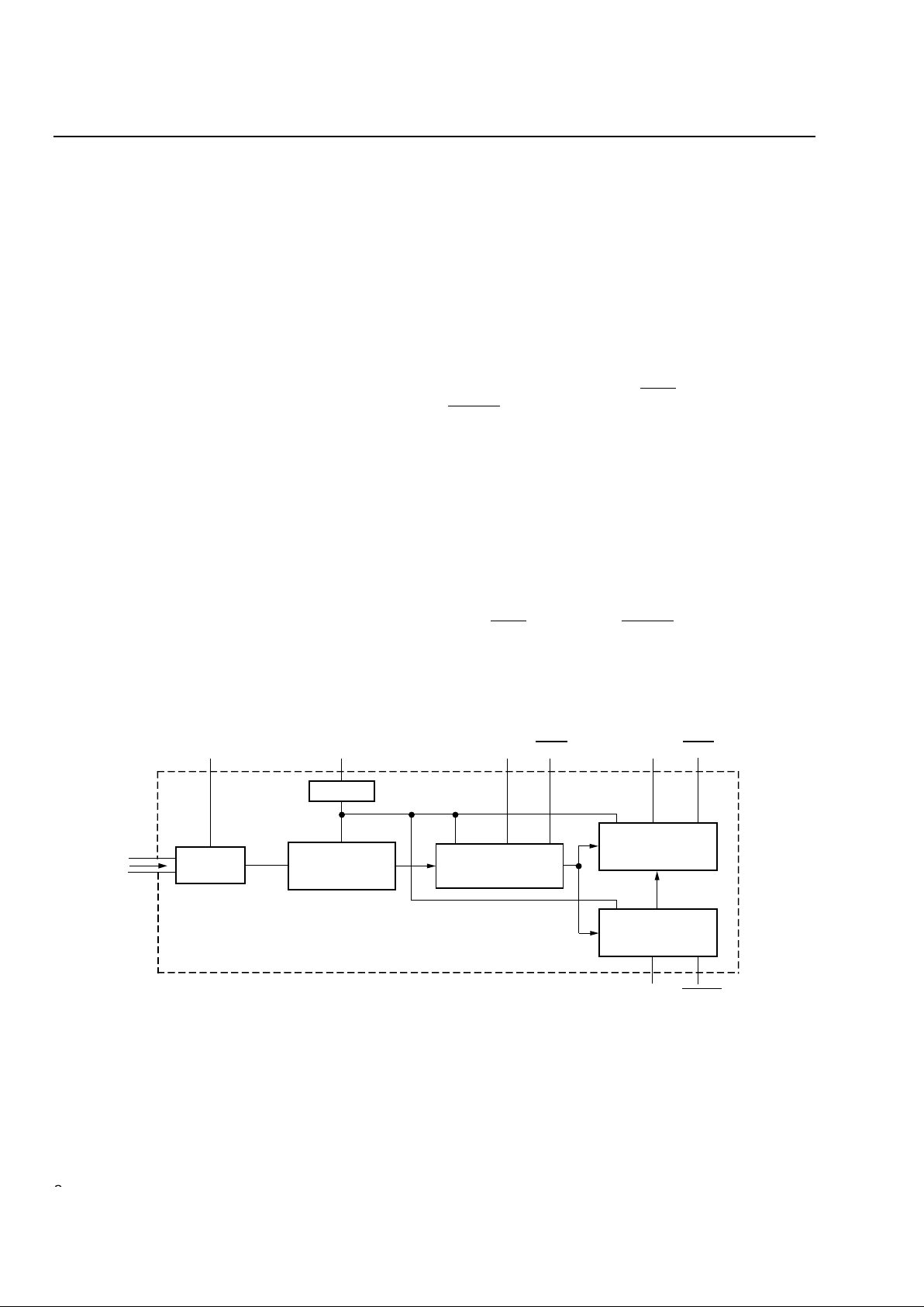
Manufactured in a 20-pin DIP, the receiver consists of
a planar InGaAs PIN photodetector, a silicon preamplifier, a silicon bipolar limiting amplifier that converts
the small signal to ECL levels, a timing recovery unit
to recover the clock, and a silicon bipolar decision circuit.
2
2
Agere Systems Inc.
1345-Type Receiver with Data Sheet
Clock Recovery and Data Retiming January 2000
Description
(continued)
The receiver converts optical signals in the range of
1.1 µm to 1.6 µm into retimed clock and data signals.
The clock and data outputs are raised-ECL (PECL)
logic levels. A CMOS-level flag output indicates when
there is a loss of optical signal.
The receiver requires a 5 V power supply for the amplifier, logic, and PLL CRC circuits. The operating case
temperature range is –40 °C to +85 °C.
Pin 10
Pin 10 on the 1345-Type receiver is not an internally
connected (NIC) pin. This definition allows the 1345 to
be used in most customer 20-pin receiver module
applications. Customer’s printed-wiring boards that are
designed with ground, +5 V, –5 V, or no connection to
this pin are all acceptable options. For those applications that require monitoring the photocurrent of the
PIN photodetector for power monitoring purposes,
there are versions of the 1345 that require +5 V or –5 V
applied to Pin 10. Check Tables 3 and 4 for ordering
information.
Flag Output
When the optical input falls below the link status flag
switching threshold, the link status flag is deactivated
and its output logic level changes from a CMOS logic
HIGH to a CMOS logic LOW.
Squelched Data and Clock Outputs
In some versions of the 1345 receiver (see Table 4),
when the link status flag is deactivated, the data and
clock outputs are squelched (stop outputting a signal).
When this occurs, the DATA, DATA
, CLOCK, and
CLOCK
outputs switch to a constant dc output voltage
level of 1.3 V.
Nonsquelched Data and Clock Outputs
Agere Systems also manufactures nonsquelching versions of the 1345 receiver for those applications that
require the data and clock outputs to continue to function after the link status flag is deactivated. In those
versions of the receiver, when the link status flag is
deactivated, a signal will continue to appear at the
DA TA, DAT A
, CLOCK, and CLOCK outputs. See T ab le 4
for nonsquelching codes.
1-724(C)
Figure 1. Block Diagram
FILTER
Si
PREAMPLIFIER
InGaAs
PIN
SILICON BIPOLAR
LIMITING AMPLIFIER
5 V DATADATA
SILICON BIPOLAR
DECISION CIRCUIT
FLAG
PLL TIMING
RECOVERY UNIT
CLOCKCLOCK
FLAG
OPTIONAL VPIN
3
Agere Systems Inc.
Data Sheet 1345-Type Receiver with
January 2000 Clock Recovery and Data Retiming
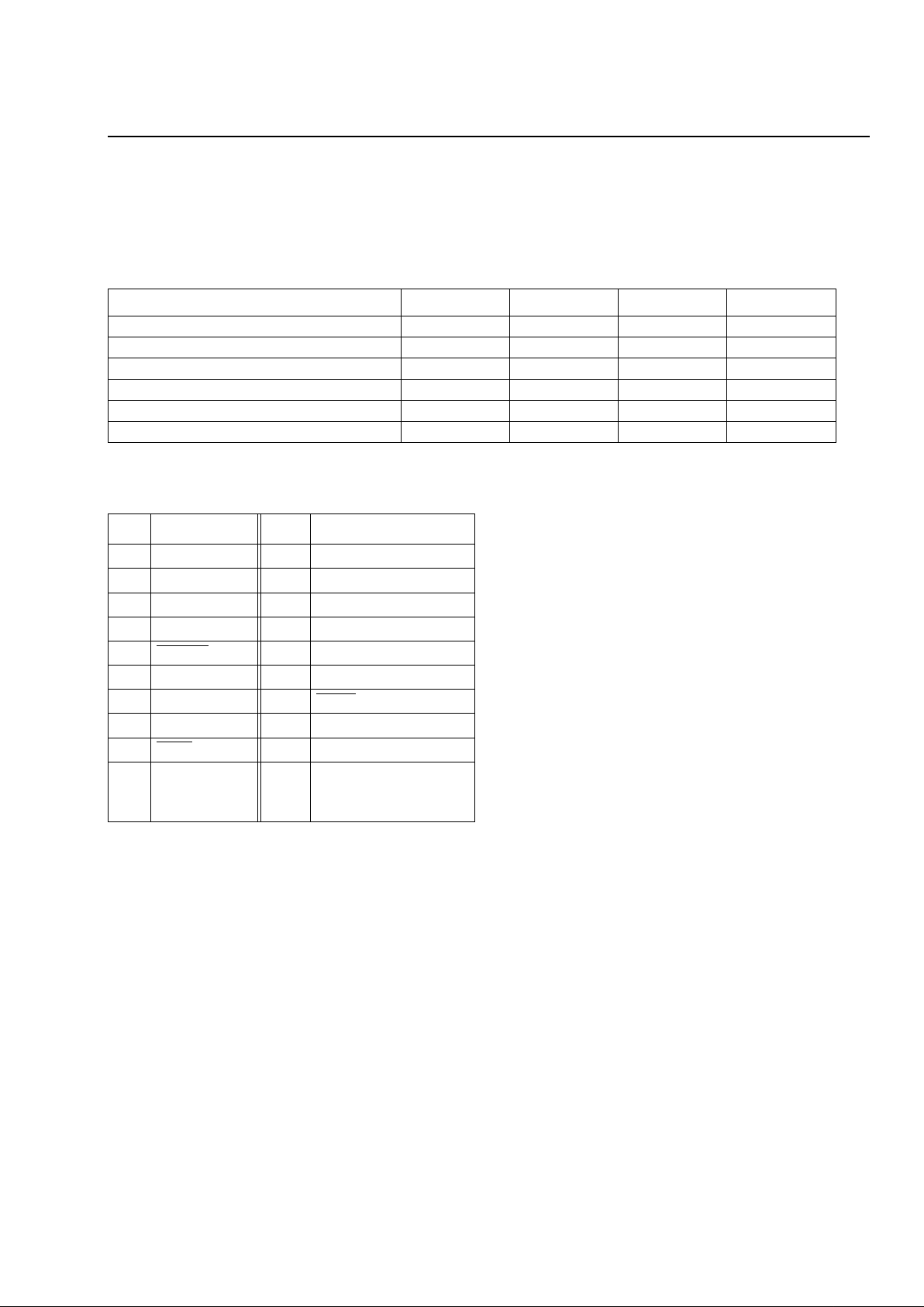
Absolute Maximum Ratings
Stresses in excess of the absolute maximum ratings can cause permanent damage to the device. These are absolute stress ratings only. Functional operation of the device is not implied at these or any other conditions in excess
of those given in the operational sections of the data sheet. Exposure to absolute maximum ratings for extended
periods can adversely affect device reliability.
Parameter Symbol Min Max Unit
Supply Voltage V
CC
05.5V
Operating Case Temperature Range T
C
–40 85 °C
Storage Case Temperature Range T
stg
–40 85 °C
Lead Soldering Temperature/Time — — 250/10 °C/s
Operating Wavelength Range λ 1.1 1.6 µm
Minimum Fiber Bend Radius — 1.0 (25.4) — in. (mm)
Pin Information
* Pins designated as no user connection are not connected inter-
nally. However, to allow for future functional upgrades, it is recommended that the user not make any connections to these pins.
†
The link status flag is a logic flag that indicates the presence or
absence of a minimum acceptable level of optical input. A logic
high on the FLAG output indicates the presence of a valid optical
signal.
Mounting and Connections
The pigtail consists of a 39 in. ± 4 in. (1 m ± 10 cm),
62.5 µm core/125 µm cladding multimode fiber. The
standard fiber has a 0.036 in. (914 µm) diameter tightbuffered outer-jacket. The minimum fiber bending
radius during operation is 1.0 in. (25.4 mm).
Electrostatic Discharge
CAUTION: This device is susceptible to damage
as a result of electrostatic discharge
(ESD). Take proper precautions during
both handling and testing. Follow guidelines such as
EIA
®
Standard
EIA
-625.
Although protection circuitry is designed into the
device, take proper precautions to avoid exposure to
ESD.
Agere Systems Inc. employs a human-body model
(HBM) for ESD susceptibility testing and protectiondesign evaluation. ESD voltage thresholds are dependent on the critical parameters used to define the
model. A standard HBM (resistance = 1.5 kΩ capacitance = 100 pF) is widely used and, therefore, can be
used for comparison purposes. The HBM ESD threshold established for the 1345 receiver is ±1000 V.
Receiver Processing
The 1345-Type receiver devices can withstand normal
wave-soldering processes. The complete receiver
module is not hermetically sealed; therefore, it should
not be immersed in or sprayed with any cleaning solution or solvents. The process cap and fiber pigtail jacket
can deform at temperatures greater than 85 °C. The
receiver pins can be wave-soldered at maximum temperature of 250 °C for 10 seconds.
Pin Name Pin Name
1 Ground 20 No User Connection*
2 Ground 19 No User Connection*
3 Ground 18 No User Connection*
4 CLOCK 17 No User Connection*
5CLOCK
16 Ground
6 Ground 15 Ground
7DATA 14FLAG
†
8 Ground 13 Ground
9DATA
12 FLAG
†
10 No Internal
Connection or
Optional V
PIN
11 V
CC

4
4
Agere Systems Inc.
1345-Type Receiver with Data Sheet
Clock Recovery and Data Retiming January 2000
Application Information
The 1345 receiver is a highly sensitive fiber-optic
receiver. Although the data outputs are digital logic levels (PECL), the device should be thought of as an analog component. When laying out the printed-wiring
board (PWB), the 1345 receiver should be given the
same type of consideration one would give to a sensitive analog component.
At a minimum, a double-sided printed-wiring board with
a large component-side ground plane beneath the
receiver must be used. In applications that include
many other high-speed devices, a multilayer PWB is
highly recommended. This permits the placement of
power and ground connections on separate layers,
which helps minimize the coupling of unwanted signal
noise into the power supplies of the receiver.
Layout Considerations
A fiber-optic receiver employs a very high-gain, widebandwidth transimpedance amplifier. The amplifier
detects and amplifies signals that are only tens of nA in
amplitude. Any unwanted signal currents that couple
into the receiver circuitry cause a decrease in the
receiver's sensitivity and can also degrade the performance of the receiver's loss of signal (FLAG) circuit. To
minimize the coupling of unwanted noise into the
receiver, route high-level, high-speed signals such as
transmitter inputs and clock lines as far away as possible from the receiver pins. If this is not possible, then
the PWB layout engineer should consider interleaving
the receiver signal and flag traces with ground traces in
order to provide the required isolation.
Noise that couples into the receiver through the power
supply pins can also degrade device performance. The
application schematics, Figures 2—3, show recommended power supply filtering that helps minimize
noise coupling into the receiver. The bypass capacitors
should be high-quality ceramic devices rated for RF
applications. They should be surface-mount components placed as close as possible to the receiver power
supply pins. The ferrite bead should have as high an
impedance as possible in the frequency range that is
most likely to cause problems. This will vary for each
application and is dependent on the signaling frequencies present on the application circuit card. Surfacemount, high-impedance beads are available from several manufacturers.
Data and Flag Outputs
The data and clock outputs of the 1345 receiver are
driven by open-emitter NPN transistors which have an
output impedance of approximately 7 Ω. Each output
can provide approximately 50 mA maximum output current. Due to the high switching speeds of ECL outputs,
transmission line design must be used to interconnect
components. To ensure optimum signal fidelity, both
data outputs (DATA and DATA
) and clock outputs
(CLOCK and CLOCK
) should be terminated identically.
The signal lines connecting the data and clock outputs
to the next device should be equal in length and should
have matched impedances.
Controlled impedance stripline or microstrip construction must be used in order not to degrade the quality of
the signal into the next component and to minimize
reflections back into the receiver. Excessive ringing due
to reflections caused by improperly terminated signal
lines makes it difficult for the component receiving
these signals to decipher the proper logic levels and
may cause transitions to occur where none were
intended. Also, by minimizing high frequency ringing
due to reflections caused by improperly designed and
terminated signal lines, possible EMI problems can be
avoided. The applications sections in the Signetics™
ECL 10K/100K Data Manual
or the National Semicon-
ductor
®
ECL Logic Databook and Design Guide
pro-
vide excellent design information on ECL interfacing.
The FLAG and FLAG
outputs of the OC-3/STM-1
155 Mbits/s receiver and the OC-12/STM-4 622 Mbits/s
receiver are 5 V TTL logic-level compatible. The FLAG
output is provided directly by the comparator IC. However, the FLAG output is derived from the FLAG
output
through an inverter. Excessive loading of the FLAG
out-
put can cause the FLAG output to malfunction.
Recommended User Interface
The 1345 receiver is designed to be operated from a
5 V power supply and provides raised or pseudo-ECL
(PECL) data outputs. Figures 2 and 3 show two possible application circuits for the 1345 receiver. Figure 2
represents an application for a PECL compatible interface while Figure 3 shows a possible application for an
ac-coupled, ECL-compatible interface. In both
instances, the DATA outputs are terminated with a
Thévenin equivalent circuit, which provides the equivalent of a 50 Ω load terminated to (V
CC
– 2 V). A single
50 Ω resistor terminated to (V
CC
– 2 V) could also be
used, but this requires a second power supply. Other
methods of terminating ECL-type outputs are discussed in the references previously mentioned.
 Loading...