

AGERE 1340TMPC, 1340TBPC, 1340TAPC, 1340FNPC, 1340FMPC Datasheet
...
Data Sheet
January 2000
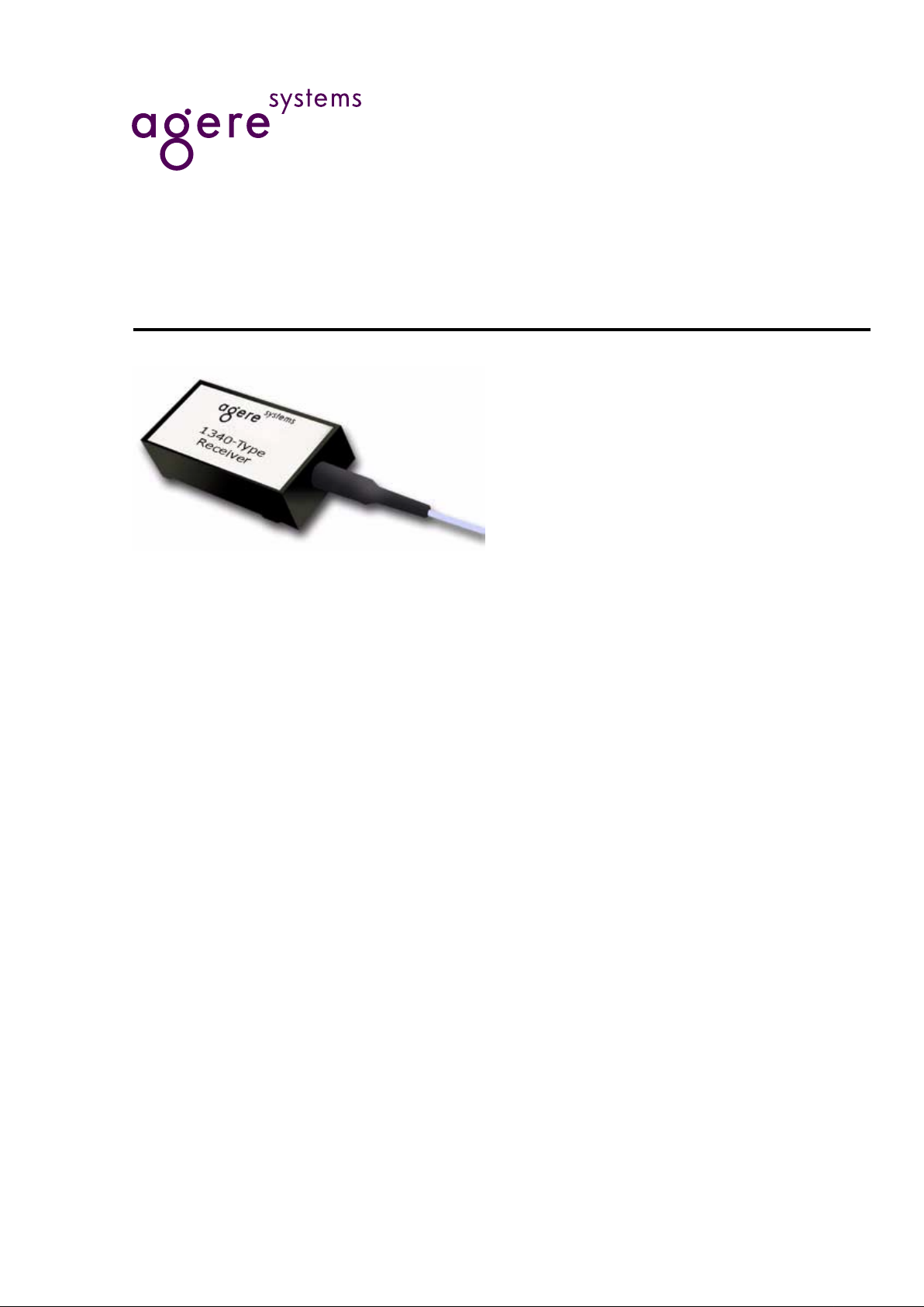
1340-Type Lightwave Receiver
Operating at 1.1 µm through 1.6 µm wavelengths and at
155 Mbits/s, 622 Mbits/s, or 1. 2 5 G bit s /s , the versatile
1340-Type Rec eiv er is man ufactured in a 20-pin, plastic D IP
with a multimode fiber pigtail.
Features
■
Backward compatible with 1310 receiver family
■
Space-saving, self-contained, 20-pin plastic DIP
■
Silicon-based ICs
■
Single 5 V power supply operation including photocurrent monitor capability
■
Exceeds all SONET (GR-253-CORE) and ITU-T
G.958 jitter requirements
■
Wide dynamic range
■
Qualified to meet the intent of Telcordia Technologies
* reliability practices
■
Operates at data rates of 155 Mbits/s,
622 Mbits/s, or 1.25 Gbits/s
■
Positive ECL (PECL) data outputs
■
CMOS (TTL) link-status flag output
■
Operation at 1.3 µm or 1.55 µm wavelengths
■
Operating case temperature range of
–40 °C to +85 °C
Applications
■
Telecommunications:
—Inter- and intraoffice SONET/ITU-T SDH
—Subscriber loop
—Metropolitan area networks
■
High-speed data communications
Description
The 1340-Type receiver is designed for use in transmission systems or medium- to high- speed data
communications applications at data rates up to
1.25 Gbits/s. Compact packaging, along with wide
dynamic range, makes these receivers ideal for both
telecommunications and data communications applications.
The following three versions of the receiver are available:
■
SONET/SDH compliant with OC-3/STM-1
■
SONET/SDH compliant with OC-12/STM-4
■
1.25 Gbits for data applications.
* Telcordia Technologies is a trademark of Telcordia Technologies,
Inc.
22 Agere Systems Inc.
Data Sheet
January 2000
1340-Type Lightwave Receiver
Description
(continued)
The SONET/SDH versions of the receiver are fully
compliant with the latest issue of Telcordia Tec hnolo-
gies GR-253- CORE and the most recent issues of ITU
recommendations G.957 and G.958. The 1340-Type
receiver requires only a single 5 V power supply for
operation. All versions of the receiver are characterized
for operation ove r the case operating range of –40 °C
to +85 °C at the appropriate data rate for each version.
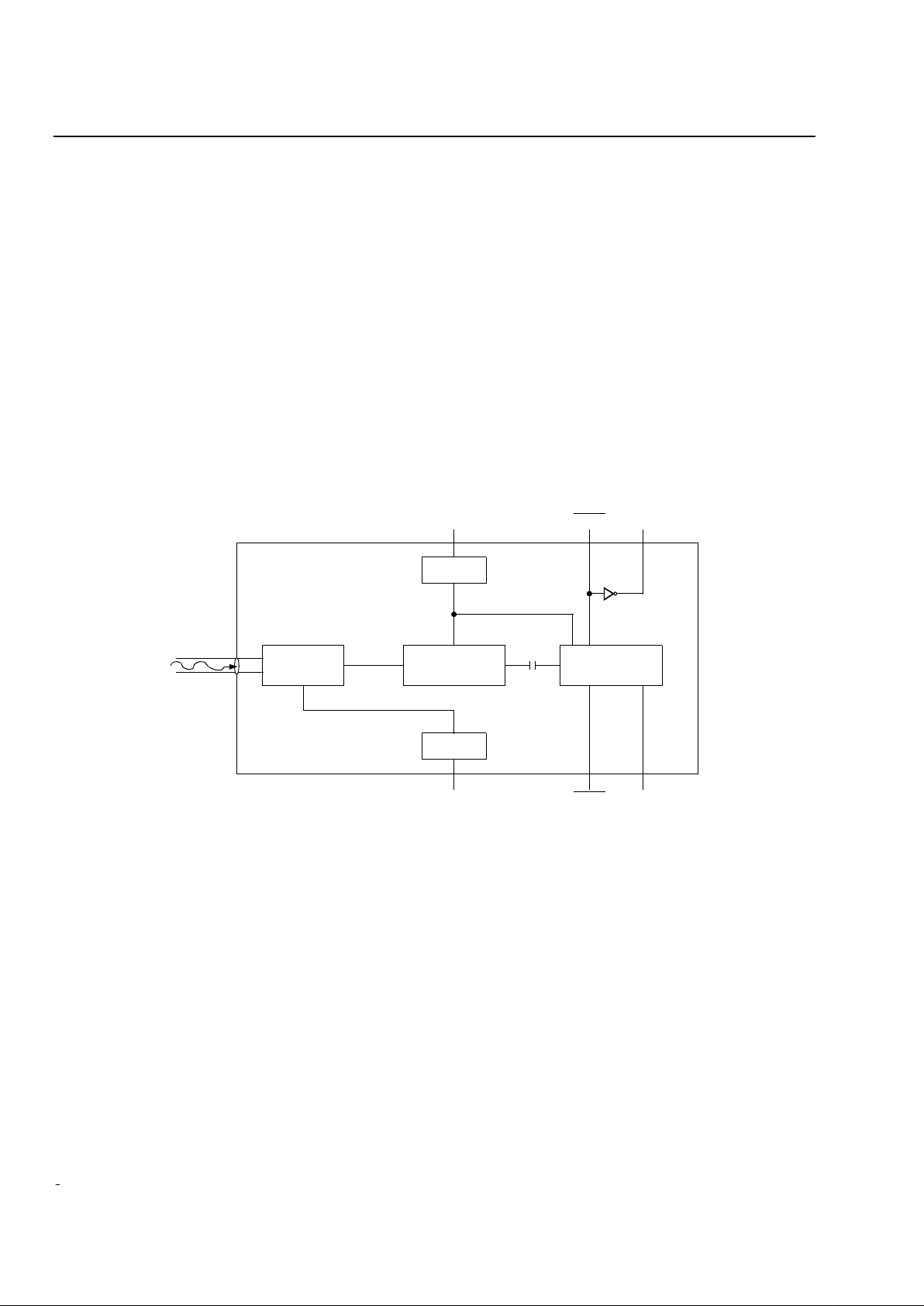
Manufactured in a 20-pin DIP, the receivers use a planar, rea r illuminated InGaAs P IN photode tector that
allows these receivers to be used at wavelengths from
1.1 µm to 1.6 µm. The photocurrent output of the PIN
detector is amplified and converted to a voltage by a
silicon amplifi er. A silic on quantizer provides additional
signal amplification, data threshold detection, and
PECL data outputs. The incoming optical signal is coupled into the receiver through a 62.5 µm core multimode fiber pigtail. The outer j acket diameter of the
pigtail is 900 µm. The receiver can be ordered with the
pigtail terminated in a n FC/PC, SC, or ST
®
optical connector. Other connectors are a vailab le on special order .
See your Agere account representative for ordering
conditions and inform ation.
The receiver has differential PECL data outputs and,
depending on the version selected, either differential
PECL link status flag or complementary CMOS link
status flag outputs. The link status flag outputs indicate
the presence or absence of a minimum acceptable
level of optical input signal.
1-414(F)
Figure 1. Block Diagram
GaAs
PREAMPLIFIER
FILTER
InGaAs
PIN
Si
COMPARATOR
DATA
DATA
FLAG
FLAGV
CC
V
PIN
FILTER

Data Sheet
January 2000
1340-Type Lightwave Receiver
Agere Systems Inc. 3
Description
(continued)
To help ensure high product reliability and custom er
satisfaction, Agere is committed to an intensive quality
program that star ts in the design phase and proceeds
through the manufacturing and shipping process. Optoelectronics subsystems are qualified to Agere internal
standards using MI L-ST D-883 te st methods and procedures and sampling techniques consistent with Tel-
cordia Technologies requirements. The 1340 receiver
qualification program meets the intent of Telcordia
Technologies TR-NWT-000468 and TA-TSY-000983.
Application Information
The 1340 receive r i s a highly sensitive fiber-optic
receiver. Although the data outputs are digital logic levels (PECL), the device should be thought of as an analog component. When laying out the printed-wiring
board (PWB), the 1340 receiver should be given the
same type of consideration one would give to a sensitive analog component.
At a minimum, a double-sided printed-wiring board with
a large component-side ground plane beneath the
receive r must be used. In appli cations tha t incl ude
many other high-speed devices, a multilayer PWB is
highly recommended. T his permits the placement of
power and ground connections on separate layers,
which helps minimize the coupling of unwanted signal
noise into the power supplies of the receiver.
Layout Considerations
A fiber-optic receiver employs a very high-gain, widebandwidth transimpedance amplifier. The amplifier
detects and amplifies signals that are only tens of nA in
amplitude. Any unwanted signal currents that couple
into the receiver circuitry cause a decrease in the
receiver’s sensitivity and can also degrade the performance of the receiver’s loss of signal (FLAG) circuit.
To minimize the coupling of unwanted noise into the
receiver, route high-level, high-speed signals such as
transmitter inputs and clock lines as far away as possible from the receiver pins. If this is n ot po ssible, then
the PWB layout engineer should consider interleaving
the receiver signal and flag traces with ground traces in
order to provide the required isolation.
Noise that couples into the receiver through the power
supply pins can also degrade device performance. The
application schematics, F igures 3—5, show recommended power supply filtering that helps minimize
noise coupling into the receiver. The bypass capacitors
should be high-quality ceramic devices rated for RF
applications. They should be surface-mount components placed as close as possible to the receiver power
supply pins. The ferrite bead should have as high an
impedance as p ossible in the frequency range that is
most likely to cause problems. This will vary for each
application and is dependent on the signaling frequencies present on the application circuit card. Surfacemount, high-impedance beads are available from several manufacturers.
Data and Flag Outputs
The data outputs of the 1340 receiver are driven by
open-emitter NPN transistors which have an output
impedance of approximately 7 Ω. Each output can provide approximately 50 m A maximum output current.
Due to the high switching speeds of ECL outputs,
transmission line design must be us ed to interconnect
components. To ensure o ptimum signal fidelity, both
data outputs (DATA and DATA
) should be terminated
identically . The signal lines connecting the data outputs
to the next device should be equal in length and should
have matched impedances.
Controlled impedance stripline or microstrip construction must be used to preserve the quality of the signal
into the next component and to minimize reflections
back into the receiver. Excessive ringing due to reflections caused by improperly terminated signal lines
makes it difficult for the component receiving these signals to decipher the pr oper logic levels and may cause
transitions to occur where none were intended. Also , by
minimizing high frequency ringing due to reflections
caused by improperly designed and terminated signal
lines, possible EMI problems can be avoided. The
applications sections in the Signetics
*
ECL 10K/100K
Data Manual or the National Semiconductor
†
ECL
Logic Databook and Design Guide provide excellent
design information on ECL interfacing.
* Signetics is a registered trademark of Signetics Corp.
† National Semiconductor is a registered trademark of National
Semiconductor Corporation.
44 Agere Systems Inc.
Data Sheet
January 2000
1340-Type Lightwave Receiver
Data and Flag Outputs
(continued)
The FLAG and FLAG
outputs of the OC-3/STM-1
155 Mbits/s version of the 1340 receiver are PECL
logic levels dr iven by open emitter transistors wi th the
same characteristics as the data outputs. These outputs must be properly terminated in order to obtain the
correct logic levels. Since the FLAG function is basically a dc switch that indicates the loss of optical input
signal, it can be interfaced to much slower TTL or
CMOS logic circuits.
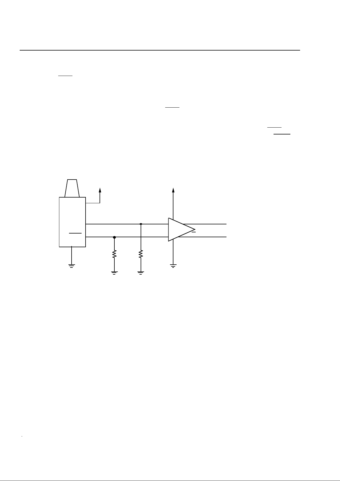
The circuit shown in Figure 2 provides one example of
how to create a TTL logic output from the PECL FLAG
output signal. The outputs of the LT1016 are TTL-compatible and provide both true and inverted logic levels.
The Q output of this circuit will be a TTL high (>2.5 V)
when the 1340 is receiving an optical signal gr e at er
than the FLAG switching threshold and will be a TTL
low (<0.4 V) whenever the optical s ignal is absent or is
below the FLAG switching threshold. The FLAG and
FLAG
outputs of the OC-12/STM- 4 and 1.25 Gbits/s
receivers are 5 V TTL logic level compatible. The FLAG
output is provided directly by the comparator IC. However, the FLAG output is derived from the FLAG
output
through an inverter. Excessive loading of the FLAG
out-
put can cause the FLAG output to malfunction.
1-800(C).a
* Part available from Linear Technology Corporation of Milpitas, CA 95035.
Figure 2. Converting PECL FLAG Outputs to TTL
11
12
14
10 k•
TTL (TRUE)
TTL (INVERTED)
LT1016*
1340
RX
FLAG
FLAG
+5 V +5 V
10 k•
+
–
Q
Q
 Loading...