

AGERE 1245FBDC, 1245FAFC, 1245CBDC, 1245CAFC, 1243FBDC Datasheet
...
Data Sheet
September 1999
1241/1243/1245-Type Uncooled Laser Transmitter
Offering multiple output p ower o ptio ns an d SONE T/SDH compatib ility, the 12 41 / 1 243-Type Uncooled Laser Transmi tt er is
manufactured in a 20-pin, plastic DIP with a single-mode fiber
pigtail.
Features
■
Backward compatible with 1227/1229/1238-Type
Laser Transmitters
■
Space-saving, self-contained, 20-pin DIP
■
Uses field-proven, reliable InGaAsP MQW laser
■
Requires single 5 V power supply
■
SONE T /SDH c ompat ible
■
Uncooled laser with automatic optical power control for constant output power over case temperature range
■
No thermoel ec tric cooler required; reduces size
and power consumption
■
Uses low-power dissipation CMOS technology
■
Qualified to meet the intent of Bellcore reliability
practices
■
Operates over data rates to 1062.5 Mbits/s (NRZ)
■
Operation at 1.3 µm or 1.55 µm wavelength
■
Typical average output power options of –11 dBm,
–8 dBm, –5 dBm, –2 dBm, and 0 dBm
■
ECL compatible, differential inputs
■
Operating temperature range of –40 °C to +85 °C
■
Transmitter-disable option
Applications
■
Telecommunications
— Inter- and intraoffice SONET/ITU-T SDH
— Subscriber loop
— Metropolitan area networks
■
High-speed data communications
— Fibre channel (FC-0)

2 Agere Systems Inc.
Data Sheet
1241/1243/1245-Type Uncooled Laser Transmitter September 1999
Description
The 1241/1243/1245-type Laser Transmitters are
designed for use in transmission systems and highspeed data communication applications. Used in
intraoffice and inter mediate-reach applications, the
transmitters are configured to operate at SONET rates
up to OC-12, as well as at ITU-T synchronous digital
hierarchy (SDH) rates up to STM-4. Specific versions
are also capable of operating up to 1062.5 Mbits/s.
The transmitter meets all present Bellcore GR-253CORE requirements, ANSI T1.117-1991 SONET single-mode, and the ITU-T G.957 and G.958 recommendations. (See Table 5 to select transmitters for the
various SONET/SDH segments.)
The transmitter requires a single power supply (+5 V or
–5 V) and operates over data rates of 1 Mbits/s to
622 Mbits/s (NRZ). Automatic power control circuitry
provides constant optical output power over the operating case temperature range. The automatic power control circuitry also compensates for laser aging. The
optical wavelength tolerance at 25 °C is 1310 nm. The
temperature coefficient of wavelength for 1.3 µm FabryPerot transmitters (1241-Type) is ap proximately
0.4 nm/°C. The temperature coefficient of wavelength
for 1.3 µm and 1.55 µm distributed-feedback (DFB)
transmitters (1243/1245-Type) is approximately
0.1 nm/°C.
Transmitters are available for operation over several dif-
ferent temperature ranges from –40 °C to +85 °C. Manufactured in a 20-pin DIP, the transmitter consists of a
hermetic, InGaAs laser and a single CMOS driver IC.
The low-power consumption circuit provides modulation, automatic optical output power control, and data
reference. The module can be driven by either ac- or
dc-coupled data in single-ended or differential configuration. (See Recommended User I nte rfaces section for
typical connection schemes.) The laser bias and backfacet monitor currents are electrically accessible for
transmitter performance monitoring. The transmitter
optical output may be disabled by a logic-level input.
Functional Overview
Transmitter Circuit Description and
Operation
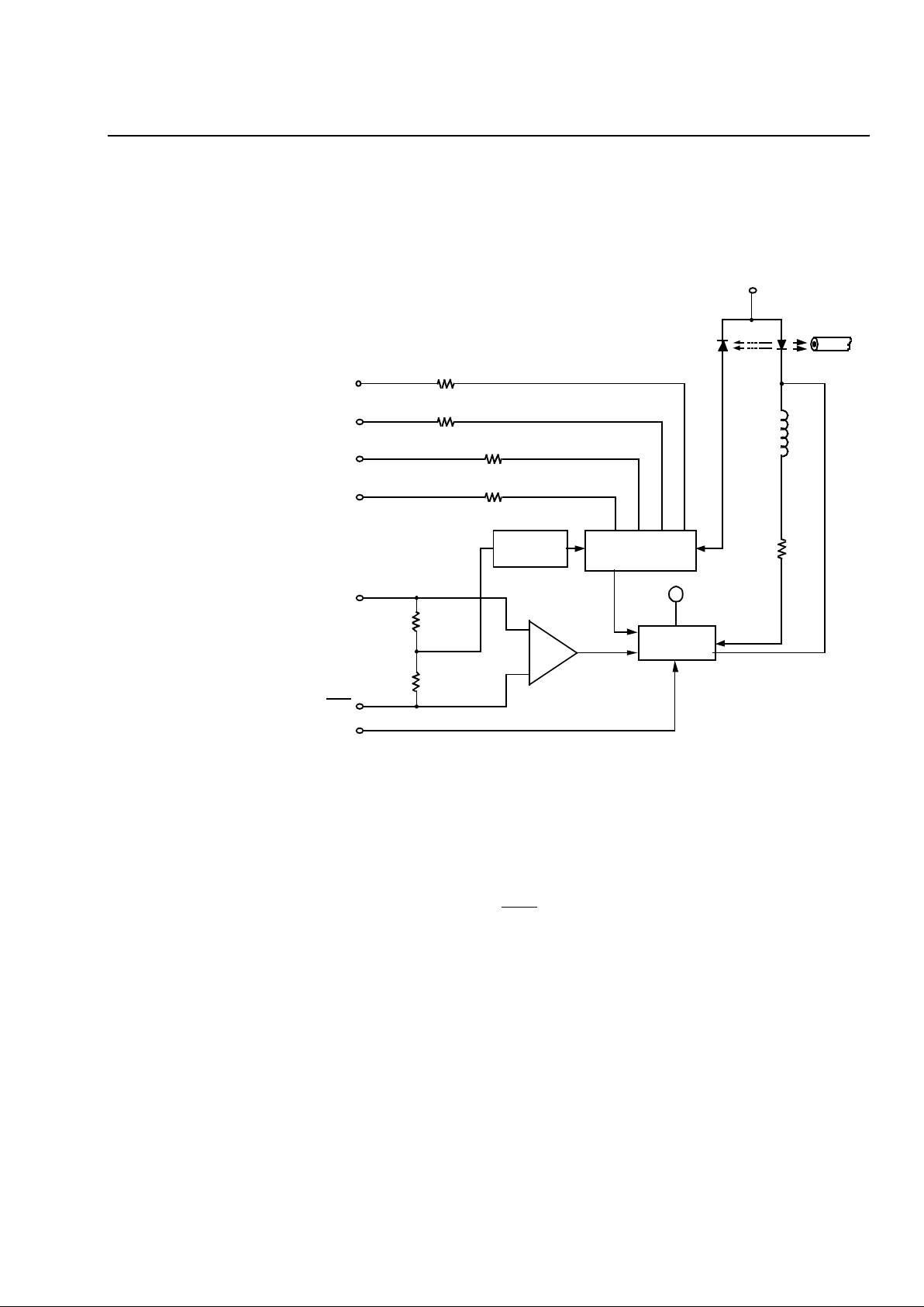
Figure 1 shows a simplified schematic of the transmitter; pin information is listed in Table 1. The laser within
the transmitter is driven by a single CMOS integrated
circuit, which provides the input data signal re ference
level with automatic, temperature-compensated laser
bias, and modulation-current control. A back-facet pho-
todetector diode within the laser module provides an
indication of the laser's average optical output power.
The back-facet diode current is accessible as a voltage
proportional to photocurrent through pins 17 and 19 on
the transmitter. The back-facet diode also forms part of
the feedback control circuit, which helps maintain constant output power.
The laser bias current is accessible as a dc-voltage by
measuring the voltage developed across pins 2 and 4
of the transmitter. Dividing this voltage by 10 Ω will
yield the value o f the laser bias curr e n t. T his value will
change up o r down in re sponse to operating temperature, power supply voltage, data pattern, and laser
aging characteristics.
Table 1. Pin Descriptions
* Pins d esignate d as no user co nnection sh ould not be tied to
ground or any other circuit potential.
† Lase r back-facet and bi as m on itor funct io ns a re cu stomer-us e
optio ns that are not require d for normal operations of the transmitter. They are normally used during manufacture a nd f or
diagnostics.
Pin Number Name
1 No user connection
*
2 Laser bias monitor (+)
†
3 No user connection
*
4 Laser bias monitor (–)
†
5V
EE
6V
CC
7 Transmitter disable
8V
CC
9V
CC
10 No user connection
†
11 Case ground (RF ground)
12 V
CC
13 Case ground (RF ground)
14 V
EE
15 DATA
16 DATA
17 Laser back-facet monitor (–)
*
18 V
CC
19 Laser back-facet monitor (+)
*
20 No user connection
†
Data Sheet
September 1999
Agere Systems Inc. 3
1241/1243/1245-Type Uncooled Laser
Functional Overview
(continued)
1-868(C).h
Figure 1. Simplified Transmitter Schematic Input Data
LASER BACK-FACET MONITOR VOLTAGE
15 k•
(2)
(4)
(+)
(–)
15 k•
LASER BIAS MONITOR VOLTAGE
15 k•
(19)
(17)
(+)
(–)
15 k•
BAND GAP
REFERENCE
AUTOMATIC POWER
CONTROL CIRCUITRY
INPUT DATA
COMPARATOR
MODULATION
CIRCUITRY
TEMPERATURE
SENSOR
t
I
BF
I
BIAS
V
CC
LASER
BACK-FACET
DETECTOR
FIBER PIGTAIL
10 •
DATA
(16)
(7)
(15)
TRANSMITTER
DISABLE
V
CC
– 1.3 V
30 k•
30 k•
DATA
I
MOD
Input Data
Data enter s the transmitt er through a comparator.
These inputs have internal pull-down resistors to a voltage reference that is 1.3 V below V
CC
. Thi s conf i guration allows the transmitter to be driven from either a
single-ended or a differential input signal. Since the
input is a comparator instead of a gate, the absolute
input signal levels are not important when the inputs
are driven differentially. When driven single-ended,
however, the input signal voltage should be centered
around V
CC
– 1.3 V to eliminate pulse-width distortion.
With a single-ended input, either input can be used and
the unused input can be left as an open circu i t due to
the internal reference shown in Figure 1. The optical
output signal will be in the same sense as the input
data—an input logic high turns the laser diode on and
an input logic low turns the laser diode off. However, if
the nega tive input is used with a single-ended data
input signal, the optical signal will be the complement
of the data input signal.
The differental inputs of the 1241 Gbit versions are terminated internally with 100 Ω between t he DATA and
DA TA
inputs.
Minimum Data Rate
Because the modulation and bi as control circuitry are
influenced by the input data pattern, the standard
transmitter cannot be used in burst-mode type applications. For burst-mode applications, please contact your
Agere Account Man ager. The minimum data rate
(pseudorandom data, 50% average duty cycle) for the
1241/1243/1245-Type Transmitters is approximately
1 Mbit/s.

4 Agere Systems Inc.
Data Sheet
1241/1243/1245-Type Uncooled Laser Transmitter September 1999
Functional Overview
(continued)
Since most applications operate at very high data
rates, high-frequency design techni ques need to be
used to ensure optimum performance from the transmitter and interfacing circuitry. Input signal paths
should be kept as short and as straight as possible; differential signal lines should be equal in length, and
controlled-impedance stripline or microstrip construction should always be used when laying out the printedwiring board traces for the data lines. The Recommended User Inter faces section of this data sheet
shows several methods of interfacing to the transmitter.
Power Supplies
The transmitter is configured for operation from either a
single +5 V power supply or a single –5 V power supply . F or positive power supply operation, connect Vcc to
the +5 V power supply and connect V
EE
to ground or
circuit common. For operation from a –5 V power supply, connect V
CC
to ground and connect VEE to the –5 V
power supply. Whichever option is chosen, the V
CC
or
V
EE
connection to the transmitter should be well filtered
to prevent power supply noise from interfering with
transmitter operation.
Transmitter Specifications
Optical Output Power
During manufacture, the optical output power of every
transmitter is tuned to the typical value specified in the
data sheet for that particular transmitter code. The tuning is performed at room ambient and a power supply
voltage of 5 V. The minimum and maximum values
listed in the data sheet for each code group reflect the
worst-case limits that the transmitter is expected to
operate within over its lifetime and over the allowed
power supply and the operating temperature range.
Every transmitter shipped receives a final test, which
includes a SONET eye-mask test at either the OC-3
(STM-1) data rate of 155.52 Mbits/s, the OC-12 (STM4)
data rate of 622.08 Mbits/s, or the fibre channel FC-0
data rate of 1062.5 Mbits/s. The eye-mask test is
meant to examine the performance of the transmitter's
output optical waveform relative to a minimum data pattern eye opening.
Connector Opti ons
The standard optical fiber pigtail is 8 µm core singlemode fiber having a 0.036 in. (914 µm) diameter tightbuffered outer-jacket. The standard length is 39 in. ±
4 in. (1 m ± 10 cm) and c an be te rm inated w ith either
an SC or FC-PC optical connector. Other connector
options may be available on special order . Contact your
Agere Account Manager for ordering information.
Handling Precautions
CAUTION: This device is susceptible to damage as
a result of electrostatic discharge (ESD).
Take proper precautions during both
handling and testing. Follow guidelines
such as JEDEC Publication No. 108-A
(Dec. 1988).
Although protection circuitry is designed into the
device, take proper precautions to avoid exposure to
ESD. Agere employs a human-body model (HBM) for
ESD-suscepti bility testing and protection -design evaluation. ESD voltage thresholds are dependent on the
critical parameters used to define the model. A stan dard HBM (resistance = 1.5 kΩ, capacitance = 100 pF)
is wi dely used and, there fore, can be used for comparison purposes. The HBM ESD withstand voltage established for the 1241-/1243- T yp e Transmitter is ±1000 V.
Transmitter Processing
The transmitter can withstand normal wave-soldering
processes. The complete transmitter module is not hermetically sealed; therefore, it should not be immersed
in or sprayed with any cleaning solut io n or solvents.
The process cap and fiber pigtail jacket deformation
temperature is 85 °C. Transmitter pins can be wavesoldered at maximum temperature of 250 °C for
10 seconds.
Installation Considerations
Although the transmitter features a robust design, care
should be used during handling. Th e optical connector
should be kept free from dust, and the process ca p
should be kept in place as a dust cover when the
device is not connected to a cable. If contamination is
present on the optical connector, canned air with an
exten sion tube can be used to remove any debris.
Other cleaning procedures are identified in the technical note, Cleaning Fiber-Optic As se mblies (TN95010LWP).
 Loading...