

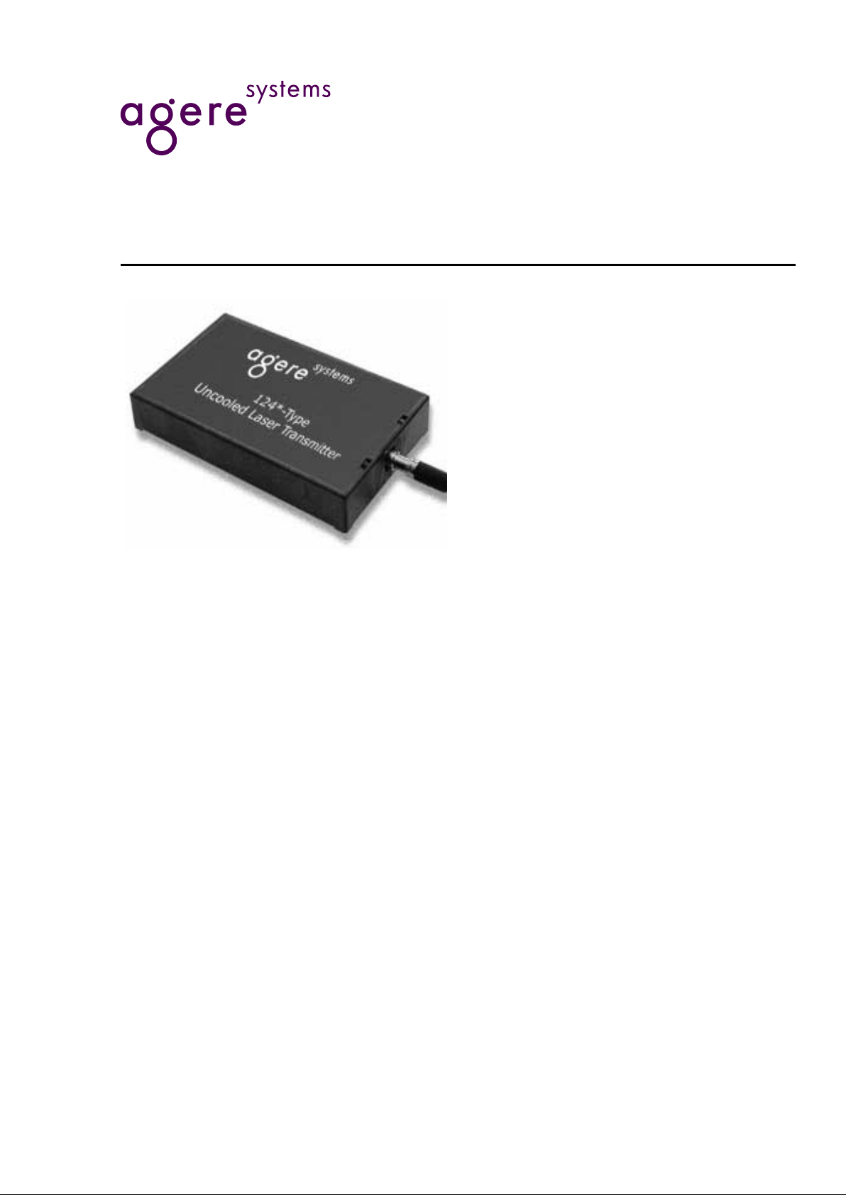
Data Sheet
September 1999
1241/1243/1245-Type Uncooled Laser Transmitter
Offering multiple output p ower o ptio ns an d SONE T/SDH compatib ility, the 12 41 / 1 243-Type Uncooled Laser Transmi tt er is
manufactured in a 20-pin, plastic DIP with a single-mode fiber
pigtail.
Features
■
Backward compatible with 1227/1229/1238-Type
Laser Transmitters
■
Space-saving, self-contained, 20-pin DIP
■
Uses field-proven, reliable InGaAsP MQW laser
■
Requires single 5 V power supply
■
SONE T /SDH c ompat ible
■
Uncooled laser with automatic optical power control for constant output power over case temperature range
■
No thermoel ec tric cooler required; reduces size
and power consumption
■
Uses low-power dissipation CMOS technology
■
Qualified to meet the intent of Bellcore reliability
practices
■
Operates over data rates to 1062.5 Mbits/s (NRZ)
■
Operation at 1.3 µm or 1.55 µm wavelength
■
Typical average output power options of –11 dBm,
–8 dBm, –5 dBm, –2 dBm, and 0 dBm
■
ECL compatible, differential inputs
■
Operating temperature range of –40 °C to +85 °C
■
Transmitter-disable option
Applications
■
Telecommunications
— Inter- and intraoffice SONET/ITU-T SDH
— Subscriber loop
— Metropolitan area networks
■
High-speed data communications
— Fibre channel (FC-0)

2 Agere Systems Inc.
Data Sheet
1241/1243/1245-Type Uncooled Laser Transmitter September 1999
Description
The 1241/1243/1245-type Laser Transmitters are
designed for use in transmission systems and highspeed data communication applications. Used in
intraoffice and inter mediate-reach applications, the
transmitters are configured to operate at SONET rates
up to OC-12, as well as at ITU-T synchronous digital
hierarchy (SDH) rates up to STM-4. Specific versions
are also capable of operating up to 1062.5 Mbits/s.
The transmitter meets all present Bellcore GR-253CORE requirements, ANSI T1.117-1991 SONET single-mode, and the ITU-T G.957 and G.958 recommendations. (See Table 5 to select transmitters for the
various SONET/SDH segments.)
The transmitter requires a single power supply (+5 V or
–5 V) and operates over data rates of 1 Mbits/s to
622 Mbits/s (NRZ). Automatic power control circuitry
provides constant optical output power over the operating case temperature range. The automatic power control circuitry also compensates for laser aging. The
optical wavelength tolerance at 25 °C is 1310 nm. The
temperature coefficient of wavelength for 1.3 µm FabryPerot transmitters (1241-Type) is ap proximately
0.4 nm/°C. The temperature coefficient of wavelength
for 1.3 µm and 1.55 µm distributed-feedback (DFB)
transmitters (1243/1245-Type) is approximately
0.1 nm/°C.
Transmitters are available for operation over several dif-
ferent temperature ranges from –40 °C to +85 °C. Manufactured in a 20-pin DIP, the transmitter consists of a
hermetic, InGaAs laser and a single CMOS driver IC.
The low-power consumption circuit provides modulation, automatic optical output power control, and data
reference. The module can be driven by either ac- or
dc-coupled data in single-ended or differential configuration. (See Recommended User I nte rfaces section for
typical connection schemes.) The laser bias and backfacet monitor currents are electrically accessible for
transmitter performance monitoring. The transmitter
optical output may be disabled by a logic-level input.
Functional Overview
Transmitter Circuit Description and
Operation
Figure 1 shows a simplified schematic of the transmitter; pin information is listed in Table 1. The laser within
the transmitter is driven by a single CMOS integrated
circuit, which provides the input data signal re ference
level with automatic, temperature-compensated laser
bias, and modulation-current control. A back-facet pho-
todetector diode within the laser module provides an
indication of the laser's average optical output power.
The back-facet diode current is accessible as a voltage
proportional to photocurrent through pins 17 and 19 on
the transmitter. The back-facet diode also forms part of
the feedback control circuit, which helps maintain constant output power.
The laser bias current is accessible as a dc-voltage by
measuring the voltage developed across pins 2 and 4
of the transmitter. Dividing this voltage by 10 Ω will
yield the value o f the laser bias curr e n t. T his value will
change up o r down in re sponse to operating temperature, power supply voltage, data pattern, and laser
aging characteristics.
Table 1. Pin Descriptions
* Pins d esignate d as no user co nnection sh ould not be tied to
ground or any other circuit potential.
† Lase r back-facet and bi as m on itor funct io ns a re cu stomer-us e
optio ns that are not require d for normal operations of the transmitter. They are normally used during manufacture a nd f or
diagnostics.
Pin Number Name
1 No user connection
*
2 Laser bias monitor (+)
†
3 No user connection
*
4 Laser bias monitor (–)
†
5V
EE
6V
CC
7 Transmitter disable
8V
CC
9V
CC
10 No user connection
†
11 Case ground (RF ground)
12 V
CC
13 Case ground (RF ground)
14 V
EE
15 DATA
16 DATA
17 Laser back-facet monitor (–)
*
18 V
CC
19 Laser back-facet monitor (+)
*
20 No user connection
†
Data Sheet
September 1999
Agere Systems Inc. 3
1241/1243/1245-Type Uncooled Laser
Functional Overview
(continued)
1-868(C).h
Figure 1. Simplified Transmitter Schematic Input Data
LASER BACK-FACET MONITOR VOLTAGE
15 k•
(2)
(4)
(+)
(–)
15 k•
LASER BIAS MONITOR VOLTAGE
15 k•
(19)
(17)
(+)
(–)
15 k•
BAND GAP
REFERENCE
AUTOMATIC POWER
CONTROL CIRCUITRY
INPUT DATA
COMPARATOR
MODULATION
CIRCUITRY
TEMPERATURE
SENSOR
t
I
BF
I
BIAS
V
CC
LASER
BACK-FACET
DETECTOR
FIBER PIGTAIL
10 •
DATA
(16)
(7)
(15)
TRANSMITTER
DISABLE
V
CC
– 1.3 V
30 k•
30 k•
DATA
I
MOD
Input Data
Data enter s the transmitt er through a comparator.
These inputs have internal pull-down resistors to a voltage reference that is 1.3 V below V
CC
. Thi s conf i guration allows the transmitter to be driven from either a
single-ended or a differential input signal. Since the
input is a comparator instead of a gate, the absolute
input signal levels are not important when the inputs
are driven differentially. When driven single-ended,
however, the input signal voltage should be centered
around V
CC
– 1.3 V to eliminate pulse-width distortion.
With a single-ended input, either input can be used and
the unused input can be left as an open circu i t due to
the internal reference shown in Figure 1. The optical
output signal will be in the same sense as the input
data—an input logic high turns the laser diode on and
an input logic low turns the laser diode off. However, if
the nega tive input is used with a single-ended data
input signal, the optical signal will be the complement
of the data input signal.
The differental inputs of the 1241 Gbit versions are terminated internally with 100 Ω between t he DATA and
DA TA
inputs.
Minimum Data Rate
Because the modulation and bi as control circuitry are
influenced by the input data pattern, the standard
transmitter cannot be used in burst-mode type applications. For burst-mode applications, please contact your
Agere Account Man ager. The minimum data rate
(pseudorandom data, 50% average duty cycle) for the
1241/1243/1245-Type Transmitters is approximately
1 Mbit/s.

4 Agere Systems Inc.
Data Sheet
1241/1243/1245-Type Uncooled Laser Transmitter September 1999
Functional Overview
(continued)
Since most applications operate at very high data
rates, high-frequency design techni ques need to be
used to ensure optimum performance from the transmitter and interfacing circuitry. Input signal paths
should be kept as short and as straight as possible; differential signal lines should be equal in length, and
controlled-impedance stripline or microstrip construction should always be used when laying out the printedwiring board traces for the data lines. The Recommended User Inter faces section of this data sheet
shows several methods of interfacing to the transmitter.
Power Supplies
The transmitter is configured for operation from either a
single +5 V power supply or a single –5 V power supply . F or positive power supply operation, connect Vcc to
the +5 V power supply and connect V
EE
to ground or
circuit common. For operation from a –5 V power supply, connect V
CC
to ground and connect VEE to the –5 V
power supply. Whichever option is chosen, the V
CC
or
V
EE
connection to the transmitter should be well filtered
to prevent power supply noise from interfering with
transmitter operation.
Transmitter Specifications
Optical Output Power
During manufacture, the optical output power of every
transmitter is tuned to the typical value specified in the
data sheet for that particular transmitter code. The tuning is performed at room ambient and a power supply
voltage of 5 V. The minimum and maximum values
listed in the data sheet for each code group reflect the
worst-case limits that the transmitter is expected to
operate within over its lifetime and over the allowed
power supply and the operating temperature range.
Every transmitter shipped receives a final test, which
includes a SONET eye-mask test at either the OC-3
(STM-1) data rate of 155.52 Mbits/s, the OC-12 (STM4)
data rate of 622.08 Mbits/s, or the fibre channel FC-0
data rate of 1062.5 Mbits/s. The eye-mask test is
meant to examine the performance of the transmitter's
output optical waveform relative to a minimum data pattern eye opening.
Connector Opti ons
The standard optical fiber pigtail is 8 µm core singlemode fiber having a 0.036 in. (914 µm) diameter tightbuffered outer-jacket. The standard length is 39 in. ±
4 in. (1 m ± 10 cm) and c an be te rm inated w ith either
an SC or FC-PC optical connector. Other connector
options may be available on special order . Contact your
Agere Account Manager for ordering information.
Handling Precautions
CAUTION: This device is susceptible to damage as
a result of electrostatic discharge (ESD).
Take proper precautions during both
handling and testing. Follow guidelines
such as JEDEC Publication No. 108-A
(Dec. 1988).
Although protection circuitry is designed into the
device, take proper precautions to avoid exposure to
ESD. Agere employs a human-body model (HBM) for
ESD-suscepti bility testing and protection -design evaluation. ESD voltage thresholds are dependent on the
critical parameters used to define the model. A stan dard HBM (resistance = 1.5 kΩ, capacitance = 100 pF)
is wi dely used and, there fore, can be used for comparison purposes. The HBM ESD withstand voltage established for the 1241-/1243- T yp e Transmitter is ±1000 V.
Transmitter Processing
The transmitter can withstand normal wave-soldering
processes. The complete transmitter module is not hermetically sealed; therefore, it should not be immersed
in or sprayed with any cleaning solut io n or solvents.
The process cap and fiber pigtail jacket deformation
temperature is 85 °C. Transmitter pins can be wavesoldered at maximum temperature of 250 °C for
10 seconds.
Installation Considerations
Although the transmitter features a robust design, care
should be used during handling. Th e optical connector
should be kept free from dust, and the process ca p
should be kept in place as a dust cover when the
device is not connected to a cable. If contamination is
present on the optical connector, canned air with an
exten sion tube can be used to remove any debris.
Other cleaning procedures are identified in the technical note, Cleaning Fiber-Optic As se mblies (TN95010LWP).

Agere Systems Inc. 5
Data Sheet
September 1999
1241/1243/1245-Type Uncooled Laser
Absolute Maximum Ratings
Stresses in excess of the absolute maximum ratings can cause permanent damage to the device. These are absolute stress ratin gs onl y. Functional operation o f the device is not implied at thes e or any other conditions in excess
of those given in the operations sections of the data sheet. Exposure to absolute maximum ratings for extended
periods can adversely affect device reliability.
*With VEE connected to –5 V, VCC must be at 0 V; with VCC connected to +5 V, V
EE
must be at 0 V.
†
Specification depends upon the code ordered. The de vice is capable of a cold start at –40 °C; specifications are me t
after a warm-up t ime determined by the system thermal design.
Characteristics
Minimum and maximum values specified over operating case temperature range at 50% duty cycle data signal and
end of life (EOL). Typical values ar e measured at beginning-of-life (BOL) room temperature unless otherwise noted.
Table 2. Electrical Characteristics
1. With V
EE
connected to –5 V, VCC must be at 0 V; with VCC connecte d to +5 V, V
EE
must be at 0 V.
2. Input measured from V
CC
with 50 Ω load to (VCC – 2 V). 10K, 10K H, an d 100K ECL compatible.
3. Between 10% and 90% (50% duty cycle) where t is the bit period in ns.
4. The tr ansmitter is normally enabled and only requires a n external vo ltage to disable.
5. Time measured from rising edge of disable signal until optical output (laser diode) has turned off.
6. Time measured from falling edge of enable signal until optical output has stabilized at nominal output power level.
7. The laser bias current is obtained by dividing the bias voltage by the 10 Ω current -sensing r esistors. (See Figure 1.) When measuri ng these
voltage s or using them in conjunction w ith alarm circuits, use a high-inpu t impedance device.
8. The la ser back-facet monitor volt age is a scaled output that tracks the transmitter optical output power.
Parameter Symbol Min Max Unit
Supply Voltage
*
——5.5V
Operating Case Temperature Range
†
T
C
–40 85 °C
Storage Case Temperature Range T
stg
–40 85 °C
Lead Soldering Temperature/Time — — 250/10 °C/s
Relative Humidity (noncondens ing) RH — 85 %
Minimum Fiber Bend Radi us — 1.00 (25.4) — in. (mm)
Parameter Symbol Min Typ Max Unit
Power Supply Voltage
1
V 4.75 5.0 5.50 V
Power Supply Current Drain I
TOTAL
— 30 130 mA
Input Data Voltage:
2
Low
High
VIL
V
IH
–1.81
–1.16
—
—
–1.47
–0.88
V
V
Input Transition Time
3
t
I
—t/4—ns
Transmitter Disable Voltage
4
V
D
VCC – 2.0 — V
CC
V
Transmitter Enable Voltage V
EN
V
EE
—VEE + 0.8 V
Output Disable Time
5
t
D
— — 0.20 µs
Output Enable Time
6
t
EN
— — 2.00 µs
Laser Bias Voltage
7
V
B
0.01 0. 06 0.70 V
Laser M on it o r Voltage (50% duty cycl e )
8
V
BF
0.01 0. 05 0.20 V

66 Agere Systems Inc.
Data Sheet
September 1999
1241/1243/12 45-Ty pe Unco ole d Las er Transmitter
Characteristics
(continued)
Table 3. Optic al Characteristics
1. Output power definitions and measurement per ITU-T Recommenda tion G.957 and G.958.
2. Ratio of logic 1 to logic 0 power levels.
3. Be t ween 10% and 90 % ( 50 % duty cycle).
4. Roo t- m ean-squa r e spectra l wi dth accoun ts for modes up to and inclu ding thos e 20 dB down from the central mode.
(Applies to 1241-Type only. )
5. Ap pl ie s to 1243/124 5-Type only.
Recommended User Interfaces
1-496(C).c
* Locate th ese compo ne nt s a s cl os e to DATA/DATA inputs as possible.
Note: The 1241 gigab it version does not require the externa l 50 Ω terminations since this termi nation is included inside the module.
Figure 2. dc-Coupled, Differential Input
Parameter Symbol Min Typ Max Unit
Average Power Output Options
1
P
O
See Ordering Information. dBm
Extinctio n Ratio
2
r
E
10 — — dB
Optical Rise and Fall Times
3
:
OC-3/STM-1
OC-12/STM4
1062.5 Mbits/s
t
R
, t
F
tR, t
F
tR, t
F
—
—
—
—
—
—
1.0
0.5
0.37
ns
ns
ns
Center Wavelength λ See Ordering Information. nm
RMS Spectral Width
4
∆λ ——4nm
Side-mode Suppression Ratio
5
SMSR 30 — — dB
ECL
DRIVER
D
TRANSMITTER
15
16
50 •*
360 •
360 •
V
EE
D
V
EE
50 •*
0.1 µF
50 • MICROSTRIP OR STRIPLINECONTROLLED IMPEDANCE TRACES
Agere Systems Inc. 7
Data Sheet
September 1999
1241/1243/1245-Type Uncooled Laser
Recommended User Interfaces
(continued)
1-497(C)
Note: Input ca n als o be c on ne c ted to DATA; unused i nput pin remains unconnected.
(622 M bits/s and below only.)
Figure 3. dc-coupled, Single-Ended Input
1-498(C)
* This network introduces a slight offset between DATA and DATA, which tur ns the laser
transmitter off wh en there is no data present at the inputs. ( 622 Mbits/ s and below only.)
Figure 4. ac-Coupled, Single-Ended Input
Qualification and Reliability
To help ensure high product reliability and customer satisfaction, Agere Systems is committed to an intensive quality program that starts in the design phase and proceeds through the manufacturing proc ess. Optoelectronics modules are qualified to Agere Systems internal standards using MIL-STD-883 test methods and procedures and using
sampling techniques consistent with Bellcore requirements. The 1241/1243/1245 series of transmitters have
undergone an extensive and rigorous set of qualification tests. This qualification program fully meets the intent of
Bellcore reliability practices TR-NWT-000468 and TA-NWT-00 0983. In addition, the design, development, and manufacturing facility of the Optoelectronics unit at Agere Systems has been certified to be in full compliance with the
latest ISO-9001 Quality System Standards.
50 •
15
16
1.0 µF
VCC – 2 V
(CUSTOMER
SUPPLIED)
50 • COAX
OR 50 •
STRIPLINE
D
TRANSMITTER
D
50 •
15
16
50 • COAX
OR 50 •
STRIPLINE
1.0 µF
1.0 µF
619 •
27 •
1960 •
V
EE
V
CC
D
TRANSMITTER
D
*
*
*
88 Agere Systems Inc.
Data Sheet
September 1999
1241/1243/12 45-Type Uncooled Las er Transmitter
Outline Diagram
Dimensions are in inches and (millimeters). Unless otherwise noted, toleranc es are ±0.005 in (±0.127 mm).
1-987C).a
1.339
(34.01)
0.950
(24.13)
0.635
(16.14)
0.144
(3.66)
TOP VIEW
PIN 1 INDICATOR
0.125
(3.18)
0.110
(2.80)
0.100
(2.54)
0.900
(22.86)
0.350 (8.89)
0.400
(10.16)
PIN 20PIN 11
PIN 1PIN 10
BOTTOM VIEW
0.018
(0.46)

Agere Systems Inc. 9
Data Sheet
September 1999
1241/1243/1245-Type Uncooled Laser
Laser Safety Information
Class I Las e r Produ ct
All versions of the 1241/1243/1245-Type transmitters are Class I laser products per CDRH, 21 CFR 1040 Laser
Safety requirements. The 1241/1243/1245-Type transmitters have been classified with the FDA under accession
number 8720009. All versions are Class I laser products per IEC 825-1:1993.
CAUTION: Use of controls, adjustments, and procedures other than those specified herein may result in
hazardous laser radiation exp osure.
This product complies with 21 CFR 1040.10 and 1040.11.
8.8 µm single-mode pigtail with connector
Wavelength = 1.3 µm
Maximum power = 1.6 mW
Notice
Unterminated optical connectors may emit laser radiation.
Do not view with optical instruments.
Table 4. A gere Trans m itters for SONET/SDH Applications
* Full SONE T/ S DH co mp liance, –4 0 °C to +85 °C.
† Full SON ET / SD H co mp li ance, –20 °C t o +70 °C.
Connector
Type
1.3 µm Transmitter Type
*
1.55 µm Transmitter Type
†
Short and Intermed iate Reach
(<2 km and ~15 km)
Long Reach
~40 km
Long Reach
~80 km
OC-3/
STM-1
OC-12/
STM-4
OC-3/
STM-1
OC-12/
STM-4
OC-3/
STM-1
OC-12/
STM-4
FC-PC 1241FAUC 1241FBUC 1243FAFD 1243FBDC 1245FAFC 1245FBDC
SC 1241CAUC 1241CBUC 1243CAFD 1243CBDC 1245CAFC 1245CBDC

1010 Agere Systems Inc.
Data Sheet
September 1999
1241/1243/12 45-Type Uncooled Las er Transmitter
Ordering Information
Table 5. 1241/1243/1245- Type Transmitter Ordering Information
* ∆λ for these codes is 2.5 nm maximum. All other 1241-type codes are 4 nm maximum.
OC-3/STM-1 Transmitter Codes
Operating
Case Temp.
Range (°C)
Average Output
Power
(dBM)
Center
Wavelength
(nm)
Connector 122x
Equivalent
Product
Order
Code
Comcode
Min Max Min Typ Max Min Max
0 65 –3 0 2 1290 1330 FC-PC 1227AE 1241FADC 108123449
0 65 –3 0 2 1290 1330 SC 1227AF 1241CADC 108123480
0 65 –5 –2 0 1280 1335 FC-PC 1227YA 1241FAFC 108123357
0 65 –5 –2 0 1280 1335 SC 1227YB 1241CAFC 108123373
0 65 –8 –5 –2 1260 1360 SC 1227CA 1241CALC 108123324
0 65 –8 –5 –2 1260 1360 FC-PC 1227C 1241FALC 108123563
–20 70 –5 –2 0 1480 1580 SC 1229CB5 1245CAFC 108400409
–20 70 –5 –2 0 1480 1580 FC-PC 1229FB5 1245FAFC 108400417
–40 85 –5 –2 0 1280 1335 SC 1227YD 1243CAFD 108123423
–40 85 –5 –2 0 1280 1335 FC-PC 1227YE 12 43FAFD 108123415
–40 85 –12 –8 –5 1260 1360 SC 1227FB 1241CAPC 108123282
–40 85 –12 –8 –5 1260 1360 FC-PC 1227F 1241FAPC 108123266
–40 85 –15 –11 –8 1260 1360 SC 1227HA 1241CAUC
*
108123209
–40 85 –15 –11 –8 1260 1360 FC-PC 1227H 1241FAUC
*
108123159
OC-12/STM-4 Transmitter Codes
0 65 –3 0 2 1290 1330 FC-PC 1227AK 1241FBDC 108123456
0 65 –3 0 2 1290 1330 SC 1227AN 1241CBDC 108123498
0 65 –8 –5 –2 1260 1360 FC-PC 1227D 1241FBLC 108123316
–20 70 –3 0 2 1480 1580 SC 1229CA5 1245CBDC 108400391
–20 70 –3 0 2 1480 1580 FC-PC 1229FA5 1245FBDC 108400425
–40 85 –3 0 2 1280 1335 FC-PC 1229FA 1243FBDC 108123506
–40 85 –3 0 2 1280 1335 SC 1229CA 1243CBDC 108123522
–40 85 –12 –8 –5 1260 1360 FC-PC 1227G 1241FBPC 108123274
–40 85 –15 –11 –8 1260 1360 FC-PC 1227AC 1241FBUC
*
108123167
–40 85 –15 –11 –8 1274 1356 SC 1227PG 1241CBU
*
108123217
Fibre Channel—1062.5 Mbits/s
10 65 –11 –8 –5 1260 1360 FC-PC 1238A 1241FCPC 108309287
10 65 –11 –8 –5 1260 1360 FC-PC 1238B 1241FCPD 108309295
10 65 –3 0 2 1290 1330 FC-PC 1238C 1241FCDC 108309279
Agere Systems Inc. 11
Data Sheet
September 1999
1241/1243/1245-Type Uncooled Laser
Part Numbering for the 1241/1243/1245-Type Transmitter
1 2 4 X XXX X Field D escription
Laser Type:
1 = 1.3 µm Fabry-Perot laser, 3 = 1.3 µm DFB laser, 5 = 1.55 µm DFB laser
Optical Connector:
C = SC, F = FC/PC
Data Rate:
A = 155 Mbits/s, B = 622 Mbits/s, C = 1062.5 Mbits/s
Typical Power :
D = 0 dBm, F = –2 dBm, L = –5 dBm, P = –8 dBm, U = –11 dBm
Customer Options:
A—F
Ta ble 6. Related Products
Description Device Number Document Number
155 Mbits/s and 622 Mbits/s for SONET/
SDH Applications
1340-Type Pin Receiver DS99-072LWP
155 Mbits/s and 622 Mbits/s Receivers
with Clock and Data Recovery for
SONET/SDH Applications
1345-Type Pin Receiver with Clock and
Data Recovery
DS99-071LWP

Agere Systems Inc. reserves the right to make changes to the product(s) or information contained herein without notice. No liability is assumed as a result of their use or application.
Copyright © 2001 Agere Systems Inc.
All Rights Reserve d
September 1999
DS99-228LWP (Replaces DS99-073LWP)
For additional information, contact your Agere Systems Account Manager or the following:
INTERNET: http://www.agere.com
E-MAIL: docmaster@agere.com
N. AMERICA: Agere Systems Inc ., 555 Uni on Boulevard, Room 30L-15P-BA, A llentown, PA 18109-3286
1-800-372-2447, FAX 610-712-4106 (In CANAD A : 1-800-553-2448, FAX 610-712-4106)
ASIA: Agere Systems Hong Kong Ltd., Suites 3201 & 3210-12, 32/F, Tower 2, The Gateway, Harbour City, Kowloon
Tel. (852) 3129-2000, FAX (852) 3129-2020
CHINA: (86) 21-5047-1212 (Shanghai), (86) 10-6522-5566 (Beijing), (86) 755-695-7224 (Shenzhen)
JAPAN: (81) 3-5421-1600 (Tokyo), KOREA: (82) 2-767-1850 (Seoul), SINGAPORE: (65) 778-8833, TAIWAN: (886) 2-2725-5858 (Taipei)
EUROPE: Tel. (44) 7000 624624, FAX (44) 1344 488 045
 Loading...