

Page 1
1
1. Product introduction
1.1 Product overview
Category
Item
Parameter
Wireless standards
Wireless parameters
frequency range
2.4GHz
Transmitting power
Receiving sensitivity
Min. -92.5dBm
Antenna type
Onboard antenna
Hardware
parameters
Data interface
UART
Operating Volt
3.3V
Supplying current
≥50mA
Low power consumption
≤6uA
Transmission distance
Outdoor space 80m
Operating Temperature
-40℃ ~ +85℃
Size
23.3x12x2.0mm
CSR1010 Series Smart Bluetooth Modules are designed based on CSR1010 chip, compatible with
Bluetooth 4.1 and low power consumption. (BLE) and Bluetooth module of mesh networking
function. It is mainly used in intelligent lighting control, home/hotel automation control,
Consumer electronics, industrial control, etc. can meet the requirements of low power
consumption, low delay, short-range wireless data communication.
1.2 Product characteristics
* Maximum Receiving Sensitivity: >-92.5dBm
* Maximum transmit power < 7.5dBm
* Voltage input range: 1.9V~3.6V
* The working temperature of the module used in intelligent lighting: - 40℃ ~85 ℃
* Power consumption: sleep mode is as low as 6uA
* Support BLE mesh, compliant with Bluetooth 4.1 specification
* Various peripheral device interfaces
Maximum 5-way PWM output
A UART External Communication Interface
Maximum four-way switching input and relay control output
Max. 11 customized GPIOs
* Support Point-to-Point and Point-to-Multipoint Communication
1.3 Product parameters:
Bluetooth 4.1(BLE mode only)
<7.5dBm
Page 2
2
2. Introduction of Hardware
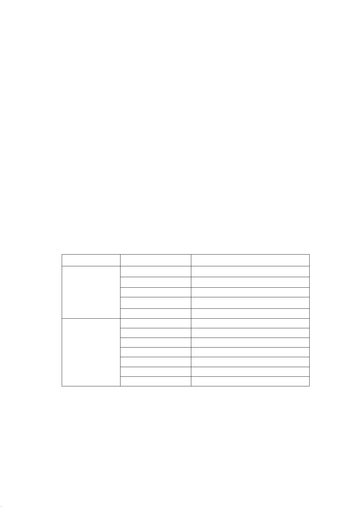
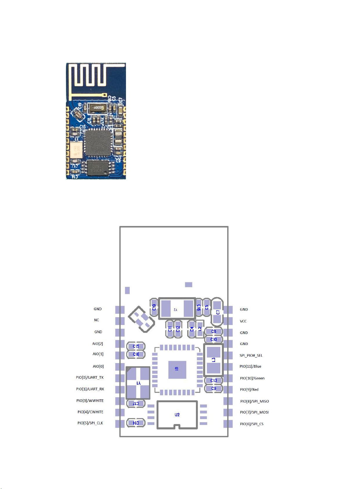
2.1 Module Shape and Interface
2.2 Pin description
The shape of the module is as above, 22 pins are external, and the detailed pin function is
referred to the following table.
Page 3

3
PIN
PIN Function
Description
1
GND
Earth input
2NCNC
3
GND
Earth input
4
AIO[2]
Simulated IO pins can be customized.
5
AIO[1]
Simulated IO pins can be customized.
6
AIO[0]
Simulated IO pins can be customized.
7
PIO[0]/UART_TX
System debugging serial port can be customized to GPIO
function.
8
PIO[1]/UART_RX
System debugging serial port can be customized to GPIO
function.
9
WWHITE
Warm white PWM output, high efficiency; 1KHz frequency.
Customizable to GPIO functionality.
10
CWHITE
Cool white PWM output, high efficiency; 1KHz frequency.
Customizable to GPIO functionality.
11
PIO[5]/SPI_CLK
System debugging port can be customized to GPIO function.
12
PIO[6]/SPI_CS
System debugging port can be customized to GPIO function.
13
PIO[7]/SPI_MOSI
System debugging port can be customized to GPIO function.
14
PIO[8]/SPI_MISO
System debugging port can be customized to GPIO function.
15
PIO[9]/RED
Red PWM output, 3.8KHz frequency, high efficiency; available
in two street lamp firmware. Used as cold white PWM.
Customizable to GPIO functionality.
16
PIO[10]/Green
Green PWM output, 3.8KHz frequency, high efficiency; available
in two street lamp firmware. Used as cold white PWM.
Customizable to GPIO functionality.
17
PIO[11]/Blue
Blue PWM output, high efficiency; can be customized to GPIO
function.
18
SPI_PIO#_SEL
The system reserves debugging pins for SPI mode. Default needs
to be lowered.
19
GND
Earth input
20
GND
Earth input
21
VCC
3.3V DC input
22
GND
Earth input
Note:
1. Pin numbers start from the top left of the module and are arranged counterclockwise.
2. When the module is used for different devices, the function and pin definitions will be
slightly different, referring specifically to the detailed description documents of the
corresponding firmware.
Page 4

FCC Statement
This device complies with part 15 of the FCC Rules. Operation is subject to the following two conditions: (1) This device may not cause harmful
interference, and (2) this device must accept any interference received, including interference that may cause undesired operation.
Changes or modifications not expressly approved by the party responsible for compliance could void the user's authority to operate the
equipment.
NOTE: This equipment has been tested and found to comply with the limits for a Class B digital device, pursuant to Part 15 of the FCC Rules.
These limits are designed to provide reasonable protection against harmful interference in a residential installation. This equipment generates,
uses and can radiate radio frequency energy and, if not installed and used in accordance with the instructions, may cause harmful interference
to radio communications. However, there is no guarantee that interference will not occur in a particular installation. If this equipment does
cause harmful interference to radio or television reception, which can be determined by turning the equipment off and on, the user is
encouraged to try to correct the interference by one or more of the following
measures:
-- Reorient or relocate the receiving antenna.
-- Increase the separation between the equipment and receiver.
-- Connect the equipment into an outlet on a circuit different from that to which the receiver is connected.
-- Consult the dealer or an experienced radio/TV technician for help.
FCC Radiation Exposure Statement
This modular complies with FCC RF radiation exposure limits set forth for an uncontrolled environment. This transmitter must not be co-
located or operating in conjunction with any other antenna or transmitter.
If the FCC identification number is not visible when the module is installed inside another device, then the outside of the device into which
the module is installed must also display a label referring to the enclosed module. This exterior label can use wording such as the
following: “Contains Transmitter Module FCC ID: 2AR7I-CSR1010 Or Contains FCC ID: 2AR7I-CSR1010”
when the module is installed inside another device, the user manual of this device must contain below warning statements;
1. This device complies with Part 15 of the FCC Rules. Operation is subject to the following two conditions:
(1) This device may not cause harmful interference.
(2) This device must accept any interference received, including interference that may cause undesired operation.
2. Changes or modifications not expressly approved by the party responsible for compliance could void the user's authority to operate the
equipment.
The devices must be installed and used in strict accordance with the manufacturer's instructions as described in the user documentation
that comes with the product .
Any company of the host device which install this modular with limit modular approval should perform the test of radiated emissionand
spurious emission according to FCC part 15C : 15.247 and 15.209 requirement,Only if the test result comply with FCC part 15C : 15.247 and
15.209 requirement,then the host can be sold legally.
Page 5

4
2.3 PCB Package size:
Module size is 23.3*12 mm, pin spacing is 1.27 mm, pin foot width is 0.846mm.
2.4 Suggestions on the Use of Module PCB
* LDO is recommended for DC 3.3V supply, providing at least 50mA drive capability. A
10uF capacitor is recommended at the module power supply entrance.
* In PCB layout planning, BLE modules should be placed away from magnetic field sources
such as transformers and coils.
* The antenna area should be kept clear of the PCB design and cannot be protected by any
enclosure. Antennas must be at least 10mm away from metal or high components.
 Loading...