

Page 1

VIA C3 Low Power Processors Embedded SBC
User’s Manual
Version 1.4
Page 2

© Copyright 2005. All Rights Reserved
Manual edition 1.4, Nov.2005
This document contains proprietary information protected by copyright. All rights
are reserved, no part of this manual may be reproduced, copied, translated or
transmitted in any form or by any means without prior written permission of the
manufacturer.
The content of this manual is intended to be accurate and reliable, the original
manufacturer assumes no responsibility for any inaccuracies that may be contained in
this manual. The original manufacturer reserves the right to make improvements to
the products described in this manual at any time without prior notice.
Trademarks
IBM, EGA, VGA, XT/AT, OS/2 and PS/2 are registered trademarks of International
Business Machine Corporation
Award is a trademark of Award Software International, Inc
RTL is a trademark of Realtek Semi-Conductor Co., Ltd
VIA is a trademark of VIA Technologies, Inc
Winbond is a trademark of Winbond Technology, Inc
CF and CompactFlash are trademark of ScanDisk Corporation
Microsoft, Windows, Windows NT and MS-DOS are either trademarks or registered
trademarks of Microsoft Corporation
All other product names mentioned herein are used for identification purpose only and
may be trademarks and/or registered trademarks of their respective companies
Limitation of Liability
While reasonable efforts have been made to ensure the accuracy of this manual, the
manufacturer and distributor assume no liability resulting from errors or omissions in
this manual, or from the use of the information contained herein.
i
Page 3

Table of Contents
Chapter 1. General Information
1.1 Introduction---------------------------------------------------------------------------------1
1.2 Specification---------------------------------------------------------------------------------1
1.3 AW-E652 Package--------------------------------------------------------------------------3
1.4 Board Layout--------------------------------------------------------------------------------4
1.5 Board Dimension---------------------------------------------------------------------------4
Chapter 2. Connectors Location and Configuration
2.1 Connectors/Jumpers Location and Define--------------------------------------------5
2.2 Onboard Processors-----------------------------------------------------------------------6
2.3 Installing System Memory----------------------------------------------------------------6
2.4 Connector and Jumpers Settings-------------------------------------------------------7
CN1: VGA D-Sub Connector------------------------------------------------------------7
CN2: COM1 D-Sub Connector---------------------------------------------------------8
CN3: PS/2 Mouse/KB Connector-------------------------------------------------------8
CN4: IR Connector------------------------------------------------------------------------9
CN5: LAN RJ-45 Connector------------------------------------------------------------9
CN6: USB Connector--------------------------------------------------------------------10
CN7: Internal Mouse/KB Pin-Header------------------------------------------------10
CN8: LVDS Connector-------------------------------------------------------------------11
CN9: COM2 Pin-Header----------------------------------------------------------------11
CN10: PCI Interface---------------------------------------------------------------------12
CN11: LPT Pin-Header------------------------------------------------------------------13
CN12: PC/104 Connector---------------------------------------------------------------14
CN13: Power Button---------------------------------------------------------------------15
CN14: GPIO Port Connector----------------------------------------------------------15
CN15: IDE Connector-------------------------------------------------------------------16
CN16: LCD Backlight Connector-----------------------------------------------------17
CN17: Floppy Connector---------------------------------------------------------------17
CN18: USB3/4 Pin-Header-------------------------------------------------------------18
CN19: ATX Power Connector---------------------------------------------------------18
CN20: AC97 Connector-----------------------------------------------------------------18
CN21: +5V/+12 Input Connector-----------------------------------------------------19
CN22: COM3/COM4 Pin-Header----------------------------------------------------19
CN23: LCD Display----------------------------------------------------------------------20
JP1: COM1 RI/Voltage Select----------------------------------------------------------21
JP2: COM2 Mode Select----------------------------------------------------------------21
ii
Page 4

JP3: Clear CMOS-----------------------------------------------------------------------22
JP4: Watchdog Output Select--------------------------------------------------------22
JP5: COM2 RI/Voltage Select--------------------------------------------------------22
JP6: COM4 RI/Voltage Select--------------------------------------------------------23
JP7: COM3 RI/Voltage Select--------------------------------------------------------23
JP8: LCD Voltage Select---------------------------------------------------------------24
JP9: COM2 RS485 Wire Select---------------------------------------------------24
Chapter 3. BIOS Setup-----------------------------------------------------------------------25
3.1 Quick Setup--------------------------------------------------------------------------------25
3.2 Entering the CMOS Setup Program--------------------------------------------------26
3.3 Menu Options------------------------------------------------------------------------------27
Standard CMOS Features--------------------------------------------------------------29
Advanced BIOS Features---------------------------------------------------------------31
Advanced Chipset Features-------------------------------------------------------------34
Integrated Peripherals-------------------------------------------------------------------37
Power Management Setup--------------------------------------------------------------41
PNP/PCI Configuration-----------------------------------------------------------------43
PC Health Status--------------------------------------------------------------------------44
Frequency/Voltage Control-------------------------------------------------------------45
Load Fail-Safe Default-------------------------------------------------------------------45
Load Optimized Default-----------------------------------------------------------------46
Set Supervisor & User Password------------------------------------------------------46
Save & Exit Setup-------------------------------------------------------------------------47
Save Without Saving---------------------------------------------------------------------48
Chapter 4. Drivers and Utilities Installation---------------------------------------------49
System Driver Installation------------------------------------------------------------------49
Audio Driver Installation--------------------------------------------------------------------54
VGA Driver Installation---------------------------------------------------------------------56
Ethernet Driver Installation ----------------------------------------------------------------58
Appendix A. Programming the Watchdog Timer--------------------------------------65
Appendix B. Audio Kit-----------------------------------------------------------------------66
Appendix C. Installing PC/104 Module--------------------------------------------------69
Appendix D. Programming the GPIO Port----------------------------------------------69
Appendix E. Interrupt Controller---------------------------------------------------------70
Appendix F. Optional Cable List----------------------------------------------------------73
iii
Page 5

iv
Page 6

1
Chapter 1. General Information
1.1 Introduction
The AW-E652 is a full function of 3.5” Embedded format SBC board use VIA
VT8606 and VT82C686B chipset supports processors VIA Ezra/Eden (EBGA
packaging) processors. The AW-E652 supports CRT and 36-bit TFT panels, Realtek
RTL8139C+ Ethernet chipset with RJ45 jack for 10/100Mbps and AC-97 Audio
Interface.
The onboard features include three RS-232 and one RS-232/422/485 serial ports, one
bi-directional parallel port and onboard SSD interface supports 50-pin CompactFlash
socket for TypeI/II CompactFlash Card. The AW-E652 supports up to 4 USB
included two USB ports and pin-header for USB3/4, 8 Digital Input/8 Output as well
as the Watchdog timer. For the expansion ability, the AW-E652 reserved a PC/104
connector and proprietary PCI connector onboard.
User’s manual
1.2 Specification
CPU
BIOS
Chipset
I/O Chipset
Memory
Enhanced IDE
FDD interface
Parallel port
Serial port
IR interface
VIA Ezra/Eden (EBGA package) processor
Award® 256KB Flash BIOS
VIA VT8606 + VT82C686B
Built-in VT82C686B + Winbond 83977EF
One 144-pin SO-DIMM socket support up to
512Mbytes SDRAM
Support up to two IDE devices (Ultra DMA
33/66/100).
Support 34-pin header up to two floppy disk drives
One bi-directional parallel port. Support
SPP/ECP/EPP
Three RS-232 and one RS-232/422/485 serial ports.
Support one IrDA Tx/Rx header
KB/Mouse connector
USB connectors
Battery
Wa tchdog T imer
Support PC/AT keyboard and PS/2 mouse
Support four USB ports
Lithium battery for data retention up to 10 years(in
normal condition)
Can generate a system reset, or IRQ11. Support
software selectable timeout interval.
AW-E652
Page 7

User’s manual
2
Digital I/O
PCI Connector
PC/104 Connector
Power management
Flat Panel/CRT Interface
Chipset
Display memory
Interface
Display type
Ethernet Interface
Eight digital output and eight input
Optional proprietary PCI connector for PCI
expansion
One PC/104 connector
APM 1.1 compliant
VIA Twister chip with integrated Savage4
2D/3D/V ideo Accelerator
Share system memory 8/16/32MB
4x AGP VGA/LCD interface, support for 9, 12, 15,
18, 24, 36 bit TFT and optional 16 or 24-bit DSTN
Panel
Support CRT, 36bit TTL TFT LCD and LVDS
interface
Chipset
Ethernet interface
SSD Interface
Sound Interface (Optional via Audio Kit)
Chipset
Audio controller
Audio interface
Mechanical and Environmental
Power supply voltage
Max. power requirements
Operating temperature
Board size
Realtek RTL8139C+ 100Base-TX Fast Ethernet
controller
PCI 100/10 Mbps Ethernet controller
One 50-pin CompactFlash™ socket
Option AC 97 codec
SoundBlaster Pro Hardware and Direct Sound
Ready AC97 Digital Audio
Mic in,, Line in, Speaker out and CD audio in
VCC (4.75V to 5.25V)
4A @ 5 V, 200mA/+12V
32 to 140°F (0 to 60°C)
5.7"(L) x 4"(W) (145mm x 102mm)
Weight
1.3 AW-E652 Package
Please make sure that the following items have been included in the
package before installation.
1. AW-E652 VIA C3 Single Board
0.26 lb. (0.57 Kg) (bare)
AW-E652
Page 8

3
2. Quick Setup
3. Cable: Please refer to Appendix F Optional Cables
4. CD-ROM which contains the following fol ders:
(1) Manual
(2) LAN Driver
(3) Tools
(4) Chipset Driver
(5) VGA Driver
(6) Sound Driver
If any of these items are missing or damaged, please contact your dealer
from whom you purchased the board at once. Save the shipping
materials and carton in the event that you want to ship or store the board
in the future. After you unpack the board, inspect it to assure an intact
shipment. Do not apply power to the board if it appears to have been
User’s manual
damaged.
Leave the board in its original packing until you are ready to install
Precautions
Please make sure you properly ground yourself before handling the AW-E652 board
or other system components. Electrostatic discharge can be easily damage the
AW-E652 board.
Do not remove the anti-static packing until you are ready to install the AW-E652
board.
Ground yourself before removing any system component from it protective anti-static
packaging. To ground yourself, grasp the expansion slot covers or other unpainted
parts of the computer chassis.
Handle the AW-E652 board by its edges and avoid touching its component.
1.4 Board Layout
AW-E652
Page 9

1.5 Board Dimension
User’s manual
4
Chapter 2. Connectors/Jumpers Location and Configuration
AW-E652
Page 10

5
User’s manual
2.1 Connectors/Jumpers Location and Define
CN1 CN2 CN3 CN5 CN6
CN4
CN19
CN7
CN9
CN10
CN15
CN13
CN11
CN18
CN17
CN8
CN12
CN14
CN16
JP2
JP5
JP9
CN21
JP1
JP6 JP7
JP3
CN23CN20CN22
JP4
JP8
AW-E652
Page 11

User’s manual
Connector Description Connector Description
CN1 VGA Connector (D-Sub) CN13 Power Button
CN2 COM1 Connector (D-Sub) CN14 GPIO Port Connector
CN3 PS/2 KB/MS Connector (D-Sub) CN15 IDE Connector
CN4 IR Connector CN16 LCD Backlight Enable Connector
CN5 LAN Connector (RJ45) CN17 Floppy Connector
CN6 USB Connector CN18 USB3/4 Connector (Pin Header)
CN7 Internal KB/MS Connector(Hader) CN19 ATX Power Connector
CN8 LVDS Connector CN20 AC97 Connector
CN9 COM2 Connector(RS232/422/485) CN21 +5V/+12V Input Connector
CN10 PCI Interface CN22 COM3/COM4 Connector (Header)
CN11 LPT1 Connector (Pin Header) CN23 LCD Display Connector
CN12 PC/104 Connector
Pin Define Pin Define
JP1 COM1 RI/Voltage Select JP5 COM2 RI/Voltage Select
JP2 COM2 Mode Select JP6 COM4 RI/Voltage Select
JP3 Clear CMOS JP7 COM3 RI/Voltage Select
JP4 Watchdog Output Select JP8 LCD Voltage Select
JP9 COM2 RS485 Wire Select
6
2.2. Onboard Processors
The AW-E652 has onboard built-in VIA Ezra or EDEN EBGA Package processor.
The CPU cooler fan will be mounted when board with 800MHz or 667MHz CPU and
the high profile Heatsink will be mounted when 667MHz CPU.
2.3 Installing Memory
To insert a SO-DIMM Memory:
The AW-E652 supports one 144-pin SO-DIMM sockets, memory up to 512Mbyte.
To Insert a SO-DIMM Memory: Please align the module with the socket key and
press down until the levers at each end of the socket snap close up.
There is only one direction for installing a module in the socket. Do not attempt to
force the module into the socket incorrectly.
To Remove a SO-DIMM Memory: To remove a SO-DIMM, press down on the
levers at both end of the module until the module pops out
There is only one direction for installing a module in the socket. Do not attempt to
force the module into the socket incorrectly.
AW-E652
Page 12
7
2.4 Connector and Jumper Settings
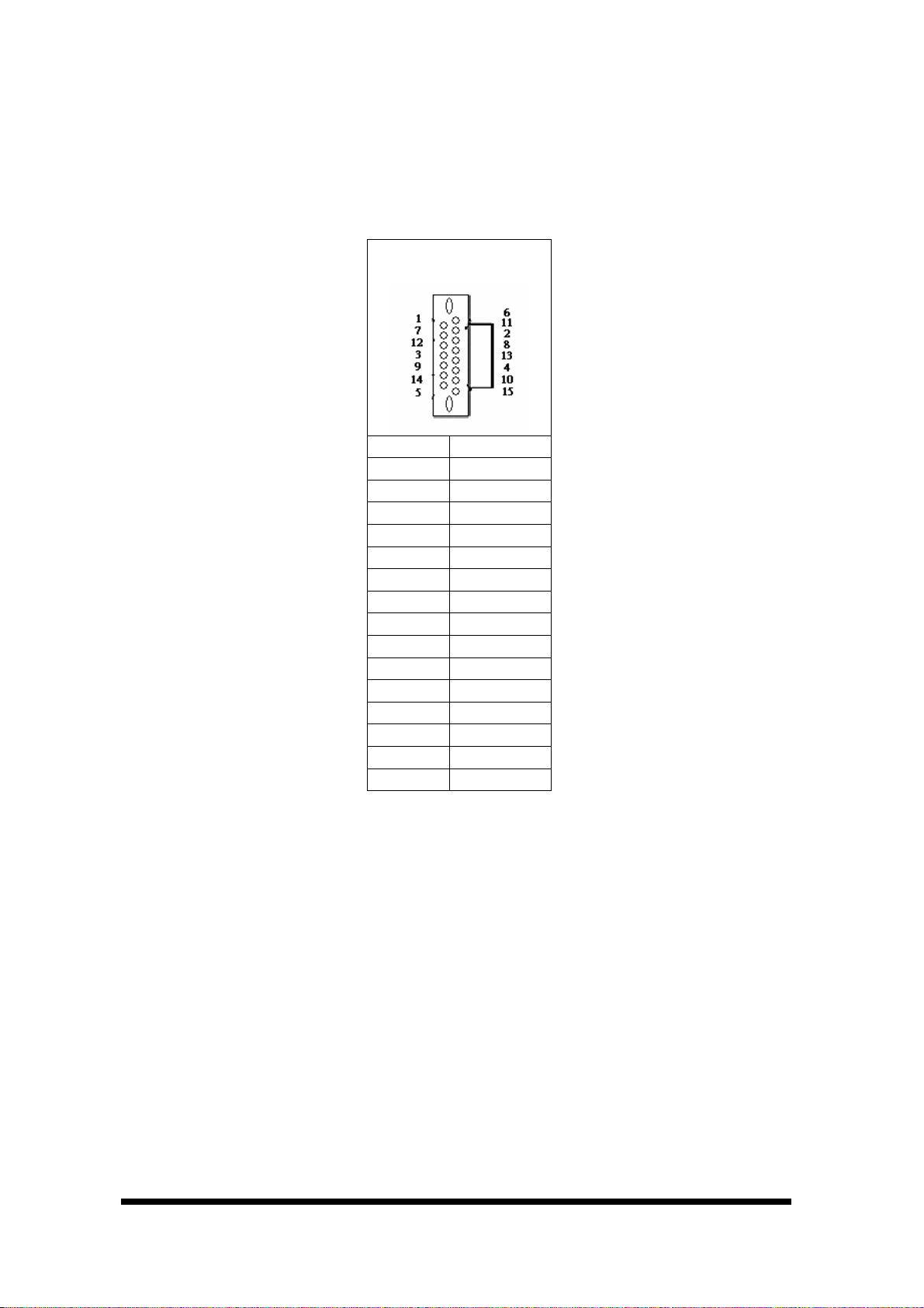
CN1: VGA Connector
User’s manual
Pin Define
1 Red
2 Green
3 Blue
4 MONID0
5 Ground
6 Ground
7 Ground
8 Ground
9 +5V
10 Ground
11 MONID1
12 DDC Data
13 H-Sync
14 V-Sync
15 DDC Clock
AW-E652
Page 13

User’s manual
CN2: COM1 Connector (D-Sub)
Pin Define
1 DCD
2 RXD
3 TXD
4 DTR
5 Ground
6 DSR
7 RTS
8 CTS
9 RI
CN3: PS/2 Mouse/Keyboard Connector (MINI DIN Jack)
8
Pin Define
1 KBDATA
2 MSDATA
3 Ground
4 +5V
5 KBCLK
6 MSCLK
AW-E652
Page 14

9
User’s manual
CN4: IR Connector
The onboard IR connector with a 2.0mm pitch pin header
Pin Define
1 +5V
2 Fast IR Receive
3 IR Receiver
4 Ground
5 IR Transmitter
CN5: LAN Connector (JR-45)
LED:
D1: Speed indicated LED
Pin Define
1 TX0+
2 TX03 RX0+
4 NC
5 NC
6 RX07 NC
8 NC
10 Mbps DIM
100 Mbps GREEN
D2 :Link/Activity LED
Link YELLOW
Activity BLINKING
AW-E652
Page 15

CN6: USB Connector
User’s manual
Pin Define
1 5VUSB0
2 USBDT03 USBDT0+
4 Ground
5 5VUSB0
6 USBDT17 USBDT1+
8 Ground
10
CN7: Internal KB/MS Connec tor
The AW-E652 supports an internal keyboard/mouse with 2mm pitch pin header for
flexible using.
Pin Define
1 KB-CLK
2 KB-DATA
3 MS-CLK
4 Ground
5 KBMSVCC
6 MSDAA
AW-E652
Page 16

11
CN8: LVDS Connector
The AW-E652 supports LVDS by using a 20-pin of connector for LVDS Panel
Pin Define Pin Define
1 Y0P 2 Y1P
3 Y0M 4 Y1M
5 Ground 6 Ground
7 Y2P 8 NC
9 Y2M 10 NC
11 Ground 12 Ground
User’s manual
13 YCP 14 VCCLCD
15 YCM 16 VCC LCD
17 Ground 18 NC
19 V12P0 20 V12P0
CN9: COM2 Connector
The AW-E652 supports four serial ports, onboard COM2 with a 2.00mm pitch pin
header.
Pin Define
1 DCD2#N
2 DSR2#N
3 RXD2 IN
4 RTS#2OUT
5 TXD2OUT
6 CTS2#N
7 DTR#2OUT
8 RI#2_5V_12V
9 Ground
10 NC
11 485TXD+/422TXD+
12 485TXD-/422TXD13 422RXD+
14 422RXD-
AW-E652
Page 17

User’s manual
CN10: PCI Interface
The AW-E652 supports one micro PCI slot for expansion.
Pin Signal Pin Signal Pin Signal Pin Signal
1 GND 26 PCICLK1 51 +3.3V 76 SERR2 GND 27 PCIRST- 52 +3.3V 77 AD15
3 +12V 28 GND 53 AD22 78 C/BE14 +12V 29 GNT4- 54 AD21 79 AD13
12
5 GND 30 +5V 55 AD20 80 AD14
6 +5V 31 REQ2- 56 AD19 81 GND
7 +5V 32 +5V 57 AD18 82 GND
8 +5V 33 +5V 58 AD19 83 AD11
9 +5V 34 REQ4- 59 AD16 84 AD12
10 INTB- 35 +5V 60 C/BE2- 85 AD9
11 INTA- 36 AD31 61 GND 86 AD10
12 INTD- 37 AD30 62 GND 87 C/BE013 INTC- 38 AD29 63 FRAME- 88 AD8
14 REQ3- 39 AD28 64 IRDY- 89 AD6
15 GND 40 +3.3V 65 GND 90 AD7
16 REQ1- 41 GND 66 GND 91 +5V
17 PCICLK2 42 GND 67 TRDY- 92 +5V
18 GNT3- 43 AD26 68 DEVSEL- 93 AD4
19 GND 44 AD27 69 GND 94 AD5
20 GND 45 AD24 70 PLOCK- 95 AD2
21 PCICLK3 46 AD25 71 GND 96 AD3
22 PCICLK0 47 GNT2- 72 GND 97 AD0
23 GND 48 C/BE3- 73 +3.3V 98 AD1
24 GND 49 +3.3V 74 PERR- 99 GND
25 GNT1- 50 AD23 75 PAR 100 GND
AW-E652
Page 18

13
CN11: LPT Connector
The AW-E652 supports a 26-pin pin header LPT connector by using 2mm pitch
connector.
Pin Define Pin Define
1 PT_STB# 14 PTAFD#
2 PT_D0 15 PTERROR#
3 PT_D1 16 PTINT#
4 PT_D2 17 PTSLIN#
5 PT_D3 18 Ground
6 PT_D4 19 Ground
User’s manual
7 PT_D5 20 Ground
8 PT_D6 21 Ground
9 PT_D7 22 Ground
10 PTACK# 23 Ground
11 PTBUSY 24 Ground
12 PTPE 25 Ground
13 PTSLCT 26 Ground
AW-E652
Page 19

User’s manual
CN12: PC/104 Connector
CN12 is a standard PC/104 bus connector, and it is fully occupied with the signals of
the “ISA” (PC/AT) bus. It offers full architecture, hardware and software
compatibility with the ISA bus and can accept ultra-compact (3.6” x 3.8”) stackable
modules.
Signal Pin Signal Pin Signal Pin Signal Pin
Ground C0 Ground D0 IOCHCHK A1 Ground B1
SBHE* C1 MEMCS16* D1 SD7 A2 RESET B2
LA23 C2 IOSC16* D2 SD6 A3 +5V B3
LA22 C3 IRQ10 D3 SD5 A4 IRQ9 B4
LA21 C4 IRQ11 D4 SD4 A5 NC B5
LA20 C5 IRQ12 D5 SD3 A6 NC B6
LA19 C6 IRQ15 D6 SD2 A7 NC B7
LA18 C7 IRQ14 D7 SD1 A8 0 wait state B8
LA17 C8 DACL0* D8 SD0 A9 +12V B9
MEMR* C9 DRQ0* D9 IOCHRDY A10 Ground B10
MEMW* C10 DACK5* D10 AEN A11 SMEMW# B11
SD8 C11 DRQ5 D11 SA19 A12 SMEMR* B12
SD9 C12 DACK6* D12 SA18 A13 IOW* B13
SD10 C13 DRQ6 D13 SA17 A14 IOR* B14
SD11 C14 DACK7* D14 SA16 A15 DACK3* B15
SD12 C15 DRQ7 D15 SA15 A16 DRQ3 B16
SD13 C16 +5V D16 SA14 A17 DACK1* B17
SD14 C17 MASTER* D17 SA13 A18 DRQ1 B18
SD15 C18 Ground D18 SA12 A19 REFRESH* B19
Ground C19 Ground D19 SA11 A20 SYSCLK B20
Please see how to install the PC/104 module in Appendix C.
SA10 A21 IRQ7 B21
SA9 A22 IRQ6 B22
SA8 A23 IRQ5 B23
SA7 A24 IRQ4 B24
SA6 A25 IRQ3 B25
SA5 A26 NC B26
SA4 A27 TC B27
SA3 A28 BALE B28
SA2 A29 +5V B29
SA1 A30 OSC B30
SA0 A31 Ground B31
Ground A32 Ground B32
14
AW-E652
Page 20

15
CN13: Power Button
CN14: GPIO Port Connector
The onboard supports eight digital input and eight output which using a 2.0mm pitch
connector
Pin Define Pin Define
User’s manual
Pin Define
1 PWBTN#
2 Ground
1 V5P0 2 V3P3
3 GPIN0 4 GPIN1
5 GPIN2 6 GPIN3
7 GPIN4 8 GPIN5
9 GPIN6 10 GPIN7
11 Ground 12 Ground
13 GPOUT0 14 GPOUT1
15 GPOUT2 16 GPOUT3
17 GPOUT4 18 GPOUT5
19 GPOUT6 20 GPOUT7
AW-E652
Page 21
User’s manual
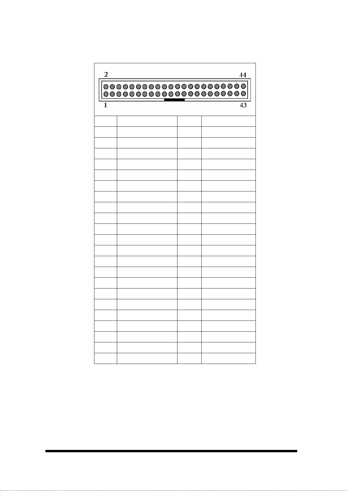
CN15: IDE Connector
The AW-E652 supports one 2.0mm pitch 44-pin pin header for up to two IDE devices.
Pin Define Pin Define
1 RSTPIDE# 2 Ground
3 PDD7 4 PDD8
5 PDD6 6 PDD9
7 PDD5 8 PDD10
9 PDD4 10 PDD11
11 PDD3 12 PDD12
16
13 PDD2 14 PDD13
15 PDD1 16 PDD14
17 PDD0 18 PDD15
19 Ground 20 NC
21 PDDREQ 22 Ground
23 PDIOW# 24 Ground
25 PDIOR# 26 Ground
27 PDIORDY 28 Ground
29 PDDACK# 30 Ground
31 IRQ14 32 V5P0
33 PDA1 34 PD66#
35 PDA0 36 PDA2
37 PDCS#1 38 PDCS#3
39 PIDELED 40 Ground
41 V5P0 42 V5P0
43 Ground 44 Ground
AW-E652
Page 22

17
CN16: LCD Backlight Connector
CN17: Floppy Connector
Pin Define Pin Define
User’s manual
Pin Define
1 V12P0
2 Ground
3 ENABKL
1 Ground 2 DEN0
3 Ground 4 NC
5 NC 6 DEN1
7 Ground 8 INDEX#
9 Ground 10 MTR#0
11 Ground 12 DS#1
13 Ground 14 DS#0
15 Ground 16 MTR#1
17 Ground 18 DIR#
19 Ground 20 STEP#
21 Ground 22 WDATA#
23 Ground 24 WGATE#
25 Ground 26 TRAK0#
27 Ground 28 WP#
29 Ground 30 RDATA#
31 Ground 32 HDSEL#
33 Ground 34 DSKCHG#
AW-E652
Page 23

User’s manual
CN18: USB3/4 Connector (Pin-Header)
The AW-E652 supports four USB ports, CN18 with 2.0mm pitch pin header for
USB3/4.
Pin Define Pin Define
1 5VUSB1 2 5VUSB1
3 USBDT2- 4 USBDT3-
5 USBDT2+ 6 USBDT3+
7 Ground 8 Ground
9 NC 10 Ground
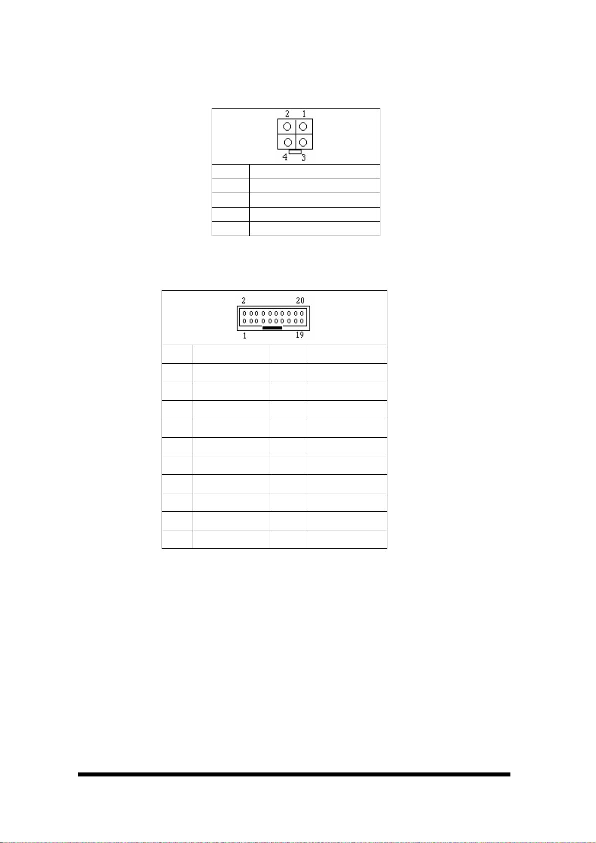
CN19: ATX Power Connector
18
CN20: AC97 Connector
Pin Define Pin Define
1 V12P0 2 Ground
3 Ground 4 AC97_BITCLK
5 V3P3 6 NC
7 AC97_DIN 8 AC97_SYNC
9 Ground 10 AC97_RST
Pin Define
1 5V_SB
2 PWR_TYPE
3 PS_ON#
11 AC97_DOUT 12 SPKR
AW-E652
Page 24
19
CN21: +5V/+12V Input Connector
CN22: COM3/COM4 Connector (Pin-Header 2.0mm)
User’s manual
Pin Define
1 V5P0
2 Ground
3 V12P0
4 Ground
Pin Define Pin Define
1 DCD3#IN 2 DSR3#IN
3 RXD3_IN 4 RTS#3OUT
5 TXD3_OUT 6 CTS3#IN
7 DTR#3OUT 8 RI3#_5V_12V
9 Ground 10 NC
11 DCD4#IN 12 DSR4#IN
13 RXD4_IN 14 RTS#4OUT
15 TXD4OUT 16 CTS4#IN
17 DTR#4OUT 18 RI4#_5V_12V
19 Ground 20 NC
AW-E652
Page 25

User’s manual
CN23: LCD Display Connector
Pin Define Pin Define
1 SPD1 2 SPCLK1
3 Ground 4 Ground
5 VCCLCD 6 VCCLCD
7 PCIRST 8 Ground
9 FP_D0 10 FP_D1
11 FP_D2 12 FP_D3
13 FP_D4 14 FP_D5
15 FP_D6 16 FP_D7
20
17 FP_D8 18 FP_D9
19 FP_D10 20 FP_D11
21 FP_D12 22 FP_D13
23 FP_D14 24 FP_D15
25 FP_D16 26 FP_D17
27 FP_D18 28 FP_D19
29 FP_D20 30 FP_D21
31 FP_D22 32 FP_D23
33 FP_D024 34 FP_D25
35 FP_CLK 36 FP_VS
37 FP_DEN 38 FP_HS
39 Ground 40 ENABKL
41 FP_D26 42 FP_D27
43 FP_D28 44 FP_D29
45 FP_D30 46 FP_D31
47 FP_D32 48 FP_D33
49 FP_D34 50 FP_D35
Note: The factory default at +3.3V, please make sure your
Panel Voltage setting by JP8
AW-E652
Page 26

21
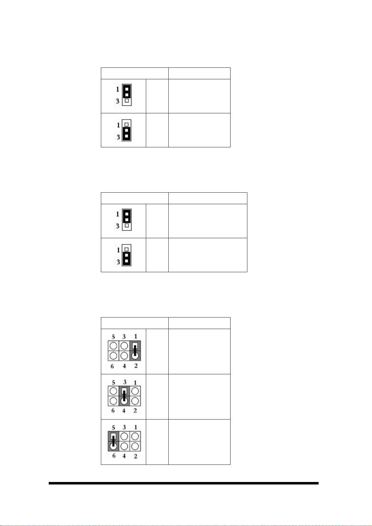
JP1: COM1 Voltage Select
Setting Define
User’s manual
1-2
(Default)
3-4
5-6
JP2: COM2 Mode Select (RS232/422/485)
Ring
5V
12V
Setting Define
1-2
3-4
5-6
RS-232
(Default)
RS-422
RS-485
AW-E652
Page 27
JP3: Clear CMOS
User’s manual
Setting Define
22
JP4: Watchdog Output Select
Setting Define
1-2
2-3
1-2
2-3
Hold Data
(Default)
Clear CMOS
IRQ11
Reset (Default)
JP5: RI/Voltage Select for COM2
Setting Define
1-2
3-4
5-6
RI
(Default)
+5V
+12V
AW-E652
Page 28

23
JP6: RI/Voltage Select for COM4
Setting Define
User’s manual
1-2
3-4
5-6
JP7: RI/Voltage Select for COM3
Ring
(Default)
5V
12V
Setting Define
1-2
3-4
5-6
Ring
(Default)
5V
12V
AW-E652
Page 29

JP8: LCD Voltage Select
Setting Define
User’s manual
24
1-2
2-3
JP9: COM2 RS485 Wire Select
Setting Define
1-2
2-3
+3.3V (Default)
+5V
2 wire
4 wire
AW-E652
Page 30

25
Chapter 3. BIOS Setup
The ROM chip of your AW-E652 board is configured with a customized Basic
Input/Output System (BIOS) from Phoenix-Award BIOS. The BIOS is a set of
permanently recorded program routines that give the system its fundamental
operational characteristics. It also tests the computer and determines how the
User’s manual
computer reacts to instructions that are part of programs.
The BIOS is made up of code and programs that provide the device-level control for
the major I/O devices in the system. It contains a set of routines (called POST, for
Power-On Self Test) that check out the system when you turn it on. The BIOS also
includes CMOS Setup program, so no disk-based setup program is required CMOS
RAM stores information for:
z Date and time
z Memory capacity of the main board
z Type of display adapter installed
z Number and type of disk drives
The CMOS memory is maintained by battery installed on the AW-E652 board. By
using the battery, all memory in CMOS can be retained when the system power switch
is turned off. The system BIOS also supports easy way to reload the CMOS data
when you replace the battery of the battery power lose.
3.1 Quick Setup
In most cases, you can quickly configure the system by choosing the following main
menu options:
1. Choose “Load Optimized Defaults” from the main menu. This loads the setup
AW-E652
Page 31

User’s manual
default values from the BIOS Features Setup and Chipset Features Setup screens.
2. Choose “Standard COS Features” from the main menu. This option lets you
configure the date and time, hard disk type, floppy disk drive type, primary
display and more.
3. In the main menu, press F10 (“Save & Exit Setup”) to save your changes and
reboot the system.
3.2 Entering the CMOS Setup Program
Use the CMOS Setup program to modify the system parameters to reflect the options
installed in your system and to customized your system. For example, you should
run the Setup program after you:
26
z Received an error code at startup
z Install another disk drive
z Use your system after not having used it for a long time
z Find the original setup missing
z Replace the battery
z Change to a different type of CPU
z Run the Phoenix-Award Flash program to update the system
BIOS
Run the CMOS Setup program after you turn on the system. On-screen
instructions explain how to use the program.
Enter the CMOS Setup program’s main menu as follows:
1. Turn on or reboot the system. After the BIOS performs a series of
diagnostic checks, the following message appears:
“Press DEL to enter SETUP”
2. Press the <DEL> key to enter CMOS Setup program. The main menu
appears:
AW-E652
Page 32

27
:
User’s manual
Phoeni x - Aw a r dB IO S CO S Se t u p Uti li ty
Standard CMOS Features
Advanced BIOS Features
Advanced Chipset Features
Integrated Peripherals
Power Management Setup
PnP/PCI Configurations
PC Health Status
Esc: Quit
Change CPU's Clock & Voltage
Freque nc y/ V o lt ag e Co ntrol
Load Fail-Safe Defaults
Load Optimized Defaults
Set Supe rv i s or Pas sw or d
Set User Pa s sw or d
Save & Exit Setup
Exit Without Saving
Select Ite m
3. Choose a setup option with the arrow keys and press <Enter>. See the
following sections for a brief description of each setup option.
In the main menu, press F10 (“Save & Exit Setup) to save your changes and
reboot the system. Choosing “EXIT WITHOUT SAVING” ignores your
changes and exits the program. Pressing <ESC> anywhere in the program
returns you to the main menu.
3.3 Menu Options
The main menu options of the CMOS Setup program are described in the following
and the following sections of this chapter.
STANDARD CMOS FEATURES:
Configure the date & time, hard disk drive type, floppy disk drive type, primary
display type and more
ADVANCED BIOS FEATURES:
Configure advanced system options such as enabling/disabling cache memory and
shadow RAM
AW-E652
Page 33

User’s manual
ADVANCED CHIPSET FEATURES:
Configure advanced chipset register options such DRAM timing
INTEGRATED PERIPHERALS:
Configure onboard I/O functions
POWER MANAGEMENT SETUP:
Configure power management features such as timer selects
PNP/PCI CONFIGURATION:
Configure Plug & Play IRQ assignments and PCI slots
PC HEALTH STATUS:
Configure the CPU speed and, if the optional Winbond W83627HF system monitor IC
is installed, view system information
28
FREQUENCY/VOLTAGE CONTROL
Use this menu to specify your settings for frequency/voltage control
LOAD FAIL-SAFE DEFAULT:
Loads BIOS default values. Use this option as diagnostic aid if your system behaves
erratically
LOAD OPTIMIZED DEFAULTS:
Use this menu to load the BIOS default values that are factory settings for optimal
performance system operations.
SET SUPERVISORS & USER PASSWORD:
Configure the system so that a password is required when the system boots or you
attempt to enter the CMOS setup program. When you log in with this password, you
will be able to enter the COS Setup main menu, but you can not enter other menus in
the CMOS Setup program.
SAVE & EXIT SETUP:
Save changes of values to CMOS and exit the CMOS setup program
EXIT WITHOUT SAVING:
Abandon all CMOS changes and exit the CMOS setup program
AW-E652
Page 34

29
F
C
User’s manual
Standard CMOS Features Setup
Use the Standard CMOS Setup option as follows:
1. Choose “Standard CMOS Features” from the main menu. The following screen
appears:
Phoeni x - Aw ard BIO S CM OS Set up Util it y
Standard CMOS Features
Date (mm:dd:yy) Fri, Aug 30 2002
Time (hh:mm:ss) 10 : 1 : 40
IDE Primary Master (ST51270A )
IDE Primary Slave (None)
IDE Second ar y Mast er (Non e)
IDE Secondary Slave (None)
Drive A (1.44MB, 3. 5 in .)
Drive B (None)
Video (EGA/VGA)
Halt On (All, But Keyboard)
Base Memory 640K
Extended M em or y 224736K
Total Memory 245760 K
Item Help
Menu Level
hange the day, month,
year and century
+/-/PU/PD:ValueEnter: Se le ct F10:Sa ve ESC: Exi t F1: General He lp
F6:Fail-Safe DefaultF5:Pre vi ou s V a lu e
7:Optimized Defaults
2. Use the arrow keys to move between fields. Modify the selected field using the
PgUP/PgDN/+/- keys. Some fields let you enter numeric values directly.
Option Description
Date (mm:dd:yy) Type the current date
Time (hour:min:sec) Type the current time (24-hour clock)
Hard Disks Choose from “Auto”, “User”, or “None”
If your drive is not one of the predefined types, choose “User”
and enter the following drive specifications:
Cylinders, heads, Wpcom, L-Zone, sectors, and mode
Consult the documentation received with the drive for the
values that will give you optimum performance.
AW-E652
Page 35

User’s manual
30
Drive A
Drive B
Video Choose: EGA/VGA
Halt On Controls whether the system stops in case of an error detected
Choose: None
360K, 5.25 in
1.2M, 5.25 in
720K, 3.5 in
1.44M, 3.5”
2.88M, 3.5”
CGA 40
CGA 80
Mono
during power up.
Choose: All Errors (Default)
No Errors
All, But Keyboard
All, But Diskette
All, But Disk/Key
3. After you have finished with the Standard CMOS Features program, press the
<ESC> key to return to the main menu.
AW-E652
Page 36
31
F
User’s manual
Advanced BIOS Features Setup
Use the Advanced BIOS Features Setup option as follows:
1. Choose “Advanced BIOS Features Setup” from the main menu. The following
screen appears:
Phoeni x - AW a r dB IO S CM OS Se t up Util ity
Virus Warning <Disabled>
CPU Internal Cache <Enabled>
External Cache <Enabled>
CPU L2 Cache FCC Checking <Enabled>
Processor Number Feature <Enabled>
Quick Power On Self Test <Enabled>
First Boot Device <Floppy>
Second Boot Device <HDD-0>
Third Boot Device <Ls120>
Boot Other Device <Enabled>
Swap Floppy Drive <Disabled>
Boot Up Floppy Seek <Enabled>
Boot Up Numlock Status <On>
Gate A20 Option <Fast>
Typematic Rate Setting <Disabled>
X Typematic Rate (Chars/Sec) 6
X Typema ti c De la y (M se c) 250
Security Option <Setup>
OS Select For DRAM > 64MB <Non-OS2)
Video BIOS Shadow <Enabled>
C8000-CBFFF Shadow <Disabled>
CC000-CFFFF Shadow <Disabled>
D0000-D3FFF Shadow <Disabled>
D4000-D7FFF Shadow <Disabled>
D8000-DBFFF Shadow <Disabled>
DC000-DFFFF Shadow <Disabled>
Small Logo (EPA) Show <Disabled>
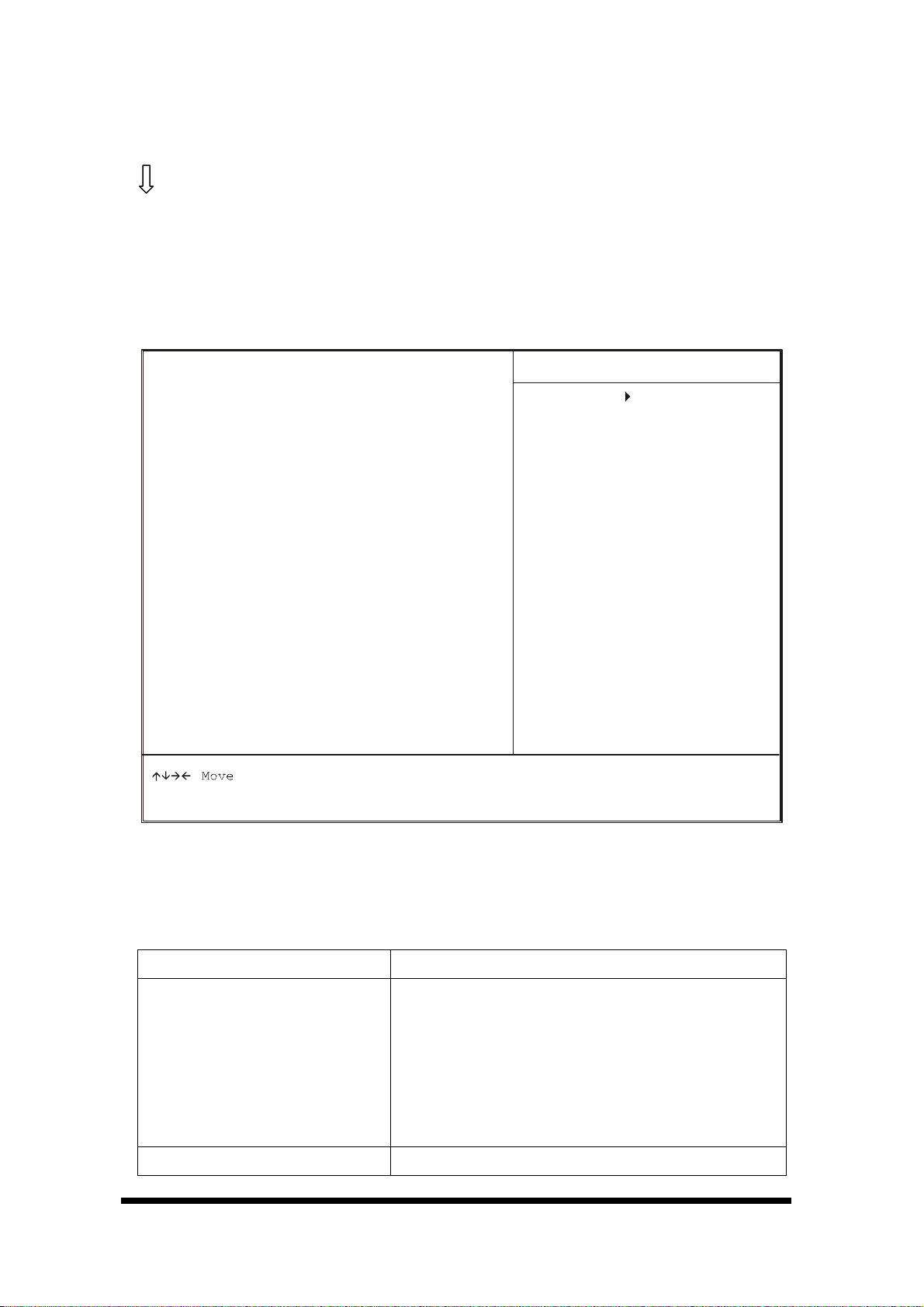
Advanced BIOS Features
Item Help
Menu Level
Allow yo u to cha nge
the VIRU S w a rn in g
featur e fo r ID E Ha rd
Disk boot sector
protec ti on . If thi s
function is enabled
and some on e at te mp t to
write da ta int o this
area. BIOS will show
a warnin g m e ss ag e on
screen and alarm beep
+/-/PU/PD:ValueEnter: Se le ct F10:Sa ve ESC: Exi t F1: General He lp
F6:Fail-Safe DefaultF5:Pre vi ou s V a lu e
7:Optimized Defaults
2. Use the arrow keys to move between items and to select values. Modify the
selected fields using the PgUP/PgDN keys. Press the <F1> “Help” key for
information on the available options:
Option Description
Virus Warning When enabled, any attempt to write to the boot
sector and partition table will halt the system and
cause a warning message to appear. If this
happens, you can use an anti-virus utility on a
virus-free, bootable floppy disk to reboot and clean
your system. The default setting is Disabled.
CPU Internal/External Cache Cache memory is an additional memory that is
AW-E652
Page 37

User’s manual
much faster than the conventional DRAM (system
memory). CPUs with 486-type contain internal
cache memory; most PCs have external cache
memory. When CPU requests data, the system
transfers the data from the main DRAM into cache
memory, for even faster access by the CPU. The
External Cache wouldn’t appear if the system using
does not have external cache memory.
Choose: Enabled / Disabled
CPU L2 Cache FCC Checking When enabled, memory checking is enabled when
the external cache contains ECC SRAMs.
Choose: Enabled / Disabled
32
Processor Number Feature
Quick Power on Self Test
First/Second/Third Boot Device The BIOS attempts to load the operating system
Boot other Device
This is for Pentium III processor. When enabled, it
will check the CPU serial number. If users don’t
want the system to know the serial number, you
could disable this option.
Choose: Enabled / Disabled
When enabled, the reducing time required runs the
power-on-self-test (POST); a quick POST could
skip certain steps. We recommend users disable
quick POST normally.
Choose: Enabled / Disabled
from the devices in the sequence selected in these
items.
Choose: Floppy, LS-120, HDH-0, 1, 2, 3, SCSI,
CDROM, ZIP100, USB-FDD, USB-ZIP,
USB-CDROM, USB-HDD, LAN, Disabled
If your boot device is not included in the following
Swap Floppy Drive
choices of Floppy---LS120, HDD0, HDD1, HDD2,
SCSI, CDROM---you may set First/Second/Third
Boot devices to disable and enable the “Boot Other
Device” function. The system will automatically
boot the other device.
Choose: Enabled / Disabled
This would be effective only in systems with two
floppy drives. To select enable assigns physical
drive B to logical drive A, and physical drive A to
AW-E652
Page 38

33
p
User’s manual
logical drive B.
Choose: Enabled / Disabled
Boot Up Floppy Seek
Boot Up NumLock Status Choose On or Off. On puts the numeric keypad in
Gate A20 Option Choose Enabled or Disabled. Enable this option to
Type matic Rate Setting Choose Enabled or Disabled. Enable this option to
When enabled, the BIOS seeks floppy drives to
decide the tracks—40 or 80. 360KB floppy drives
have 40 tracks; 720KB floppy drives, 1.2MB, and
1.44MB capacity all have 80 tracks. Few modern
PCs have 40-tracks floppy drives; therefore, we
recommend that you would disable this option to
save time.
Choose: Enabled / Disabled
Num Lock mode at boot-up. Off puts the numeric
keypad in arrow key mode at boot-up
allow RAM accesses faster than normal, and is
useful in networking operating systems.
adjust the keystroke repeat rate. Adjust the rate
via Typematic Rate Delay and Typematic Rate
Typematic Rate (Chars/Sec) Choose the rate at which character keeps repeating
Typematic Delay (Msec) Choose the delay between holding down a key and
when the character begins repeating
Security Option Choose Setup or System. This lets you specify
whether a password is required every time the
system boots or only when an attempt is made to
enter the CMOS Setup program.
“Setup” – The password prompt only appears if you
attempt to enter the CMOS setup program.
“System” – The password prompt appears each time
the system is booted.
Note: The password function is disabled by
default. For a description of enabling the
assword function, refer to the section: Supervisor
Password & User Password later in this chapter.
OS Select for DRAM > 64MB Set to OS/2 if your system is using OS/2 and has a
memory size of more than 64MB
Small Logo
Choose: Enabled / Disabled
AW-E652
Page 39

User’s manual
34
Advanced Chipset Features Setup
Use the Advanced Chipset Features Setup option as follows:
1. Choose “Advanced Chipset Features Setup” from the main menu. The following
screen appears:
Phoeni x - Aw a r dB IO S CM OS Se t up Util ity
DRAM Timing By SPD <Enabled>
X DRAM Clock Host CLK
X SDRAM Cy cl e Le ng th 3
X Bank Interleave Disabled
Memory Hole <Disabled>
P2C/C2P Co n c ur re nc y <Enabled>
System BIO S Ca ch ea bl e <Disable d>
Video RAM Cacheable <Disab le d>
Frame Buff e r Siz e <8M>
AGP Apertu r e Siz e <64M>
AGP-4X Mode <Enabled>
Panel Type <07>
Boot Device Select <Auto>
OnChip USB <Enabled>
USB Keyboard Support <Disabled>
OnChip Sound <Auto>
OnChip Modem
CPU to PCI Write Buffer <Enabled>
PCI Dynami c Bu rs ti ng <Enabled>
PCI Master 0 WS Write <Enabled>
PCI Delay Transaction <Disabled>
PCI#2 Access #1 Retry <Enabled>
AGP Master 1 WS Write <Disabled>
AGP Master 1 WS Read <Disabled>
F5:Pre vi ou s Va lu e
Advanced Chipset Features
Menu Level
+/-/PU/PD:ValueEnter:Select
F6:Fail-Safe Default
F10:Save
Item Help
ESC: Exit
F7:Optimized Defaults
F1: Gene ra l He lp
2. Move between items and select values by using the arrow keys. Modify the
selected fields using the PnUP/PgDN keys. For information on the various
options, press <F1> key.
AW-E652
Page 40

35
User’s manual
Option Description
DRAM Timing By SPD
DRAM Clock
SDRAM Cycle Length
Bank Interleave Choose: 2 Bank / 4 Bank / Disabled
Memory Hole At 15M-16M Choose Enabled or Disabled. You can reserve this
P2C/C2P Concurrency
It lets you select the value in this field, depending
on the board paged DRAMs or EDO (Extended
Data Output) DRAMS.
Choose: Enabled / Disabled
It lets you control the DRAM speed.
Choose: Host Clock, HCLK-33M, HCLK+33M
It sets the CAS latency timing.
Choose: 3 / 2
area of system memory for ISA adapter ROM.
When this area is reserved, it cannot be cached.
The user information of peripherals that need to use
this area of system memory usually discusses their
memory requirement.
It lets you enable or disable the PIC to CPU or CPU
System BIOS Cacheable Choose Enabled or Disabled. When enabled,
Video RAM Cacheable Choose: Enabled / Disabled
Frame Buffer Size Choose: 2M / 4M / 8M / 16M / 32M
AGP Aperture Size (MB) Select the size of AGP aperture. The aperture is a
AGP-4X Mode
to PCI.
Choose: Enabled / Disabled
caching of the system BIOS at F0000h-FFFFFh,
enhancing system performance. However, if any
program writes to this memory area, a system error
may result.
portion of the PCI memory address range dedicated
for graphics memory address space. Host cycle
that hit the aperture range are forwarded to the AGP
without any translation. 64MB
When 4X mode enabled, it will enhance your
system performance.
OnChip USB
Choose: Enabled / Disabled
You could enable this function if the system
contains USB (Universal Serial Bus) controller and
USB keyboard. When disabled, the system will
not be able to access USB keyboard.
AW-E652
Page 41

User’s manual
b
b
Choose: Enabled / Disabled
36
USB Keyboard Support
OnChip Sound
CPU to PCI Write Buffer
PCI Dynamic Bursting
You could enable this function if the system
contains USB controller and USB keyboard.
Choose: Enabled / Disabled
It lets you control the onboard VIA 1611 audio.
Choose: Auto / Disabled
When enabled, writes from CPU to PCI bus are
uffered. It also compensate the speed differences
Between the CPU and PCI bus. Otherwise, when
disabled, the writes are not buffered. The CPU
must wait until the write is completed starting
another write cycle.
Choose: Enabled / Disabled
When enabled, each write transaction goes to the
write buffer. Then, burstable transactions burst on
the PCI bus and nonburstable truncations don’t.
Choose: Enabled / Disabled
PCI Master 0 WS Write
PCI Delay Transaction
PCI#2 Access #1 Retry
AGP Master 1 WS Write
AGP Master 1 WS Read
When enabled, writes to the PCI bus are executed
with zero waiting states.
Choose: Enabled / Disabled
The chipset with an embedded 32-bit posted write
uffer supports delay transaction cycles. Choose
“enable” to support compliances with PCI
specification, version 2.1.
Choose: Enabled / Disabled
When enabled, PCI#2 will be unconnected if max
retries attempt to be without success.
Choose: Enabled / Disabled
When enabled, the system will run single wait state
delay before writing data from buffer; if users
disable the system, it will run twice wait states and
the system can be stable.
Choose: Enabled / Disabled
When enabled, the system will run single wait state
delay before reading data from buffer; if users
disable the system, it will run twice wait states and
the system can be stable.
Choose: Enabled / Disabled
AW-E652
Page 42

37
F
User’s manual
Integrated Peripherals
Use the Integrated Peripherals Setup option as follows:
1. Choose “Integrated Peripherals Setup” from the main menu. The following
screen appears:
2. Move between items and select values by using the arrow keys. Modify the
selected fields using the PgUP/PgDN keys. Please press the <F1> key for
information on the various options.
Phoeni x - Aw ar dB IO S CM OS Se tup Utility
Integrated Peripherals
On-Chip IDE Channel0 <Enabled>
On-Chip IDE Channel1 <Enabled>
IDE Prefetch Mode <Enabled>
Primary Master PIO <Auto>
Primary Slave PIO <Auto>
Secondary Master PIO <Auto>
Secondary Slave PIO <Auto>
Primary Master UDMA <Auto>
Primary Slave UDMA <Auto>
Secondary Master UDMA <Auto>
Secondary Slave UDMA <Auto>
Init Display First <AGP>
IDE HDD Block Mode <Enabled>
Onboard FD D Co nt ro ll er <Enabled>
Onboard Se ri al Por t 1 <3F8/IRQ 4>
Onboard Se ri al Por t 2 <2F8/IRQ 3>
UART 2 Mode <Standard>
X IR Function Duplex Half
x TX RX inverting enable No, Yes
Onboard Parallel Port <378/IRQ7>
Onboard Parallel Mode <Normal>
X ECP Mode Use DMA 3
X Parall el Por t EP P Ty pe EPP1.9
F5:Pre vious Value
Enter:Select
+/-/PU/PD:Value
F6:Fail-Safe Default
Menu Level
F10:Save
Item Help
ESC: Exit
7:Optimized Defaults
F1: General He lp
AW-E652
Page 43

User’s manual
Option Description
38
On-Chip IDE Channel 0
On-Chip IDE Channel 1
IDE Prefetch Mode
IDE Primary/Secondary
The system chipset contains a PIC IDE interface, which
supports two IDE channels. When enabled, it will
activate the primary and/or secondary IDE interface.
When disabled, it will deactivate the interface.
Choose: Enabled / Disabled
The system chipset contains a PCI IDE interface, which
supports two IDE channels. When enabled, it will
activate the secondary IDE interface. When disabled,
it will deactivate the interface.
Choose: Enabled / Disabled
The onboard IDE drive interfaces support IDE prefetch,
which are faster drive accesses. If the interface
doesn’t support prefetch, users could choose “disable”
when installing the primary and/or secondary add-in
IDE interface.
Choose: Enabled / Disabled
Auto/Mode0/Mode1/Mode2/Mode3/Mode4
Master/Slave PIO
IDE Primary/Secondary
Master/Slave UDMA
Init Display First Default: Onboard/AGP
IDE HDD Block Mode Enabled/Disabled the IDE HDD Block Mode function.
The four IDE PIO (Programmed Input/Output) fields let
you set a PIO mode (0-4) for each of the four IDE
devices that the onboard IDE interface supports.
Modes 0 through 4 provide successively increased
performance. In Auto mode, the system automatically
determines the best mode for each device.
Auto, Mode0, Mode1, Mode2, Mode3, Mode4
UltraDMA33/66/100 implementation is possible only if
your IDE hard drive supports it and the operating
environment includes a DMA driver. If your hard
drive and your system software both support
UltraDMA33/66/100, select Auto to enable BIOS
support.
This option lets you choose the priority of AGP & PCI
VGA card
Note: Not all drives support this function
Onboard FDC Controller Enabled/Disabled. Select enabled if your system has a
floppy disk controller installed on the system board and
AW-E652
Page 44

39
Onboard Serial Port1/2 Choose: 3F8/IRQ4, 2F8/IRQ3
User’s manual
you wish to use it. If the system has no floppy drive,
select Disabled in this field.
Select an address and corresponding interrupt for the
first and second serial ports.
UART 2 Mode
Select an operating mode for the second serial port:
Normal RS-232C serial port
Standard RS-232C serial port
IrDA 1.0 Infrared port compliant with
IrDA 1.0 specification
IrDA SIR IrDA-compliant serial
Infrared port
IrDA MIR 1 MB/sec infrared port
IrDA FIR Fast infrared standard
FIR Fast infrared standard
MIR 0.57M 0.57 MB/sec infrared port
MIR 1.15M 1.15 MB/sec infrared port
Sharp IR 4 MB/sec data transmission
HPSIR IrDA-compliant serial
infrared port
ASKIR Amplitude shift keyed
IR Function Duplex
TX RX inverting enable
Onboard Parallel Port Choose: 378/IRQ7
Parallel Port Mode Default Setting: SPP
ECP Mode Use DMA
Choose the requiring value of the IR device and
connect to the IR port. Full duplex mode allows two
directions transmission simultaneously. Half duplex
mode allows only one direction at the same time.
Choose: Full / Half
Check your IR peripheral documentation to select the
correct setting.
Choose: Yes/No, Y es/Yes, No/Y es, No/No
This option lets you to determine onboard parallel port
controller I/O address setting.
Select an operating mode for the onboard parallel port.
Select a DMA channel for the port
Choose: 3 / 1
infrared port
AW-E652
Page 45

User’s manual
40
Parallel Port EPP Type
Select EPP port type 1.7 or 1.9
Choose: EPP1.9 / EPP1.7
AW-E652
Page 46

41
F
User’s manual
Power Management Setup
The Power Management Setup controls the board’s “green” features. To save energy
these features shut down the video display and hard disk drive.
Use the Power Management Setup option as follows:
1. Choose “Power Management Setup” from the main menu. The following screen
appears.
Phoenix - Aw ardB IO S CMOS Set up Utili ty
ACPI Function <Enabled>
Power Manage me nt <Press Ent er >
PM Control by APM <Yes>
Video Off Option <Suspend -> Off>
Video Off Method <V/H SYNC+Blank>
MODEM Use IRQ <3>
Soft-Off by PWRTBN <Instant-Off>
Wake Up Events <Press Enter >
Power Mana ge me nt Set up
Menu Level
+/-/PU/PD:Valu eEnter:Select
F6:Fail-Safe DefaultF5:Previou s Valu e
F10:Save ESC: Exit
Item Help
F1: Genera l Help
7:Optimized Defaults
2. Move between items and select values by using the arrow keys. Modify the
selected field the PgUP/PgDN keys. For information on the various options,
press <F1> key.
Option Description
ACPI Function Enables/Disables the ACPI function
Power Management Choose Disable, User Define, Min Saving or Max.
Saving.
“User Define” – Lets you specify when the HDD
and system will shut down
“Min Saving” - Predefine timer value of 4-12 min.
“Max Saving” – Predefine timer value of 1 minute
PM Control by APM
When the advanced power management is installed
on the system, users would select “Yes” to save
more power.
Choose: Yes / No
Video off Option
Select the power saving modes when the monitor is
blank.
AW-E652
Page 47

User’s manual
Always on Monitor remains “on” during
power saving modes.
Suspend-off, Monitor is blank when
system is in suspension mode
Suspend, Off monitor is blank when the
Standby-off system is in either suspension
or standby mode.
All modes-off Monitor is blank when the
system is in any power
saving mode.
Video Off Method Choose V/H SYNC+Blank, DPMS, Blank Screen
When power management blanks the screen and
turns off vertical and horizontal scanning.
The DPMS (Display Power Management System)
42
setting allows the BIOS to control the video card if
it has the DPMS features. If you don’t have a
Green monitor, use the Blank Screen option
MODEM Use IRQ Choose the IRQ used by the modem.
Default: Disabled
3. After you have finished with the Power Management Setup, press the <ESC> key
to return to the main menu.
AW-E652
Page 48

43
F
User’s manual
PNP/PCI Configuration
This option is used to configure Plug and Play assignments and route PCI interrupts to
designated ISA interrupts.
Use the PNP/PCI Configuration Setup option as follows:
1. Choose “PNP/PCI Configuration Setup” from the main menu, the following
screen appears.
Phoeni x - A w ar dB IO S CM OS S et up Uti lity
PNP OS Installed <No>
Reset Conf ig ura tio n Da te <Di sa bl ed>
Resource s Co ntr oll ed By <Au do (E SCD )>
X IRQ Reso urces Press Ent er
X DMA Reso urces Press Ent er
PCI/VGAS Palette Snoop <Disabled>
Assign IRQ For VGA <Enabled>
Assign IRQ For USB <Enalbed>
PnP/PCI Configurations
Menu LevelMenu Level
Select Yes i f yo u ar e
using a Pl ug and Pla y
capabl e op erating
system Select No if
you need the BIOS to
config ur e non-boot
devices
+/-/PU/PD:ValueEnter:Select
F6:Fail-Safe DefaultF5:Pre vi ou s Va l u e
F10:Save ESC: Exit
Item Help
F1: Gene ra l He lp
7:Optimized Defaults
2. Move between items and select values by using the arrow keys. Modify the
selected fields using the PgUP/PgDN keys. For information on the various
options, please press <F1> key.
Option Description
PNP OS Installed
Choose “Yes” when the system operating environment
is “Plug and Play aware”, for example, Win95.
Choose “No” if users need the BIOS to configure
non-boot devices.
Choose: Yes / No
Reset Configuration Data Choose Enable or Disable
“Enable” – PNP configuration data is reset in BIOS
“Disable” – PNP configuration date is retained in BIOS
Resources Controlled By Choose Auto or Manual. This option specifies
whether resources are controlled by automatic or
manual configuration
IRQ Resources IRQ-3 Assigned to <PCI Device>
AW-E652
Page 49

User’s manual
F
IRQ-4 Assigned to <PCI Device>
IRQ-5 Assigned to <PCI Device>
IRQ-7 Assigned to <PCI Device>
IRQ-9 Assigned to <PCI Device>
IRQ-10 Assigned to <PCI Device>
IRQ-11 Assigned to <PCI Device>
IRQ-12 Assigned to <PCI Device>
IRQ-14 Assigned to <PCI Device>
IRQ-15 Assigned to <PCI Device>
44
DMA Resources
Assigning every DMA channel a type when resources
are controlled manually. This would depend on the
type of device using the DMA channel.
PCI/VGA Palette Snoop Enabling this item informs the PCI/VGA card to keep
silent when palette register is updated
Assign IRQ for VGA Choose Enabled/Disabled to specify whether the VGA
uses on IRQ or not.
Assign IRQ for USB Choose Enabled/Disabled to specify whether the USB
uses an IRQ or not.
3. Please press the <ESC> key to return the main menu after finishing with the
PNP/PCI Configuration Setup.
PC Health Status Configuration Setup
Choose “PC Health Status Configuration Setup” from the main menu, the following
screen appears:
Phoeni x - Aw a r dB IO S Se tu p Utility
Current CPU Temp. 30/86
Current CPUFAN Speed 31/87
Vcore 1.16 V
2.5V 2.61 V
3.3V 3.38 V
5V 5.30 V
12V 15.54 V
PC Health Status
+/-/PU/PD:ValueEnter:Select F10:Save
F6:Fail-Safe DefaultF5:Pre vi ou s Va l u e
AW-E652
Item Help
Menu LevelMenu Level
ESC: Exit
F1: Gene ra l He lp
7:Optimized Defaults
Page 50
45
F
User’s manual
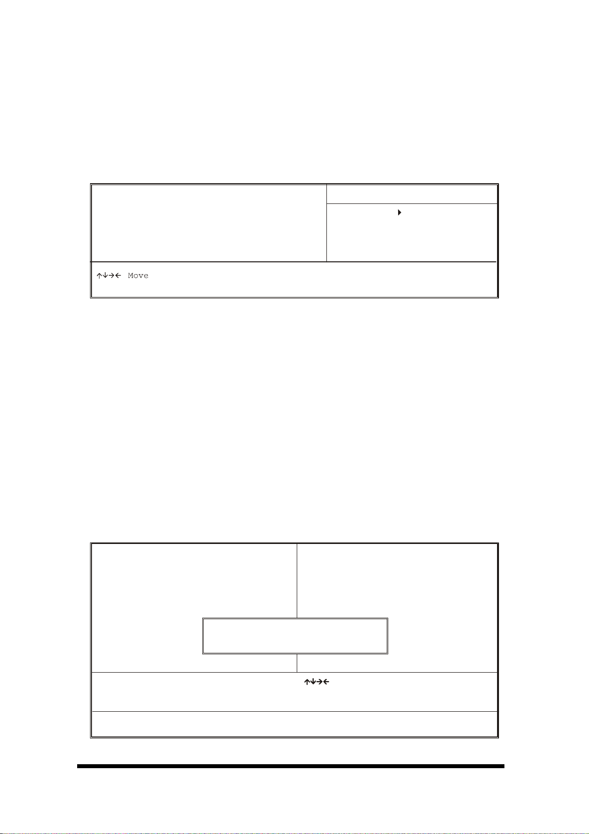
Frequency/Voltage Control Option
Choose the “Frequency/Voltage Control” from main menu, the following screen
appears:
Phoeni x - A w ar dB IO S CM OS S et up Uti lity
Frequency/Voltage Control
VIA C3 Clock Ration <Default>
Auto Detect DIMM/PCI Clk <Enabled>
Spread Spectrum Modulated <Disabled>
CPU Host Clock (CPU/PCI) <Defualt>
Enter:Select F10:Save ESC: Exit F1: General Help
+/-/PU/PD:Value
F6:Fail-Safe DefaultF5:Pre vi ou s Value
Menu LevelMenu Level
This item is for VIA
C3 CPU Ratio
adjustment
Item Help
7:Optimized Defaults
Load Fail-Safe Defaults
This option loads the troubleshooting default values permanently stored in the BIOS
ROM. This is useful if you are having problems with the main board and need to
debug or troubleshoot the system. The loaded default settings do not affect the
Standard CMOS Setup screen.
To use this feature, highlight it on the main screen and press <Enter>. A line will
appear on the screen asking if you want to load the BIOS default values. Pres the
<Y> key and then press <Enter> if you want to load the BIOS default.
Poenix - AwardBIOS CMOS Setup Utility
Standard CMOS Features
Advanced BIOS Features
Advanced Chipset Features
Integrated Peripherals
Power Ma na ge ment
PnP/PC I Co nf iguration
PC Health Status
Esc : Quit
F10 : Save & Exi t Se tu p
Load Fail-Safe Defaults (Y/N)? N
Time, Da te, Hard Disk Type .. .
Time, Da te, Hard Disk Type .. .Time, Da te, Hard Disk Type .. .Time, Da te, Hard Disk Type .. .Time, Da te, Hard Disk Type .. .
Frequency/Volage Control
Load Fail-Safe Defaults
Load Optimized Defaults
Set Supe rv is or P as sw or d
Set User Pas sw o r d
Save & Exit Setup
Exit Without Saving
: Select Item
(Shift)F2: Change Color
AW-E652
Page 51

User’s manual
46
Load Optimized Defaults
This option loads optimized settings stored in the BIOS ROM. The auto-configured
settings do not affect the Standard CMOS Setup screen.
To use this feature, highlight it on the main screen and press <Enter>. A line will
appear on the screen asking if you want to load the Optimized Default Values. Press
the <Y> key and then press <Enter> if you want to load the SETUP default.
Phoeni x - Aw ardBIOS CMOS Set up Ut il it y
Standard CMOS Features
Advanced BIOS Features
Advanced Chipset Features
Integrated Peripherals
Power Ma na ge ment
PnP/PC I Co nf iguration
PC Health Status
Esc : Quit
F10 : Save & Exi t Se tu p
Load Optimized Defaults (Y/N)? N
Time, Da te, Hard Disk Type .. .
Time, Da te, Hard Disk Type .. .Time, Da te, Hard Disk Type .. .Time, Da te, Hard Disk Type .. .Time, Da te, Hard Disk Type .. .
Frequency/Volage Control
Load Fail-Safe Defaults
Load Optimized Defaults
Set Supe rv is or P as sw or d
Set User Pas sw o r d
Save & Exit Setup
Exit Without Saving
: Select Item
(Shift)F2: Change Color
Supervisor/User Password
The password options let you prevent unauthorized system boot-up or unauthorized
use of CMOS setup. The Supervisor Password allows both system and CMOS Setup
program access; the User Password allows access to the system and the CMOS Setup
Utility main menu.
The password functions are disabled by default. You can use these options to enable
a password function or, if a password function is already enabled, change the
password.
To change a password, first choose a password option from the main menu and enter
the current password. Then type your new password at the prompt. The password
is case sensitive and you can use up to 8 alphanumeric characters. Press <Enter>
after entering the password. At the Next Prompt, confirm the new password by
AW-E652
Page 52

47
User’s manual
typing it and pressing <Enter> again.
Phoeni x - Aw ardBIOS CMOS Set up Ut il it y
Standard CMOS Features
Advanced BIOS Features
Advanced Chipset Features
Integrated Peripherals
Power Ma na ge ment
PnP/PC I Co nf iguration
PC Health Status
Esc : Quit
F10 : Save & Exi t Se tu p
Enter Password:
Time, Da te, Hard Disk Type .. .
Time, Da te, Hard Disk Type .. .Time, Da te, Hard Disk Type .. .Time, Da te, Hard Disk Type .. .Time, Da te, Hard Disk Type .. .
Frequency/Volage Control
Load Fail-Safe Defaults
Load Optimized Defaults
Set Supe rv is or P as sw or d
Set User Pas sw o r d
Save & Exit Setup
Exit Without Saving
: Select Item
(Shift)F2: Change Color
After you use this option to enable a password function, use the “Security Option” in
“BIOS Feature Setup” to specify whether a password is required every time the
system boots or only when an attempt is made to enter the CMOS Setup program.
Save and Exit Setup
This function automatically saves all CMOS values before exiting Setup.
Phoeni x - Aw ard BIO S CM OS Set up
Standard CMOS Features
Advanced BIOS Features
Advanced Chipset Features
Integrated Peripherals
Power Ma na ge ment
PnP/PC I Co nf iguration
PC Health Status
Esc : Quit
F10 : Save & Exi t Se tu p
Time, Da te, Hard Disk Type .. .
Frequency/Volage Control
Load Fail-Safe Defaults
Load Optimized Defaults
Set Supe rv is or P as sw or d
Set User Pas sw o r d
Save & Exit Setup
Exit Without Saving
: Select Item
(Shift)F2: Change Color
AW-E652
Page 53

User’s manual
Exit Without Saving
Use this function to exit Setup without saving the CMOS value.
Phoeni x - Aw ardBIOS CMOS Set up Ut il it y
48
Standard CMOS Features
Advanced BIOS Features
Advanced Chipset Features
Integrated Peripherals
Power Ma na ge ment
PnP/PC I Co nf iguration
PC Health Status
Esc : Quit
F10 : Save & Exi t Se tu p
Frequency/Volage Control
Load Fail-Safe Defaults
Load Optimized Defaults
Set Supe rv is or P as sw or d
Set User Pas sw o r d
Save & Exit Setup
Exit Without Saving
: Select Item
(Shift)F2: Change Color
Time, Da te, Hard Disk Type .. .
Time, Da te, Hard Disk Type .. .Time, Da te, Hard Disk Type .. .Time, Da te, Hard Disk Type .. .Time, Da te, Hard Disk Type .. .
AW-E652
Page 54

49
Chapter 4. Driver Utility
The system driver installation procedure must be performed first.
1. Insert the AW-E652 CD-ROM driver into the CD-ROM Drive
2. Select the Drivers\system file to click the Setup icon.
3. Click Next
User’s manual
AW-E652
Page 55

4. Click Yes
User’s manual
50
5. Select Normally Install, and then click Next
AW-E652
Page 56

51
6. Remain the default setting, and then click Next
User’s manual
7. Click Next
AW-E652
Page 57
User’s manual
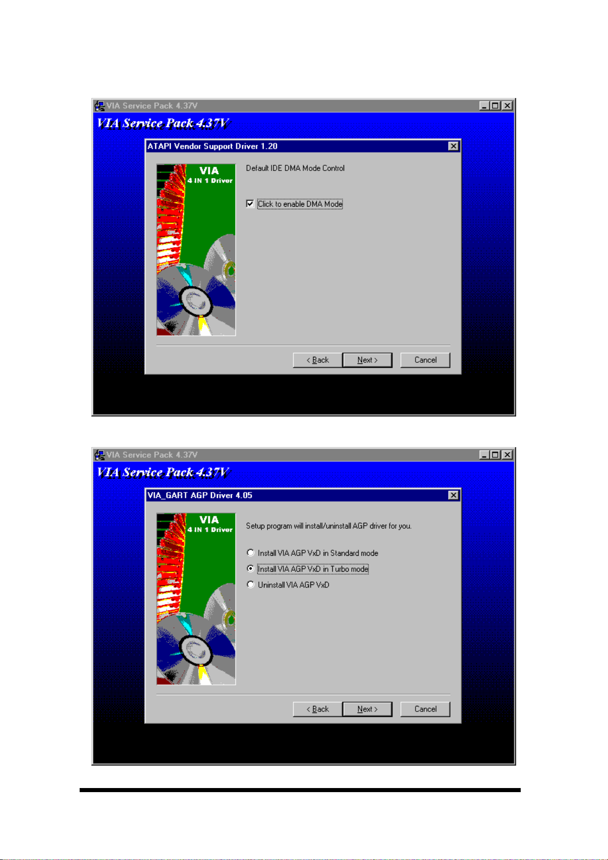
8. As the following picture, click Next
52
9. Select Install VIA AGP VxD in T urbo Mode, and click Click
AW-E652
Page 58

53
10. Click Next
User’s manual
11. Click Finish
AW-E652
Page 59

User’s manual
Installation process is completed and allowed the system to reboot.
Audio Driver Installation
1. Insert the AW-E652 CD ROM into the CD-ROM Drive
2. Select the Drivers\audio\ad1881 file to click the Setup icon
54
AW-E652
Page 60

55
User’s manual
(3) Click Next
(4) Click “OK”
AW-E652
Page 61

User’s manual
VGA Driver Installation
1. Install the AW-E652 CD ROM into the CD-ROM Drive
2. Select the Drivers\vga\Win9x ME file to click the Setup icon
A driver installation screen will appear, please follow the onscreen instruction to
install the driver in sequence
56
AW-E652
Page 62

57
3. At last, click Next
User’s manual
4. Click Next
Installation process is completed and allowed the system to reboot
AW-E652
Page 63

User’s manual
Ethernet Driver Installation
1. Insert the AW-E652 CD ROM into the CD-ROM Drive
2. Click the Start button
3. Select the Setting item
4. Click the Control Panel item
5. Select the Systems icon to open the System Properties box
6. Click the Device Manager tab
58
AW-E652
Page 64

59
7. Select the Network Adapters item
User’s manual
Another file will appear below this file, and then click on the file
8. Click the Driver Tab
9. Click the Update Driver Button
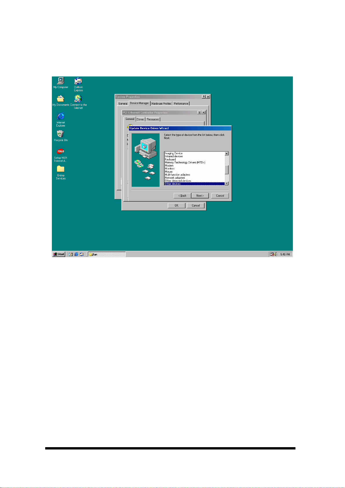
The Update Device Driver Wizard will appear
AW-E652
Page 65

User’s manual
60
10. Click Next
AW-E652
Page 66
61
11. Select CD ROM Drive, Drivers\lan\Win98, and click Next
Notice: We take the LAN installation under Win98 for example only, please choose
the file depending on your Windows OS.
User’s manual
AW-E652
Page 67

User’s manual
62
AW-E652
Page 68

63
User’s manual
Click Next
AW-E652
Page 69

Click Finish
User’s manual
64
Installation process is completed shutdown the computer and will allow the system to
reboot
AW-E652
Page 70

65
Appendix A: Programming the Watchdog Timer
The AW-E652 provides a watchdog timer that resets the CPU or generates an interrupt
if processing comes to a stop. This function ensures greater system reliability in
industrial stand-alone and unmanned environments.
In order to enable the watchdog timer, you have to output the value of the watchdog
timer interval to the controller. The value range is from 01H to FFH, and the related
time watchdog timer interval is 1 sec to 255 sec.
User’s manual
Data Timer interval
00 Disabled
01 1 sec
02 2 sec
* *
* *
FF 255 sec
If you want to program the watchdog timer, you must write timer value to I/O port
444 (hex).
For example:
ASSEMBLY LANGUAGE
Start Watchdog Timer DOS Debug
MOV DX, 444H OUT 444, XX
MOV AL, XXH
OUT DX, AL
Stop Watchdog Timer DOS Debug
MOV DX, 441H IN 441
IN AL, DX
Note: “XX” timer value
AW-E652
Page 71

Appendix B: Audio Kit
1. Board Layout
User’s manual
66
2.Board Dimension
Board Dimension (mil)
AW-E652
Page 72

67
3.Location of Connectors
User’s manual
4.List of Connectors
Connectors Description
CN1 Micro-Phone Input
CN2 Line-In
CN3 Speaker-Out
CN4 CD Audio Input
CN5 AC97 Audio Input
CN1: This MIC-In jack connects to a microphone
CN2: This Line-In jack connects to a tape player or other audio sources.
CN3: This Speaker-Out jack connects to a headphone or a speaker.
AW-E652
Page 73

User’s manual
CN4: CD Audio Input Connector
234
1
CN5: AC-97 Audio Input Connector
68
Pin Signal
1 CD AIDIO-L
2 GND
3 GND
4 CD AUDIO-R
Pin
1 +12V 2 GND
3 GND 4 AC97-BTCLK
5 +3.3V 6 KEY PIN
7 AC97-SDIN0 8 AC97-SYNC
9 GND 10 AC97-RESET
11 AC97-SDOUT 12 PC-BEEP
Signal
Pin
Signal
AW-E652
Page 74

69
Appendix C: Installing PC/104 Modules
The AW-E652 provides the standard PC/104 connector to give you the flexibility to
attach PC/104 module.
Please follow these steps to install the PC/104 modules to the AW-E652:
1. Set all jumpers or switches for the AW-E652. Once the PC/104 module is
installed you may have difficulty setting these.
2. Seat the PC/104 module male connector into the AW-E652 CN12
3. Use the spacers and screws to secure the PC/104 module onto the AW-E652
User’s manual
AW-E652
Page 75

User’s manual
Appendix D: Programming the GPIO Port
The AW-E652 provides an 8-bit GPI port and an 8-bit GPO port that you can use to
read and write data through. The GPIO Port Base Address is 440 (hex).
Reading the GPIO Data
MOV DX, 440 : the GPIO address
IN AL, DX : read the data into AL register
Writing the GPIO Data
MOV DX, 440 : the GPIO address
MOV AL, XXH : output data value “XX”
OUT DX, AL
bit0 : GPI(O)0
bit1 : GPI(O)1
70
bit2 : GPI(O)2
bit3 : GPI(O)3
bit4 : GPI(O)4
bit5 : GPI(O)5
bit6 : GPI(O)6
bit7 : GPI(O)7
AW-E652
Page 76

71
Appendix E: System Resource
Interrupt Controller
The AW-E652 is a fully PC compatible control board, it consists of 16 ISA interrupt
request lines and most of them already in used by other part of the board. Both of
ISA and PCI expansion cards may need to use IRQs, please make sure that the IRQs
do not conflict if you would like to use extra add-on cards.
System IRQs are available to cards installed in the ISA expansion Bus first. Any
remaining IRQs then may be assigned to this PCI Bus. You are able to use the AMI
Diagnostic utility to see their map.
IRQ Assignment
IRQ0 System Timer Output
IRQ1 Keyboard
User’s manual
IRQ2 Interrupt rerouting from IRQ8 through IRQ15
IRQ3 Serial Port 2
IRQ4 Serial Port 1
IRQ5 Reserved
IRQ6 Floppy Disk Controller
IRQ7 Parallel Port
IRQ8 Real Time Clock
IRQ9 Reserved
IRQ10 Reserved
IRQ11 Reserved
IRQ12 PS/2 Mouse
IRQ13 Math Coprocessor
IRQ14 Primary IDE Controller
IRQ15 Secondary IDE Controller
AW-E652
Page 77

User’s manual
DMA Channel Assignment
Channel 4 is by default used to cascade the two controllers
Channel Assignment
DMA0 Available for PCI and ISA Slot
DMA1 Sound Card
DMA2 Floppy Disk Controller
DMA3 ECP Printer Port
DMA4 Cascade
DMA5 Sound Card
72
DMA6
DMA7
Memory Map
The following table indicates memory of AW-E652. The address ranges specify the
runtime code length.
Memory below 1MB (1Mb ~ 640KB)
Address Range Type Owner
A0000~AFFFF ISA VGA Adapter
B0000~BFFFF ISA VGA Adapter
C0000~C7FFF ISA Adapter ROM
C8000~CBFFF ISA Adapter ROM
F0000~FFFFF ISA System BIOS
Available for PCI and ISA Slot
Available for PCI and ISA Slot
Memory above 1MB (1MB ~ 142336KB)
Address Range Type Owner
40011000~40011D7F PCI Multimedia Audio
40012000~400120FF PCI Bridge Device
40800000~40FFFFFF PCI VGA Adapter
D0000000~D00000FF PCI Ethernet Controller
D0004000~D0004FFF PCI USB Controller
AW-E652
Page 78

73
System Memory Map
User’s manual
Start High
00000000 00000000 00000000 0009FC00 Available
00000000 0009FC00 00000000 00000400 Available
00000000 000F0000 00000000 00010000 Reserved
00000000 FFFF0000 00000000 00010000 Reserved
00000000 00100000 00000000 08B00000 Available
I/O Map
The addresses shown in the table are typical locations.
Start Low Size High Size Low Type
I/O Port Assignment
0 ~ F AT DMA Controller
20 ~ 21 AT Interrupt Controller
40 ~ 43 82C54 Compatible Programmable Timer
60 8042 Compatible keyboard Controller
61 AT Style Speaker
64 8042 Compatible keyboard Controller
70 ~ 71 Real Time Clock
81 ~ 83 AT DMA Controller
87 AT DMA Controller
89 ~ 8B AT DMA Controller
8F ~ 91 AT DMA Controller
A0 ~ A1 AT Interrupt Controller
C0 ~ DF AT DMA Controller
F0 ~ FF Math Coprocessor
170 ~ 177 IDE Controller
1F0 ~ 1F7 IDE Controller
220 ~ 22E Sound Card
2F8 ~ 2FF Communication Port (COM2)
330 Midi
376 IDE Controller
378 ~ 37A LPT1
3B0 ~ 3BB VGA Adapter
3C0 ~ 3DF VGA Adapter
3F0 ~ 3F5 FDD Controller
3F6 IDE Controller
AW-E652
Page 79

User’s manual
3F7 FDD Controller
3F8 ~ 3FF Communication Port (COM1)
480 ~ 48F PCI Bus
4D0 ~ 4D1 PCI Bus
778 ~ 77A Printer Port
CF8 ~ CFF PCI Bus
E000 ~ E0FE Ethernet Controller
F000 ~ F00E IDE Controller
Appendix F: Optional Cable List
74
Part Number Cable Description AW-E652
Connector
46-I00IDE-00 IDE Cable CN15 44-pin Dual IDE Cable, 20cm
46-IFDC01-00 Floppy Cable CN17 2.54mm-2.0mm Floppy Cable
46-ICOM02-00 COM2 Cable CN9 COM2 Cable
46-ICOM03-00 COM3/4 Cable CN22 I/O Cable
46-ILPT01-00 LPT Cable CN11 25-pin D-Sub LPT Cable
46-IPW402-00 ATX Power Cable CN19, 21 ATX Power Cable
46-IPW404-00 AT Power Cable CN21 4-pin to 4-pin AT Power Cable
46-IUSB03-00 USB Cable CN18 2-Channels USB3/4 Cable
46-IPS266-00 Internal KB/MS Cable CN7 KB/MS Cable
Terminating Connector
AW-E652
 Loading...