

Aeroflex UTMC UT80C196KDS-WWC, UT80C196KDS-WPC, UT80C196KDS-WCX, UT80C196KDS-WCC, UT80C196KDS-WCA Datasheet
...
1
I
N
DEVEL
O
PM
E
NT
1000 Bytes
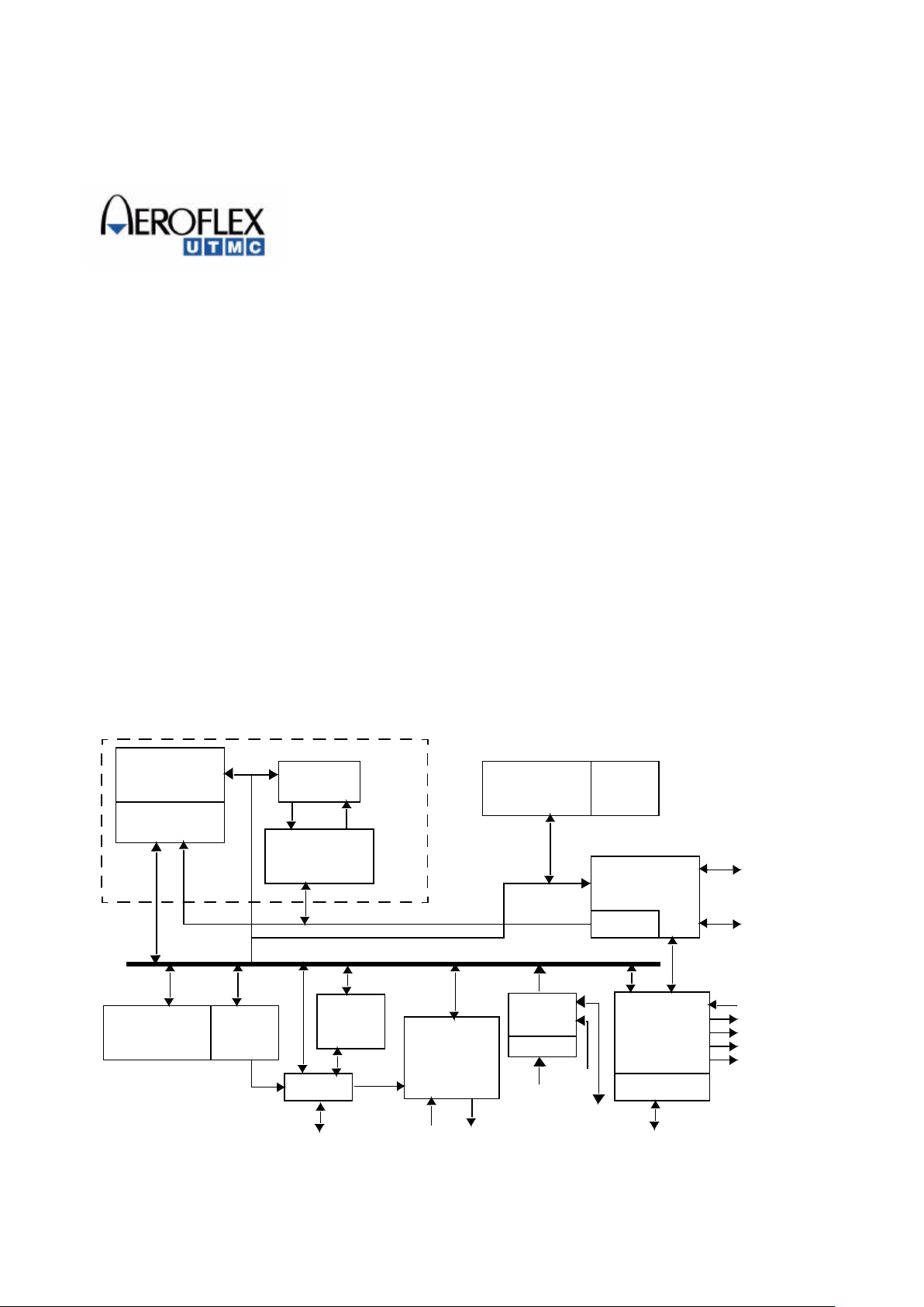
RAM
Register File
ALU
MicroCode
Engine
Interrupt
Controller
PTS
Memory
Controller
Queue
Watchdog
Timer
PWM
PORT2
Serial
Port
HSIO and
Timers
HSI HSO
Alternate
Functions
CPU
Alternate
Functions
PORT1
HOLD
HLDA
BREQ
PWM1
PWM2
Control
Signals
Address /Data Bus
Figure 1. UT80C196KDS Microcontroller
F
irstP
a
s
s
C
or
e
IP
PORT0
EXTINT
ECB0-
ECB5
FEATURES
q 20MHz 16-bit Microcontroller compatible with industry
standard’s MCS-96 ISA
- Register to Register Architecture
- 1000 Byte Register RAM
q Three 8-bit I/O Ports
q On-board Interrupt Controller
q Three Pulse-Width Modulated Outputs
q High Speed I/O
q UART Serial Port
q Dedicated Baud Rate Generator
q Software and Hardware Timers
- 16-Bit Watchdog Timer, Four 16-Bit Software Timers
- Three 16-Bit Counter/Timers
q Error detection and correction for external memory accesses
q QML Q compliant part
q Standard Microcircuit Drawing 5962-02523
INTRODUCTION
The UT80C196KDS is compatible with industry standard’s
MCS-96 instruction set. The UT80C196KDS is supported by
commercial hardware and software development tools.
The UT80C196KDS accesses instruction code and data via a
16-bit address and data bus. The 16-bit bus allows the
microcontroller to access 128K bytes of instruction/data
memory. Integrated software and hardware timers, high speed
I/O, pulse width modulation circuitry, and UART make the
UT80C196KD ideal for control type applications. The CPU’s
ALU supports byte and word adds and subtracts, 8 and 16 bit
multiplies, 32/16 and 16/8 bit divides, as well as increment,
decrement, negate, compare, and logical operations. The
UT80C196KDS’s interrupt controller prioritizes and vectors 18
interrupt events. Interrupts include normal interrupts and special
interrupts. To reduce power consumption, the microcontroller
supports software invoked idle and power down modes.
The UT80C196KDS is packaged in a 68-lead quad flatpack.
Standard Products
UT80C196KDS Microcontroller
Advanced Datasheet
April 9, 2002
2
I
N
DEVEL
O
PM
E
NT
1.0 SIGNAL DESCRIPTION
Port 0 (P0.0 - P0.7): Port 0 is an 8-bit input only port when used
in its default mode. When configured for their alternate function,
five of the bits are bi-directional EDAC check bits as shown in
Table 1.
Port 1 (P1.0 - P1.7): Port 1 is an 8-bit, quasi-bidirectional, I/O
port. All pins are quasi-bidirectional unless the alternate
function is selected per Table 2. When the pins are configured
for their alternate functions, they act as standard I/O, not quasibidirectional.
Port 2 (P2.0 - P2.7): Port 2 is an 8-bit, multifunctional, I/O port.
These pins are shared with timer 2 functions, serial data I/O and
PWM0 output, per Table 3.
AD0-AD7: The lower 8-bits of the multiplexed address/data
bus. The pins on this port are bidirectional during the data phase
of the bus cycle.
AD8-AD15: The upper 8-bits of the multiplexed address/data
bus. The pins on this port are bidirectional during the data phase
of the 16-bit bus cycle. When running in 8-bit bus width, these
pins are non-multiplexed, dedicated upper address bit outputs.
HSI: Inputs to the High Speed Input Unit. Four HSI pins are
available: HSI.0, HSI.1, HSI.2, and HSI.3. Two of these pins
(HSI.2 and HSI.3) are shared with the HSO Unit. Two of these
pins (HSI.0 and HSI.1) have alternate functions for Timer 2.
HSO: Outputs from the High Speed Output Unit. Six HSO pins
are available: HSO.0, HSO.1, HSO.2, HSO.3, HSO.4, and
HSO.5. Pins HSO.4 and HSO.5 are shared with pins HSI.2 and
HSI.3 of the HSI Unit respectively.
Table 1. Port 0 Alternate Functions
Port Pin Alternate
Name
Alternate Function
P0.0-P0.3,
P0.6
ECB0-ECB4 Error Detection & Correction
Check Bits
P0.4
P0.5
Input Port Pins
P0.7 EXTINT Setting IOC1.1=1 will allow P0.7
to be used for EXTINT (INT07)
Table 2. Port 1 Alternate Functions
Port
Pin
Alternate
Name
Alternate Function
P1.0 P1.0 I/O Pin
P1.1 P1.1 I/O Pin
P1.2 P1.2 I/O Pin
P1.3 PWM1 Setting IOC3.2=1 enables P1.3 as
the Pulse Width Modulator
(PWM1) output pin.
P1.4 PWM2 Setting IOC3.3=1 enables P1.4 as
the Pulse Width Modulator
(PWM2) output pin.
P1.5 BREQ Bus Request, output activated
when the bus controller has a
pending external memory cycle.
P1.6 HLDA Bus Hold Acknowledge, output
indicating the release of the bus.
P1.7 HOLD Bus Hold, input requesting control
of the bus.
Table 3. Port 2 Alternate Functions
Port
Pin
Alternate
Name
Alternate Function
P2.0 TXD Transmit Serial Data.
P2.1 RXD Receive Serial Data.
P2.2 EXTINT External interrupt. Clearing
IOC1.1 will allow P2.2 to be
used for EXTINT (INT07)
P2.3 T2CLK Timer 2 clock input and Serial
port baud rate generator input.
P2.4 T2RST Timer 2 Reset
P2.5 PWM0 Pulse Width Modulator
output 0
P2.6 T2UP-DN Controls the direction of the
Timer 2 counter. Logic High
equals count down. Logic low
equals count up.
P2.7 T2CAPTURE A rising edge on P2.7 causes
the value of Timer 2 to be
captured into this register, and
generates a Timer 2 Capture
interrupt (INT11).

I
N DEVE
L
OP
M
E
NT
3
1.1 Hardware Interface
1.1.1 Interfacing with External Memory
The UT80C196KDS can interface with a variety of external
memory devices. It supports either a fixed 8-bit bus width or a
dynamic 8-bit/16-bit bus width, internal READY control for
slow external memory devices, a bus-hold protocol that enables
external devices to take over the bus, and several bus-control
modes. These features provide a great deal of flexibility when
interfacing with external memory devices.
1.1.1.1 Chip Configuration Register
The Chip Configuration Register (CCR) is used to initialize the
UT80C196KDS immediately after reset. The CCR is fetched
from external address 2018H (Chip Configuration Byte) after
removal of the reset signal. The Chip Configuration Byte (CCB)
is read as either an 8-bit or 16-bit word depending on the value
of the BUSWIDTH pin. The composition of the bits in the CCR
are shown in Table 4.
There are 8 configuration bits available in the CCR. However,
bits 7 and 6 are not used by the UT80C196KDS. Bits 5 and 4
comprise the READY mode control which define internal limits
for waitstates generated by the READY pin. Bit 3 controls the
definition of the ALE/ADV pin for system memory controls
while bit 2 selects between the different write modes. Bit 1
selects whether the UT80C196KDS will use a dynamic 16-bit
bus or whether it will be locked in as an 8-bit bus. Finally, Bit
0 enables the Power Down mode and allows the user to disable
this mode for protection against inadvertent power downs.
1.1.1.2 Bus Width and Memory Configurations
The UT80C196KDS external bus can operate as either an 8-bit
or 16-bit multiplexed address/data bus (see figure 2). The value
of bit 1 in the CCR determines the bus operation. A logic low
value on CCR.1 locks the bus controller in 8-bit bus mode. If,
however, CCR.1 is a logic high, then the BUSWIDTH signal is
used to decide the width of the bus. The bus is 16 bits wide when
the BUSWIDTH signal is high, and is 8 bits when the
BUSWIDTH signal is low.
1.1.2 Reset
To reset the UT80C196KDS, hold the RESET pin low for at
least 16 state times after the power supply is within tolerance
and the oscillator has stabilized. Resets following the power-up
reset may be asserted for at least one state time, and the device
will turn on a pull-down transistor for 16 state times. This
enables the RESET signal to function as the system reset. The
reset state of the external I/O is shown in Table 9, and the register
reset values are shown in Table 8.
1.1.3 Instruction Set
The instruction set for the UT80 C196KDS is compatible with
the industry standard MCS-96 instruction set used on the
8XC196KDS.
Notes:
1.The first instruction read following reset will be from location 2080h. All other external memory can be used as instruction a nd/or data memory.
Table 4. Chip Configuration Register
Bit Function
7 N/A
6 N/A
5 IRC1 - Internal READY Mode Control
4 IRC0 - Internal READY Mode Control
3 Address Valid Strobe Select (ALE/ADV)
2 Write Strobe Mode Select (WR and BHE/WRL and WRH)
1 Dynamic Bus Width Enable
0 Enable Power Down Mode
Table 5. Memory Map
Memory Description Begin End
External Memory
1
02080H 0FFFFH
Reserved 0205EH 0207FH
PTS Vectors 02040H 0205DH
Upper Interrupt Vectors 02030H 0203FH
Reserved 02020H 0202FH
Reserved 02019H 0201FH
Chip Configuration Byte 02018H 02018H
Reserved 02014H 02017H
Lower Interrupt Vectors 02000H 02013H
External Memory 00400H 1FFFH
Internal Memory (RAM) 0001AH 003FFH
Special Function Registers 00000H 00019H

4
IN DEVELOPMENT
Table 6. Interrupt Vector Sources, Locations, and Priorities
Number Interrupt Vector Source(s)
Interrupt
Vector
Location
PTS
Vector
Location
Priority
1
(0 is the
Lowest
Priority)
Special Unimplemented
Opcode
Unimplemented Opcode 2012h N/A N/A
Special Software Trap Software Trap 2010h N/A N/A
INT 15
NMI
2
NMI 203Eh N/A 15
INT 14 HSI FIFO Full HSI FIFO Full 203Ch 205Ch 14
INT 13
EXTINT 1
2
Port 2.2 203Ah 205Ah 13
INT 12 Timer 2 Overflow Timer 2 Overflow 2038h 2058h 12
INT 11
Timer 2 Capture
2
Timer 2 Capture 2036h 2056h 11
INT 10 HSI FIFO 4 HSI FIFO
Fourth Entry
2034h 2054h 10
INT 9 Receive
RI Flag
3
2032h 2052h 9
INT 8 Transmit
TI Flag
3
2030h 2050h 8
INT 7
EXTINT
2
Port 2.2 or Port 0.7 200Eh 204Eh 7
INT 6 Serial Port RI Flag and
TI Flag
4
200Ch 204Ch 6
INT 5 Software Timer Software Timer 0-3
Timer 2 Reset
200Ah 204Ah 5
INT 4
HSI.0
2
HSI.0 Pin 2008h 2048h 4
INT 3 High Speed
Outputs
Events on HSO.0 thru
HSO.5 Lines
2006h 2046h 3
INT 2 HSI Data Available HSI FIFO Full or
HSI Holding Reg.
Loaded
2004h 2044h 2
INT 1 EDAC Bit Error Single Bit Error
Single Bit Error OVF
Double Bit Error
2002h 2042h 1
INT 0 Timer Overflow Timer 1 or Timer 2 2000h 2040h 0
All of the previous maskable interrupts can be assigned to the PTS.
Any PTS interrupt has priority over all other maskable interrupts.

I
N DEVE
L
OP
M
E
NT
5
Notes:
1. The Unimplemented Opcode and Software Trap interrupts are not prioritized. The Interrupt Controller immediately services these interrupts when they are
asserted. NMI has the highest priority of all prioritized interrupts. Any PTS interrupt has priority over lower priority interru pts, and over all other maskable
interrupts. The standard maskable interrupts are serviced according to their priority number with INT0 has the lowest priority of all interrupts.
2. These interrupts can be configured to function as independent, external interrupts.
3. If the Serial interrupt is masked and the Receive and Transmit interrupts are enabled, the RI flag and TI flag generate separate Receive and Transmit interrupts.
4. If the Receive and Transmit interrupts are masked and the Serial interrupt is enabled, both RI flag and TI flag generate a Serial Port interrupt.

6
IN DEVELOPMENT
Notes:
1. For some functions that share a register address in HWindow0, the opposite access type (read/write) is available in HWindow 15 if
indicated by the three asterisks (***).
2. These registers are not available in the industry standard 8XC196KDS. Therefore, industry standard development software will not recognize these
mnemonics, and you will only be able to access them via their physical addresses.
Table 7. SFR Memory Mapping
Address HWin 0 Read HWin 0 Write HWin 1
HWin 15
1
019H Stack Pntr (hi) Stack Pntr (hi) Stack Pntr (hi) Stack Pntr (hi)
018H Stack Pntr (lo) Stack Pntr (lo) Stack Pntr (lo) Stack Pntr (lo)
017H IOS2 PWM0_CTRL PWM2_CTRL ***
016H IOS1 IOC1 PWM1_CTRL ***
015H IOS0 IOC0
EDAC-CS
2
***
014H WSR WSR WSR WSR
013H INT_MASK1 INT_MASK1 INT_MASK1 INT_MASK1
012H INT_PEND1 INT_PEND1 INT_PEND1 INT_PEND1
011H SP_STAT SP_CON RESERVED ***
010H PORT 2 PORT 2 RESERVED
PSW
2
00FH PORT 1 PORT 1
Timer 3(hi)
2
RESERVED
00EH PORT 0 BAUD RATE
Timer 3(lo)
2
RESERVED
00DH Timer 2 (hi) Timer 2 (hi)
WDT-SCALE
2
T2CAPTURE (hi)
00CH Timer 2 (lo) Timer 2 (lo) IOC3 T2CAPTURE (lo)
00BH Timer 1 (hi) IOC2
INT_PRI(hi)
2
***
00AH Timer 1 (lo) Watchdog
INT_PRI(lo)
2
***
009H INT_PEND INT_PEND INT_PEND INT_PEND
008H INT_MASK INT_MASK INT_MASK INT_MASK
007H SBUF (RX) SBUF (TX) PTSSRV (hi) ***
006H HSI_status HSO_command PTSSRV (lo) ***
005H HSI_time(hi) HSO_time (hi) PTSSEL (hi) ***
004H HSI_time (lo) HSO_time (lo) PTSSEL (lo) ***
003H RESERVED HSI_mode RESERVED ***
002H RESERVED RESERVED RESERVED RESERVED
001H Zero_reg (hi) Zero_reg (hi) Zero-reg (hi) Zero_reg (hi)
000H Zero_reg (lo) Zero_reg (lo) Zero_reg (lo) Zero_reg (lo)

I
N DEVE
L
OP
M
E
NT
7
Table 8: Special Function Register Reset Values
Internal Register Binary Reset State
Hexadecimal Reset
Value
Stack Pointer (SP) XXXX XXXX XXXX XXXX XXXX
I/O Status Register 2 (IOS2) 0000 0000 00
I/O Status Register 1 (IOS1) 0000 0000 00
I/O Status Register 0 (IOS0) 0000 0000 00
Window Select Register (WSR) 0000 0000 00
Interrupt Mask Register 1 (INT_MASK1) 0000 0000 00
Interrupt Pending Register 1
(INT_PEND1)
0000 0000 00
Serial Port Status Register (SP_STAT) 0000 1011 0B
Port 2 Register (PORT2) 110X XXX1 XX
Port 1 Register (PORT1) 1111 1111 FF
Port 0 Register (PORT0) XXXX XXXX XX
Timer 2 Value Register (TIMER2) 0000 0000 0000 0000 0000
Timer 1 Value Register (TIMER1) 0000 0000 0000 0000 0000
Interrupt Pending Register (INT_PEND) 0000 0000 00
Interrupt Mask Register (INT_MASK) 0000 0000 00
Receive Serial Port Register (SBUF
(RX))
0000 0000 00
HSI Status Register (HSI_status) X0X0 X0X0 XX
HSI Time Register (HSI_time) XXXX XXXX XXXX XXXX XXXX
Zero Register (ZERO_REG) 0000 0000 0000 0000 0000
PWM0 Control Register (PWM0_CTRL) 0000 0000 00
I/O Control Register 1 (IOC1) 0010 0001 21
I/O Control Register 0 (IOC0) 0000 00X0 0X
Serial Port Control Register (SP_CON) 0000 1011 0B
Baud Rate Register (BAUD_RATE) 0000 0000 0000 0001 0001
I/O Control Register 2 (IOC2) X00X X000 XX
Watch Dog Timer Register (WATCH-
DOG)
0000 0000 00

8
IN DEVELOPMENT
Transmit Serial Port Buffer (SBUF (TX)) 0000 0000 00
HSO Command Register
(HSO_command)
0000 0000 00
HSO Time Register (HSO_time) 0000 0000 0000 0000 0000
HSI Mode Register (HSI_mode) 1111 1111 FF
PWM2 Control Register (PWM2_CTRL) 0000 0000 00
PWM1 Control Register (PWM1_CTRL) 0000 0000 00
EDAC Control and Status Register
(EDAC_CS)
0000 0000 00
Timer 3 Value Register (TIMER3) 0000 0000 0000 0000 0000
Watchdog Timer Prescaler
(WDT_SCALE)
0000 0000 00
I/O Control Register 3 (IOC3) 1111 0000 F0
Interrupt Priority Register (INT_PRI) 0000 0000 00
PTS Service Register (PTSSRV) 0000 0000 0000 0000 0000
PTS Select Register (PTSSEL) 0000 0000 0000 0000 0000
Timer 2 Capture Register
(T2CAPTURE)
0000 0000 0000 0000 0000
Program Counter (PC) 0010 0000 1000 0000 2080
Chip Configuration Register (CCR) XX10 1111 XF
Table 8: Special Function Register Reset Values
Internal Register Binary Reset State
Hexadecimal Reset
Value

I
N DEVE
L
OP
M
E
NT
9
Table 9: External I/O Reset State
External I/O I/O Function After Reset
I/O State During
Reset
I/O State After Reset
Address/Data Bus (AD15:0) Address/Data Bus Pulled High Driven Output
ALE
ADV
ALE Pulled High Driven Output
RD RD Pulled High Driven Output
WR
WRL
WR Pulled High Driven Output
Port 0 (P0.0-P0.3; P0.6)
ECB(4:0)
[P0.0-P0.3; P0.6] and
ECB(4:0)
Undefined Inputs
1
Undefined I/O
1,2
Port 0 (P0.4 and P0.5) P0.4 and P0.5
Undefined Inputs
1
Undefined Inputs
1
Port 0 (P0.7)
EXTINT
P0.7
Undefined Input
1
Undefined Input
1
NMI NMI Pulled Down Pulled Down
HSI.0
T2RST
HSI.0
Disabled Input
1
Disabled Input
1
HSI.1
T2CLK
HSI.1
Disabled Input
1
Disabled Input
1
HSI.2/HSO.4 Undefined
Disabled I/O
1
Disabled I/O
1
HSI.3/HSO.5 Undefined
Disabled I/O
1
Disabled I/O
1
HSO.0 through HSO.3 HSO.0-HSO.3 Pulled Down Driven Low
Outputs
Port 1 (P1.0-P1.7)
PWM1; PWM2;
BREQ; HLDA; HOLD
P1.0-P1.7 Pulled Up Pulled Up
Port 2 (P2.0)
TXD
TXD Pulled Up Driven High
Output
Port 2 (P2.1)
RXD
RXD
Undefined Input
1
Undefined Input
1
Port 2 (P2.2)
EXTINT
P2.2 and EXTINT
Undefined Input
1
Undefined Input
1
Port 2 (P2.3)
T2CLK
P2.3 and T2CLK
Undefined Input
1
Undefined Input
1
Port 2 (P2.4)
T2RST
P2.4
Undefined Input
1
Undefined Input
1
10
IN DEVELOPMENT
Notes:
1. These pins must not be left floating. Input voltages must not exceed VDD during power-up.
2. Do not directly tie these pins to V
DD
or GND; if EDACEN goes low, they may be driven by the UT80C196KDS and bus contention may occur.
Port 2 (P2.5)
PWM0
PWM0 Pulled Down Driven Low Output
Port 2 (P2.6)
T2UP-DN
P2.6 Pulled Up Pulled Up
Port 2 (P2.7)
T2CAPTURE
P2.7 and T2CAPTURE Pulled Up Pulled Up
EDACEN EDACEN
Undefined Input
1
Undefined Input
1
ECB5/ADV_RD_ WR ECB5/ADV_RD_WR
Undefined I/O
1
Undefined I/O
1,2
READY READY
Undefined Input
1
Undefined Input
1
BUSWIDTH BUSWIDTH
Undefined Input
1
Undefined Input
1
BHE
WRH
BHE Pulled Up Driven Output
CLKOUT CLKOUT Driven Output Driven Output
INST INST Pulled Down Driven Output
RESET RESET Pulled Low by
System
Pulled Up
Table 9: External I/O Reset State
External I/O I/O Function After Reset
I/O State During
Reset
I/O State After Reset
I
N DEVE
L
OP
M
E
NT
11
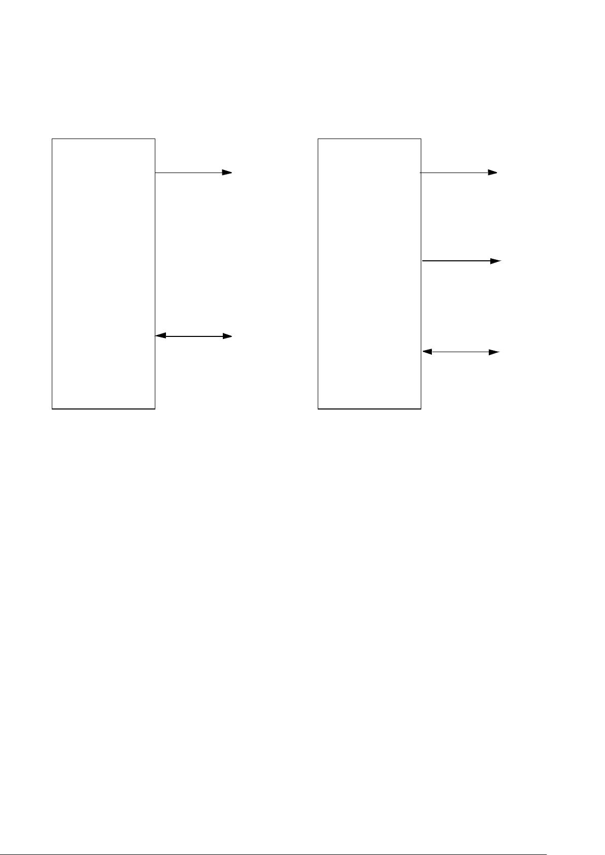
UT80C196KDS UT80C196KDS
Bus Control
16-Bit
Multiplexed
Address/Data
8-Bit
Multiplexed
Address/Data
8-Bit
Latched
Address High
Bus Control
AD0-AD15
AD0-AD7
AD8-AD15
16-Bit Bus 8-Bit Bus
Figure 2. Bus Width Options
12
IN DEVELOPMENT
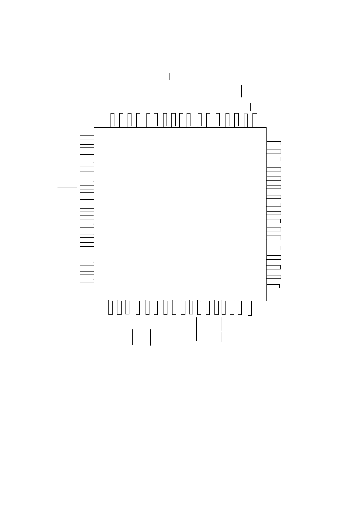
60
59
58
57
56
55
54
53
52
51
50
49
48
47
46
45
44
27
28
29
30
31
32
33
34
35
36
37
38
39
40
41
42
43
9
8
7
6
5
4
3
2
1
68
67
66
65
64
63
62
61
UT80C196KDS
TOP VIEW
Figure 3. 68-pin Quad Flatpack Package
AD0
AD1
AD2
AD3
AD4
AD5
AD6
AD7
AD8
AD9
AD10
AD11
AD12
AD13
AD14
AD15
P2.3/T2CLK
HSI.3/HSO.5
HS0.0
HS0.1
BR EQ/P1.5
HLDA/P1.6
HOLD/P1.7
T2UP-DN/P2.6
HS0.2
HS0.3
V
SS
EDACEN
T2CAPTURE/P2.7
PWM0/P2.5
WR/WRL
BHE/WRH
T2RST/P2.4
READY
P0.7/EXTINT
P0.6/ECB0
P0.2/ECB1
P0.0/ECB2
P0.1/ECB3
P0.3/ECB4
NMI
ECB5/ADV _RD_WR
VDDVSSXTAL1
VSSCLKOUT
BUSWIDTH
INST
ALE/ADV
RD
10
11
12
13
14
15
16
17
18
19
20
21
22
23
24
25
26
P0.5
P0.4
V
SS
V
DD
V
SS
EXTINT/P2.2
RESET
RXD/P2.1
TXD/P2.0
P1.0
P1.1
P1.2
PWM1/P1.3
PWM2/P1.4
T2RST/HSI.0
T2CLK/HSI.1
HSI.2/HS0.4

I
N DEVE
L
OP
M
E
NT
13
Legend for I/O fields:
TO = TTL compatible output
TI = TTL compatible input
CI = CMOS only input
TUO = TTL compatible output
(internally pulled high)
TDO = TTL compatible output
(internally pulled low)
TUI = TTL compatible input
(internally pulled high)
TDI = TTL compatible input
(internally pulled low)
TB = TTL compatible bidirectional
TUQ = TTL compatible quasi-bidirectional
(internally pulled high)
TUB = TTL compatible bidirectional
(internally pulled high)
TUBS = TTL compatible bidirectional Schmitt
Trigger (internally pulled high)
PWR = +5V (VDD)
GND = OV (VSS)
Table 10: 68-lead Flat Pack Pin Descriptions
QFP Pin# I/O Name Active Description
1 PWR V
DD
--- Digital supply voltage (+5V). There are 2 VDD pins, both of
which must be connected.
2 TO
ADV_RD_WR
--- Advanced Read and Write. This pin has multiplexed functionality: coincident with the Address/Data bus multiplexing. When
address information is output on the AD pins, ADV_RD_ WR is
output. When data information is on the AD pins, ECB5 is an I/
O. ADV_RD_WR is output high for an external memory read
cycle, and low for an external memory write cycle.
TB
ECB5
1
-- EDAC Check Bit 5. Asserting the EDACEN pin will cause the
error detection and correction engine to pass the EDAC Check
Bit 5 through pin 2 of the UT80C196KDS during the data phase
of an external memory cycle.
3 TDI NMI High Non-Maskable Interrupt. A positive transition causes a vector
through the NMI interrupt at location 203Eh. Assert NMI for at
least 1 state time to guarantee acknowledgment by the interrupt
controller.
4 TI P0.3 --- Port 0 Pin 3. An input only port pin that is read at location 0Eh
in HWindow 0.
TB
ECB4
1
--- EDAC Check Bit 4. Asserting the EDACEN pin will cause the
error detection and correction engine to pass the EDAC Check
Bit 4 through pin 4 of the UT80C196KDS.
5 TI P0.1 --- Port 0 Pin 1. An input only port pin that is read at location 0Eh
in HWindow 0.
TB
ECB3
1
--- EDAC Check Bit 3. Asserting the EDACEN pin will cause the
error detection and correction engine to pass the EDAC Check
Bit 3 through pin 5 of the UT80C196KDS.
 Loading...