

Aeroflex UTMC UT54ACTS273, UT54ACS273 Datasheet
189 RadHard MSI Logic
UT54ACS273/UT54ACTS273
Radiation-Hardened
Octal D-Flip-Flops with Clear
FEATURES
Contains eight flip-flops with single-rail outputs
Buffered clock and direct clear inputs
Individual data input to each flip-flop
Applications include:
- Buffer/storage registers, shift registers, and pattern
generators
radiation-hardened CMOS
- Latchup immune
High speed
Low power consumption
Single 5 volt supply
Available QML Q or V processes
Flexible package
- 20-pin DIP
- 20-lead flatpack
DESCRIPTION
The UT54ACS273 and the UT54ACTS273 are positive-edgetriggered D-type flip-flops with a direct clear input.
Information at the D inputs meeting the setup time requirements
is transferred to the Q outputs on the positive-going edge of the
clock pulse. When the clock input is at either the high or low
level, the D input signal has no effect at the output.
The devices are characterized over full military temperature
range of -55 C to +125 C.
FUNCTION TABLE
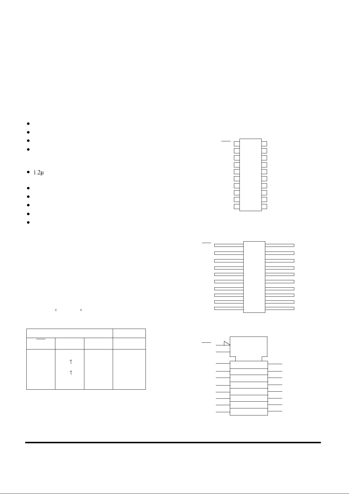
PINOUTS
20-Pin DIP
Top View
20-Lead Flatpack
Top View
LOGIC SYMBOL
INPUTS OUTPUTS
CLR CLK D
x
Q
x
L X X L
H
H
H
L
H
L
X
H
L
No change
1
2
3
4
5
7
6
20
19
18
17
16
14
15
CLR
1Q
1D
2D
2Q
3Q
3D
V
DD
8Q
8D
7D
7Q
6D
8
134D 5D
6Q
9
124Q
5Q
10
11V
SS
CLK
1
2
3
4
5
7
6
20
19
18
17
16
14
15
CLR
1Q
1D
2D
2Q
3Q
3D
V
DD
8Q
8D
7D
7Q
6D
8
13
4D
5D
6Q
9
12
4Q
5Q
10
11
V
SS
CLK
(1)
CLR
(11)
CLK
C1
R
(3)
1D
(4)
2D
(2)
1Q
(6)
3Q
(9)
4Q
(12)
5Q
(15)
6Q
(16)
7Q
(19)
8Q
1D
(7)
3D
(8)
4D
(13)
5D
(14)
6D
(17)
7D
(18)
8D
(5)
2Q
Note:
1. Logic symbol in accordance with ANSI/IEEE standard 91-1984
and IEC Publication 617-12.
RadHard MSI Logic 190
UT54ACS273/UT54ACTS273
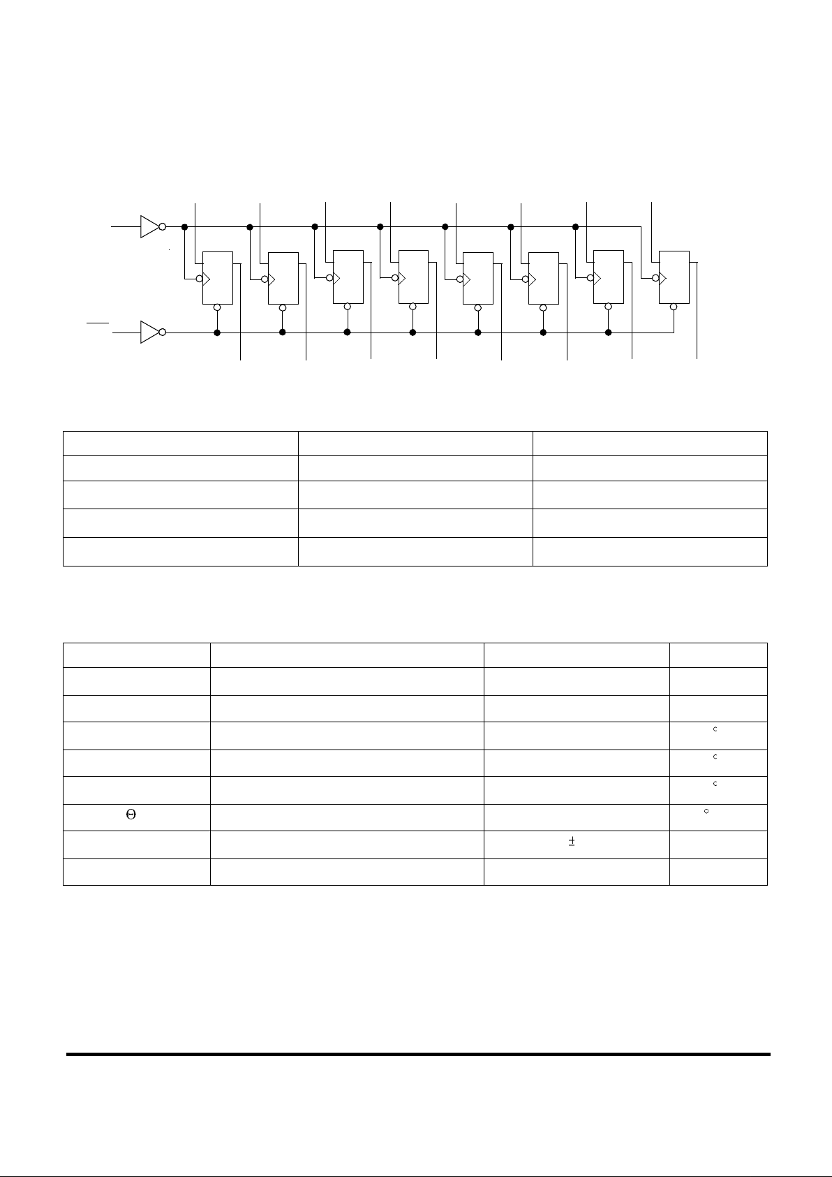
LOGIC DIAGRAM
RADIATION HARDNESS SPECIFICATIONS
1
Notes:
1. Logic will not latchup during radiation exposure within the limits defined in the table.
2. Device storage elements are immune to SEU affects.
ABSOLUTE MAXIMUM RATINGS
Note:
1. Stresses outside the listed absolute maximum ratings may cause permanent damage to the device. This is a stress rating only, functional operation of the device
at these or any other conditions beyond limits indicated in the operational sections is not recommended. Exposure to absolute maximum rating conditions for
extended periods may affect device reliability.
PARAMETER LIMIT UNITS
Total Dose 1.0E6 rads(Si)
SEU Threshold
2
80
MeV-cm2/mg
SEL Threshold 120
MeV-cm2/mg
Neutron Fluence 1.0E14
n/cm
2
1D
(3)
1Q
(2)
2D
(4)
2Q
(5)
3D
(7)
3Q
(6)
4D
(8)
4Q
(9)
5D
(13)
5Q
(12)
6D
(14)
6Q
(15)
7D
(17)
7Q
(16)
8D
(18)
8Q
(19)
C
(11)
(1)
CLR
CLK
D
R
C
D
R
C
D
R
C
D
R
C
D
R
C
D
R
C
D
R
C
D
R
SYMBOL PARAMETER LIMIT UNITS
V
DD
Supply voltage -0.3 to 7.0 V
V
I/O
Voltage any pin -.3 to VDD +.3 V
T
STG
Storage Temperature range -65 to +150 C
T
J
Maximum junction temperature +175 C
T
LS
Lead temperature (soldering 5 seconds) +300 C
JC
Thermal resistance junction to case 20 C/W
I
I
DC input current 10 mA
P
D
Maximum power dissipation 1 W
 Loading...