

Aeroflex UTMC UT54ACTS164, UT54ACS164 Datasheet
107 RadHard MSI Logic
UT54ACS164/UT54ACTS164
Radiation-Hardened
8-Bit Shift Registers
FEATURES
AND-gated (enable/disable) serial inputs
Fully buffered clock and serial inputs
Direct clear
radiation-hardened CMOS
- Latchup immune
High speed
Low power consumption
Single 5 volt supply
Available QML Q or V processes
Flexible package
- 14-pin DIP
- 14-lead flatpack
DESCRIPTION
The UT54ACS164 and the UT54ACTS164 are 8-bit shift registers which feature AND-gated serial inputs and an asynchronous clear. The gated serial inputs (A and B) permit complete
control over incoming data. A low at either input inhibits entry
of new data and resets the first flip-flop to the low level at the
next clock pulse. A high-level at both serial inputs sets the first
flip-flop to the high level at the next clock pulse. Data at the
serial inputs may be changed while the clock is high or low,
providing the minimum setup time requirements are met.
Clocking occurs on the low-to-high-level transition of the clock
input.
The devices are characterized over full military temperature
range of -55 C to +125 C.
FUNCTION TABLE
Notes:
1. QA0, QB0, QH0 = the level of QA, QB or QH, respectively, before the indicated
steady-state input conditions were established.
2. QAn and QGn = the level of QA or QG before the most recent transition of
the clock; indicates a one-bit shift.
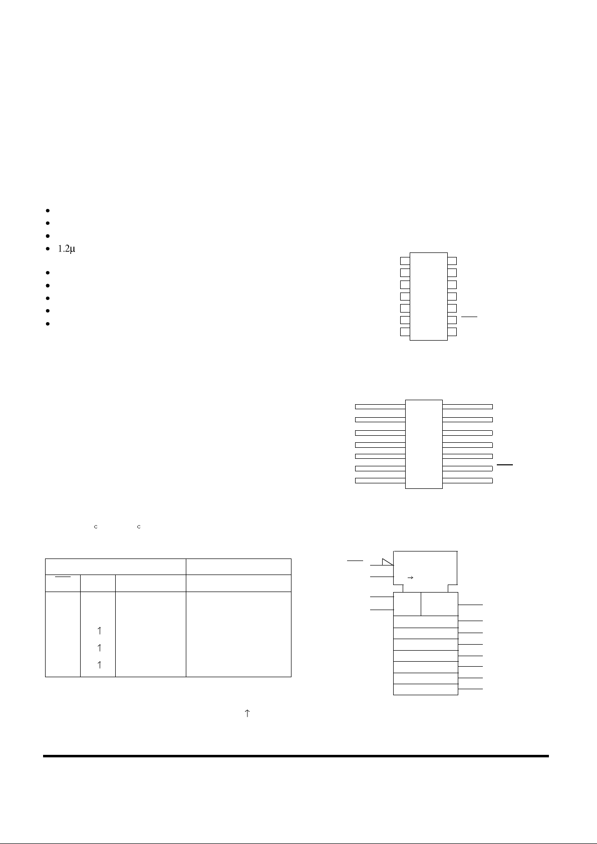
PINOUTS
14-Pin DIP
Top View
14-Lead Flatpack
Top View
LOGIC SYMBOL
INPUTS OUTPUTS
CLR CLK A B Q
A
Q
B ... QH
L X X X L L L
H L X X Q
A0
Q
B0
Q
H0
H H H H Q
An
Q
Gn
H L X L Q
An
Q
Gn
H X L L Q
An
Q
Gn
1
2
3
4
5
7
6
14
13
12
11
10
8
9
A
B
Q
A
Q
B
Q
C
Q
D
V
SS
V
DD
Q
H
Q
G
Q
F
Q
E
CLR
CLK
1
2
3
4
5
7
6
14
13
12
11
10
8
9
V
DD
Q
H
Q
G
Q
F
Q
E
CLR
CLK
A
B
Q
A
Q
B
Q
C
Q
D
V
SS
(9)
CLR
(8)
CLK
R
1D
Note:
1. Logic symbol in accordance with ANSI/IEEE Std 91-1984 and
IEC Publication 617-12.
(1)
A
(2)
B
(3)
Q
A
SRG8
&
(4)
Q
B
(5)
Q
C
(6)
Q
D
(10)
Q
E
(11)
Q
F
(12)
Q
G
(13)
Q
H
C1/
RadHard MSI Logic 108
UT54ACS164/UT54ACTS164
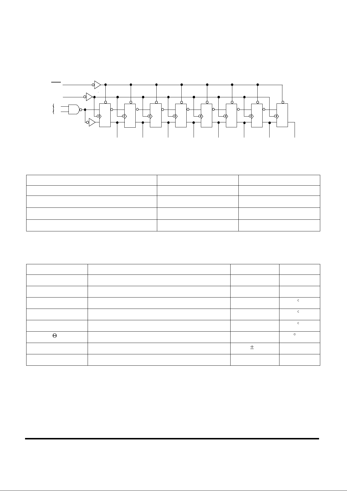
LOGIC DIAGRAM
RADIATION HARDNESS SPECIFICATIONS
1
Notes:
1. Logic will not latchup during radiation exposure within the limits defined in the table.
2. Device storage elements are immune to SEU affects.
ABSOLUTE MAXIMUM RATINGS
Note:
1. Stresses outside the listed absolute maximum ratings may cause permanent damage to the device. This is a stress rating only, functional operation of the device
at these or any other conditions beyond limits indicated in the operational sections is not recommended. Exposure to absolute maximum rating conditions for
extended periods may affect device reliability.
PARAMETER LIMIT UNITS
Total Dose 1.0E6 rads(Si)
SEU Threshold
2
80
MeV-cm2/mg
SEL Threshold 120
MeV-cm2/mg
Neutron Fluence 1.0E14
n/cm
2
Q
A
(8)
CLK
K K
R
S
K
R
S
K
R
S
K
R
S
K
R
S
K
R
S
K
R
S
Q
B
Q
C
Q
D
Q
E
Q
F
Q
G
Q
H
CLR
(9)
(2)
(1)
A
B
SERIAL
R
S
C
C
C C C
C
C
C
(3)
(4) (5) (6) (10) (11) (12) (13)
SYMBOL PARAMETER LIMIT UNITS
V
DD
Supply voltage -0.3 to 7.0 V
V
I/O
Voltage any pin -.3 to VDD +.3 V
T
STG
Storage Temperature range -65 to +150 C
T
J
Maximum junction temperature +175 C
T
LS
Lead temperature (soldering 5 seconds) +300 C
JC
Thermal resistance junction to case 20 C/W
I
I
DC input current 10 mA
P
D
Maximum power dissipation 1 W
 Loading...