

Aeroflex UTMC UT54ACTS109, UT54ACS109 Datasheet
UT54ACS109/UT54ACTS109
Radiation-Hardened
Dual J-K Flip-Flops
FEATURES
• radiation-hardened CMOS
- Latchup immune
• High speed
• Low power consumption
• Single 5 volt supply
• Available QML Q or V processes
• Flexible package
- 16-pin DIP
- 16-lead flatpack
DESCRIPTION
The UT54ACS109 and the UT54ACTS109 are dual J-K positive triggered flip-flops. A low level at the preset or clear inputs
sets or resets the outputs regardless of the other input levels.
When preset and clear are inactive (high), data at the J and K
input meeting the setup time requirements are transferred to the
outputs on the positive-going edge of the clock pulse. Following
the hold time interval, data at the J and K input can be changed
without affecting the levels at the outputs. The flip-flops can
perform as toggle flip-flops by grounding K and tying J high.
They also can perform as D flip-flops if J and K are tied together.
The devices are characterized over full military temperature
range of -55 C to +125 C.
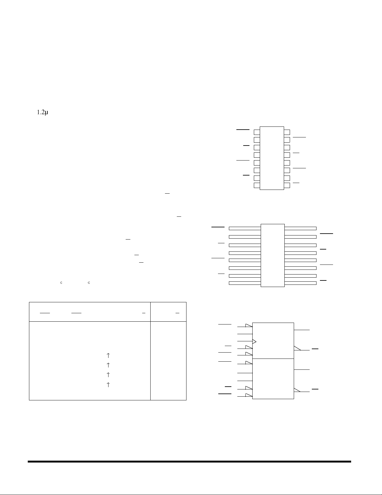
FUNCTION TABLE
PINOUTS
CLR1
J1
K1
CLK1
PRE1
Q1
Q1
V
SS
16-Pin DIP
Top View
SS
1
2
J
3
4
5
6
7
8 9
CLR1
K1
CLK1
PRE1
Q1
Q1
V
16-Lead Flatpack
Top View
1
2
3
4
5
6
7
8 9
16
15
14
13
12
11
10
16
15
14
13
12
11
10
V
DD
CLR2
J2
K2
CLK2
PRE2
Q2
Q2
V
DD
CLR2
J2
K2
CLK2
PRE2
Q2
Q2
INPUTS OUTPUT
PRE CLR CLK J K Q Q
L H X X X H L
H L X X X L H
L L X X X
H H L L L H
H H H L Toggle
H H L H No Change
H H H H H L
H H L X X No Change
Note:
1. The output levels in this configuration are not guaranteed to meet the minimum levels for VOH if the lows at preset and clear are near V
addition, this configuration is nonstable; that is, it will not persist when either
preset or clear returns to its inactive (high) level.
1
H
maximum. In
IL
H
LOGIC SYMBOL
1
Note:
1. Logic symbol in accordance with ANSI/IEEE standard 91-1984 and
IEC Publication 617-12.
PRE1
J1
CLK1
K1
CLR1
PRE2
J2
CLK2
K2
CLR2
(5)
(2)
(4)
(3)
(1)
(11)
(14)
(12)
(13)
(15)
S
J1
K1
R
C1
(6)
(7)
(10)
(9)
Q1
Q1
Q2
Q2
61 RadHard MSI Logic
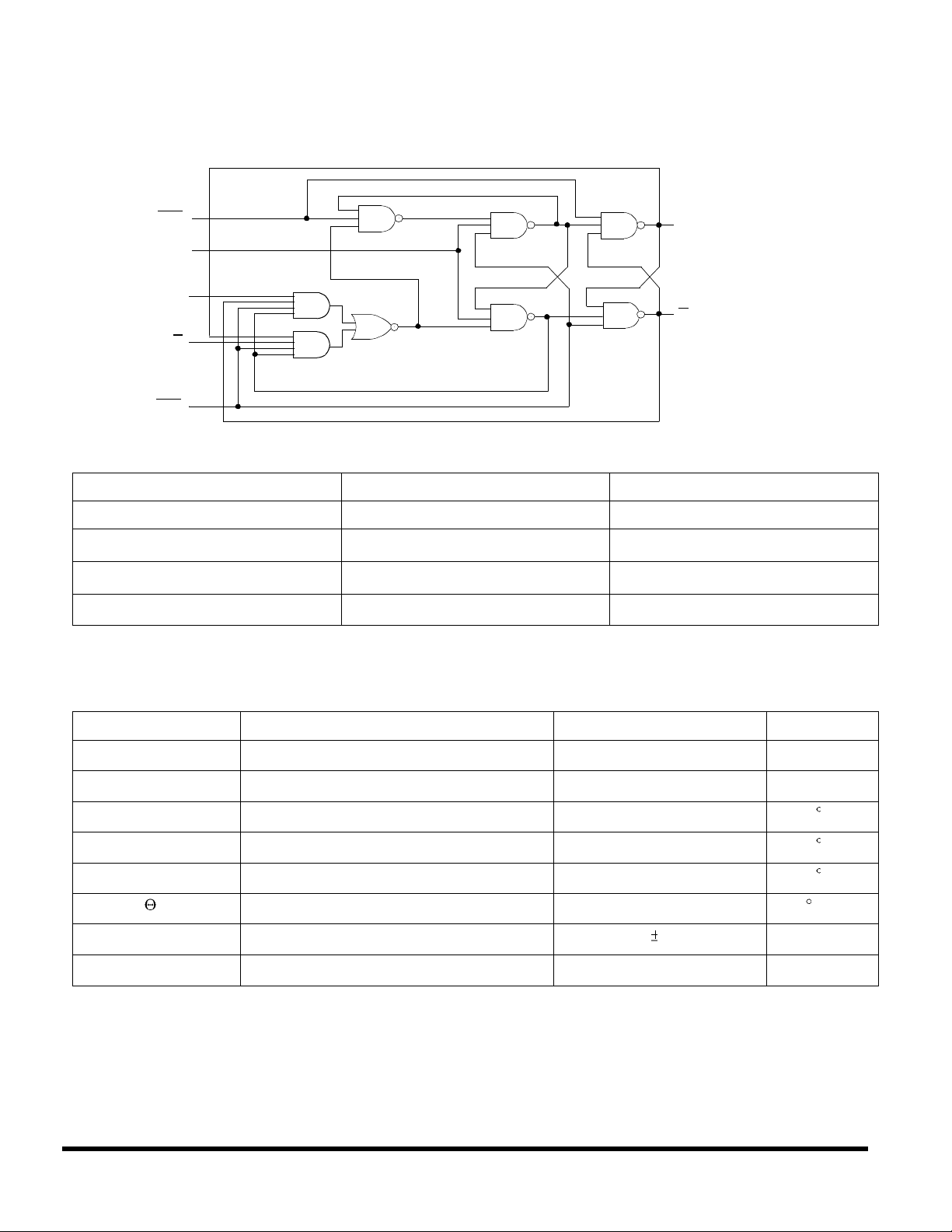
LOGIC DIAGRAM
UT54ACS109/UT54ACTS109
PRE
CLK
J
K
CLR
RADIATION HARDNESS SPECIFICATIONS
1
PARAMETER LIMIT UNITS
Total Dose 1.0E6 rads(Si)
SEU Threshold
2
80
SEL Threshold 120
Neutron Fluence 1.0E14
Notes:
1. Logic will not latchup during radiation exposure within the limits defined in the table.
2. Device storage elements are immune to SEU affects.
ABSOLUTE MAXIMUM RATINGS
Q
Q
MeV-cm2/mg
MeV-cm2/mg
n/cm
2
SYMBOL PARAMETER LIMIT UNITS
V
DD
V
I/O
T
STG
T
J
T
LS
JC
I
I
P
D
Note:
1. Stresses outside the listed absolute maximum ratings may cause permanent damage to the device. This is a stress rating only, functional operation of the device
at these or any other conditions beyond limits indicated in the operational sections is not recommended. Exposure to absolute maximum rating conditions for
extended periods may affect device reliability.
Maximum junction temperature +175 C
Lead temperature (soldering 5 seconds) +300 C
Thermal resistance junction to case 20 C/W
Supply voltage -0.3 to 7.0 V
Voltage any pin -.3 to VDD +.3 V
Storage Temperature range -65 to +150 C
DC input current 10 mA
Maximum power dissipation 1 W
RadHard MSI Logic 62
 Loading...