

Aeroflex UTMC UT1553RTMP Datasheet
RTMP-1
UT1553 Remote Terminal Multi-Protocol
FEATURES
p Complete MIL-STD-1553 Remote Terminal Interface
p Mode selectable to comply with either MIL-STD-
1553A or MIL-STD-1553B bus protocol
p Mil-STD-1773 compatible
p Remote terminal operation is certified by ASD/
ENASC (SEAFAC)
p Implements all dual-redundant Remote Terminal mode
codes and operational functions including broadcast
commands
p Provides handshake control for quad-redundant
systems
p Data pointers permit programmable memory mapping
for 1553 data over the entire 64K host memory space
p Provides all handshaking signals for a DMA interface
p Stores 1553 command word and time-tag information
with all incoming data for enhanced data management
p Three-state address bus, databus, and control signals
simplify DMA operations
p Supports end-of-command activity and data bus error
interrupts
p Self-test capability
p Available as a gate array macrocell
p Available in 84-pin pingrid array, 84-lead leadless chip
carrier, or 84-lead flatpack packages
p Standard Microcircuit Drawing 5962-88645 available
- QML Q compliant
INTRODUCTION
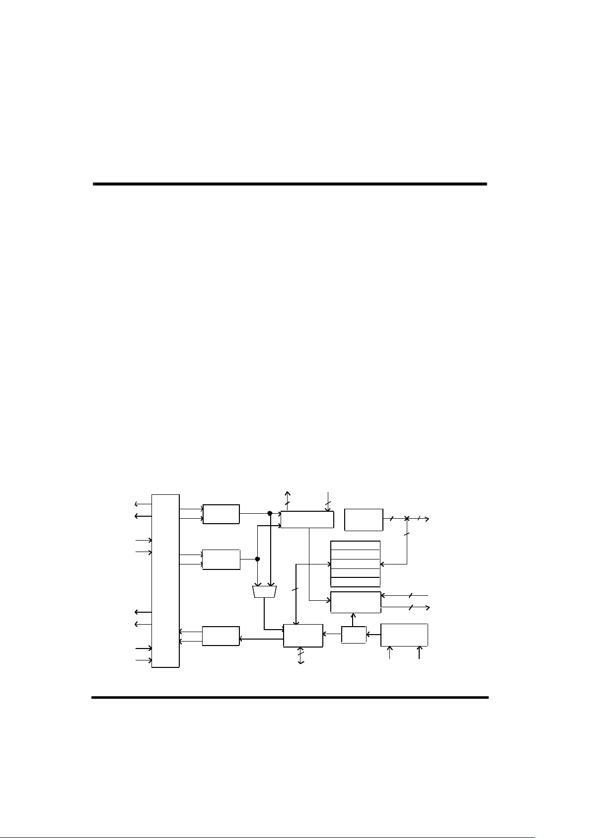
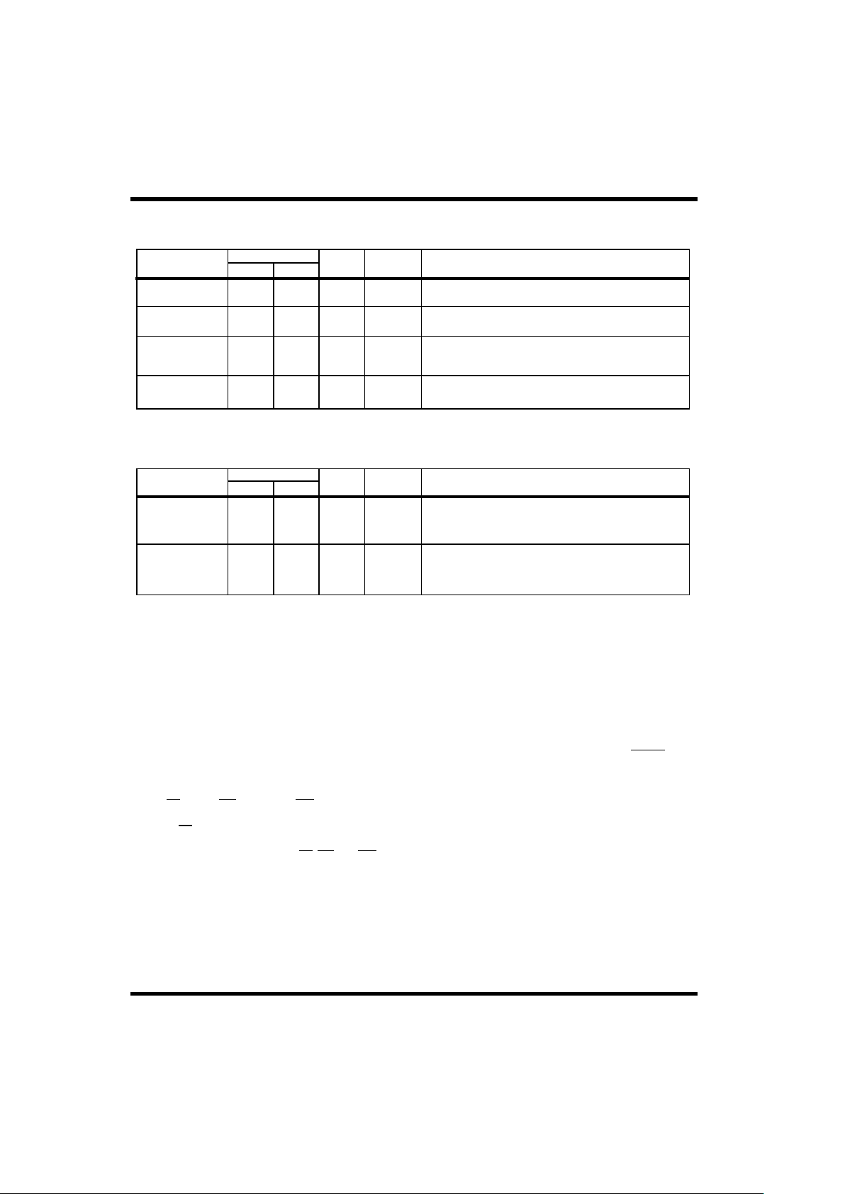
The UT1553 RTMP (figures 1 and 4) is a monolithic,
CMOS, VLSI integrated circuit that meets all requirements
for a dual-redundant MIL-STD-1553 Remote Terminal
interface. The RTMP’s advanced design supports both
MIL-STD-1553A and MIL-STD-1553B serial data bus
protocols, including differences in the status word response
time and bit definitions, providing the system designer a
single-chip solution to most Remote Terminal interface
requirements.
The UT1553 RTMP provides all requisite 1553 protocol and
data handling, 1553 message error checking, DMA
handshake and control signals, and comprehensive self-test
capabilities. The RTMP’s pointer-based, programmable
memory-mapping architecture permits the host to map 1553
message data anywhere in the 64K memory space. This
advanced memory mapping, along with the RTMP’s control
and status functions, minimize the host system’s 1553
interface overhead.
The UT1553 RTMP is a member of UTMC’s complete
family of high-reliability monolithic MIL-STD-1553
interface products.
16
55
SUBADDRESS ADDRESS
TERMINALMODE CODE/
3
16
16
16
9
13
OUTPUTS
CONTROL
INPUTS
CONTROL
ADDRESS
MEMORY
CONTROL
ADDRESS
MEMORY
DATA
TIME TAG
CONTROL
BASE PTR
STATUS
LAST CMD
LOGIC
CONTROL
AND ERROR
12MHz
RESET
MASTER
LOGIC
RESET
CLOCK AND
TIMER
LOGIC
TRANSFER
LOGIC
DATA
COMMAND
RECOGNITION
MUX
OUT
IN
A
OUT
IN
B
DECODER
DECODER
ENCODER
CHANNEL
CHANNEL
OUTPUT MULTIPLEXING AND
SELF-TEST WRAPAROUNDLOGIC
Figure 1. UT1553 RTMP Functional Block Diagram

RTMP-2
Table of Contents
1.0 FUNCTIONAL DESCRIPTION . . . . . . . . . . . . . . . . . . . . . . . . . . . . . . . . . . . . . . . .3
2.0 PIN IDENTIFICATION AND DESCRIPTION. . . . . . . . . . . . . . . . . . . . . . . . . . . .5
3.0 REMOTE TERMINAL ARCHITECTURE. . . . . . . . . . . . . . . . . . . . . . . . . . . . . .11
3.1 Internal Registers . . . . . . . . . . . . . . . . . . . . . . . . . . . . . . . . . . . . . . . . . . . . . . .11
3.2 Read/Write Register . . . . . . . . . . . . . . . . . . . . . . . . . . . . . . . . . . . . . . . . . . . . .11
3.3 Time Tag Data Register . . . . . . . . . . . . . . . . . . . . . . . . . . . . . . . . . . . . . . . . . .11
3.4 Control Register . . . . . . . . . . . . . . . . . . . . . . . . . . . . . . . . . . . . . . . . . . . . . . . .13
3.5 Base Pointer Data Register . . . . . . . . . . . . . . . . . . . . . . . . . . . . . . . . . . . . . . . .15
3.6 Read Only Registers . . . . . . . . . . . . . . . . . . . . . . . . . . . . . . . . . . . . . . . . . . . . .15
3.6.1 Operational Status Register. . . . . . . . . . . . . . . . . . . . . . . . . . . . . . . . . .16
3.6.2 Last 1553 Command Register. . . . . . . . . . . . . . . . . . . . . . . . . . . . . . . .17
3.7 Write Only Register . . . . . . . . . . . . . . . . . . . . . . . . . . . . . . . . . . . . . . . . . . . . .17
4.0 REMOTE TERMINAL INTERFACE OPERATION. . . . . . . . . . . . . . . . . . . . . .17
4.1 Programming the BPD . . . . . . . . . . . . . . . . . . . . . . . . . . . . . . . . . . . . . . . . . . .17
4.2 RTMP Pointer Block. . . . . . . . . . . . . . . . . . . . . . . . . . . . . . . . . . . . . . . . . . . . .17
4.3 Pointer Block Location Definition . . . . . . . . . . . . . . . . . . . . . . . . . . . . . . . . . .19
4.4 RTMP Data Storage . . . . . . . . . . . . . . . . . . . . . . . . . . . . . . . . . . . . . . . . . . . . .21
4.5 RTMP Interrupt Function . . . . . . . . . . . . . . . . . . . . . . . . . . . . . . . . . . . . . . . . .21
4.6 RTMP Error Detection Capabilities . . . . . . . . . . . . . . . . . . . . . . . . . . . . . . . . .22
4.6.1 Terminal Address Parity Errors . . . . . . . . . . . . . . . . . . . . . . . . . . . . . . .22
4.6.2 Framing or Overrun Error. . . . . . . . . . . . . . . . . . . . . . . . . . . . . . . . . . . .23
4.6.3 1553 Message Errors . . . . . . . . . . . . . . . . . . . . . . . . . . . . . . . . . . . . . . .24
4.7 RTMP Self-Test Function. . . . . . . . . . . . . . . . . . . . . . . . . . . . . . . . . . . . . . . . .24
5.0 1553A AND 1553B MODES OF OPERATION . . . . . . . . . . . . . . . . . . . . . . . . . . .25
5.1 Status Word Bit Definition . . . . . . . . . . . . . . . . . . . . . . . . . . . . . . . . . . . . . . . .26
5.2 Mode Code Responses . . . . . . . . . . . . . . . . . . . . . . . . . . . . . . . . . . . . . . . . . . .26
5.3 Status Word Response Time . . . . . . . . . . . . . . . . . . . . . . . . . . . . . . . . . . . . . . .26
6.0 RTMP SYSTEM INTERFACE . . . . . . . . . . . . . . . . . . . . . . . . . . . . . . . . . . . . . . . .27
6.1Assigning the Terminal. . . . . . . . . . . . . . . . . . . . . . . . . . . . . . . . . . . . . . . . . . . . . .28
6.2Controlling the DMA Interface. . . . . . . . . . . . . . . . . . . . . . . . . . . . . . . . . . . . . . . .28
6.3Interfacing with the RTMP’s Internal Register . . . . . . . . . . . . . . . . . . . . . . . . . . .29
6.4RTMP Hardware Interface . . . . . . . . . . . . . . . . . . . . . . . . . . . . . . . . . . . . . . . . . . .29
6.4.1 RTMP -- 1553 Transceiver Interface. . . . . . . . . . . . . . . . . . . . . . . . . . . .29
6.4.2 RTMP DMA Interface. . . . . . . . . . . . . . . . . . . . . . . . . . . . . . . . . .29
7.0 MAXIMUM AND RECOMMENDED OPERATING CONDITIONS31
8.0 DC ELECTRICAL CHARACTERISTICS . . . . . . . . . . . . . . . . . . . . . . . . . . . . . . .3
9.0 AC ELECTRICAL CHARACTERISTICS . . . . . . . . . . . . . . . . . . . . . . . . . . . . . .33
10.0 PACKAGE OUTLINE DRAWINGS. . . . . . . . . . . . . . . . . . . . . . . . . . . . . . . . . . . .39

RTMP-3
FUNCTIONAL DESCRIPTION
General Description
The RTMP is an interface device linking a MIL-STD-1553
serial data bus and a host microprocessor system (figure 2).
By selecting the correct state of the 1553 protocol select pin
(PRA/B = 1 for 1553A, 0 for 1553B), the system designer
can program the RTMP to comply fully with either MILSTD-1553A or MIL-STD-1553B.
The link between the 1553 data bus and the RTMP is the
shared memory area. All the data the RTMP transmits or
receives over the 1553 bus is stored in this shared memory
area. The RTMP accesses the shared memory with its DMA
signals (DMAR, DMAG, and DMAEN), the 16-bit
bidirectional data bus (D0-D15), and the 16-bit address bus
(A0-A15).
Since the RTMP’s architecture is based on a series of data
pointers, the 1553 transmit and receive data can be placed
anywhere in the 64K memory space, allowing the system
designer to optimize memory usage. The system designer
can program the RTMP to store the data received over the
1553 bus in one of two ways. The RTMP can store the
received data in a single data buffer or in separate buffers.
When the RTMP stores the received data in a single buffer,
all received data, regardless of subaddress, is stored in
contiguous locations in the shared memory. When the
RTMP stores the received data in separate buffers, the
RTMP stores the data associated with each of the 30
subaddresses in unique locations in memory.
The RTMP has six internal registers that provide the host
subsystem with RTMP control and status information.
Three of these registers are read/write: Time Tag Data
Register (TTD), the Control Register (CTL), and the Base
Pointer Data Register (BPD). Two are read only:
Operational Status Register (OPS), and the Last Command
Register (LCM). The Stop Self-Test Register (SST) is a
write-only register. To control the RTMP and the 1553
interface, the host begins by programming the Base Pointer
Data Register. By programming the BPD, the system
designer tells the RTMP where in the shared memory the
64-word Pointer Block will reside, whether the RTMP will
store the 1553 received data in single or separate buffers,
and how deep these data buffers will actually be. Figure 3
is a simple representation of the RTMP’s memory-mapping
architecture.
After the host has programmed the BPD, the 1553 interface
is enabled by setting either CHAEN or CHBEN in the
RTMP’s Control Register. The RTMP now monitors the
1553 data bus for a valid command word or mode code to
its particular terminal address. When received, the RTMP
looks at the mode bit (single/separate) in the BPD, the 1553
command transmit/receive bit, and the mode code or
subaddress portion of the 1553 command to determine
which of the address pointers in the 64-word Pointer Block
the RTMP will use for this particular memory transaction.
Each memory transaction consists of memory writes for
receive command words and memory reads for transmit
command words. This process continues until all 1553 data
words have been received or transmitted. If the host has
enabled any of the RTMP’s interrupts, the RTMP asserts
them when the memory transaction is complete.
RTMP-4
ADDRESS BUS
DATA BUS
CONTROL
1553 TRANSCEIVER
UT1553 RTMP
HOST
SUBSYSTEM
64K x 16
SHARED RAM
1553 BUS A
1553 BUS B
UT63M125
Figure 2. RTMP General System Diagram
LSB
BUFFER MODE SELECT
L
S
F
U
B
1
Z
I
S
B
2
Z
I
S
B
0
Z
I
S
B
3
Z
I
S
B
64K x 16
SHARED RAM
0000H
FFFFH
BASE POINTER
DATA REGISTER
B
P
A
6
THESE TEN BITS FORM THE ADDRESS
OF THE STARTING LOCATION OF THE
64-WORD POINTER BLOCK.
64-WORD
POINTER BLOCK
RECEIVE DATA
POINTER (30)
TRANSMIT DATA
POINTER (30)
RECEIVE SUBADDRESS
DATA BUFFER -
8 TO 32K WORDS
TRANSMIT SUBADDRESS
DATA BUFFER
THE RECEIVE DATA BUFFER SIZE
IS PROGRAMMED WITH THESE FOUR BITS.
MSB
Figure 3. RTMP Receiveand Transmit Data Memory Mapping
RTMP-5
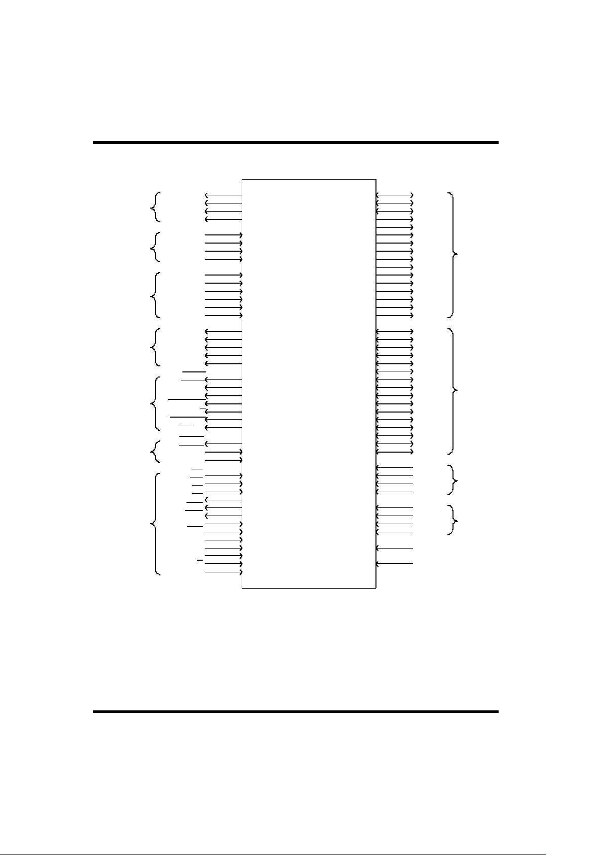
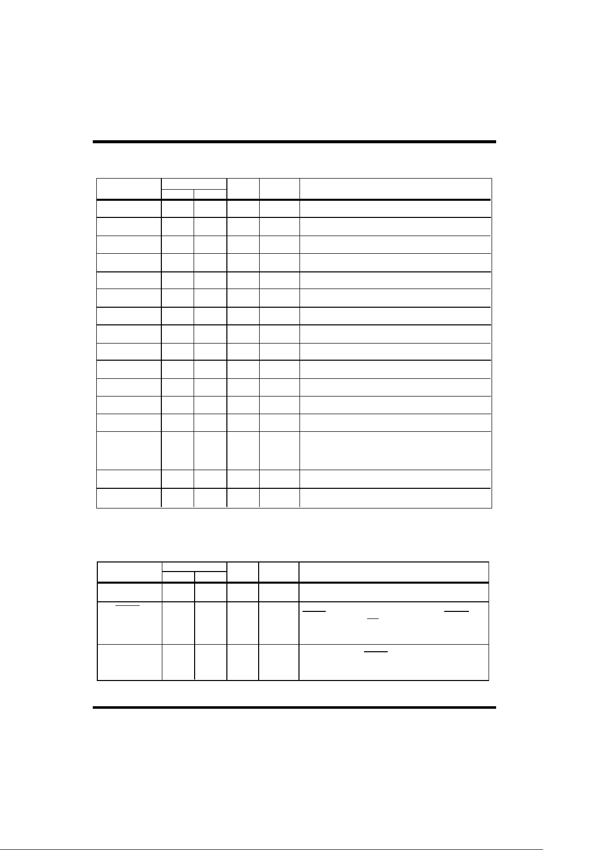
2.0 PIN IDENTIFICATION AND DESCRIPTION
Bidirectional pin.
Leadless chip carrier pinnumbers are not in parentheses.
( ) Pingrid array pin numbers are in parentheses.
(F3)
(L5)
(F10)
(A7)
(K11)
(L11)
(L2)
(K2)
(K3)
(G11)
(J6)
(G10)
(A2)
(B11)
(C11)
(C10)
(E9)
(E10)
(E11)
(E3)
(A5)
(F9)
(L7)
(C1)
(D2)
(D1)
(F2)
(E2)
(D10)
(D11)
(F11)
(B4)
(A4)
(A6)
(B5)
(C5)
(C6)
(B6)
(B7)
(C7)
(A8)
(B8)
(A9)
(A10)
(B9)
(B10)
(A11)
(L1)
(J2)
(K1)
(J1)
(H2)
(H1)
(G3)
(G2)
(G1)
(F1)
(E1)
(J5)
(H11)
(K8)
(L9)
(G9)
(H10)
(J11)
(K5)
(K6)
(L4)
(K4)
(L3)
(B3)
(A3)
(A1)
(B2)
(C2)
(B1)
(J7)
(K9)
(L10)
(K7)
(L6)
(J10)
(K10)
(L8) A
A
A
A
A
A
A
A
A
A
A
A
A
A
A
A
0
1
2
3
4
5
6
7
8
9
10
11
12
13
14
15
D
D
D
D
D
D
D
D
D
D
D
D
D
D
D
D
0
1
2
3
4
5
6
7
8
9
10
11
12
13
14
15
ADDRESS
LINES
DATA
LINES
TAZ
TAO
TBZ
TBO
RAZ
RAO
RBZ
RBO
RTA0
RTA1
RTA2
RTA3
RTA4
RTPTY
MCSA0
MCSA1
MCSA2
MCSA3
MCSA4
BIPHASE
OUT
BIPHASE
IN
MODE CODE/
SUBADDRESS
STATUS
SIGNALS
TERMINAL
ADDRESS
DMA
SIGNALS
CONTROL
SIGNALS
POWER
GROUND
CLOCK
RESET
CLK
14
12
13
41
22
40
72
51
50
52
44
46
45
49
48
47
21
38
28
29
39
37
36
19
18
17
16
15
71
73
74
75
76
77
33
34
23
25
30
31
26
27 70
69
68
67
65
64
63
61
60
59
58
57
56
55
54
53
11
10
9
8
7
6
5
4
3
2
83
82
81
80
79
78
24
43
66
84
1
20
42
62
35
32
++
++
++
++
***Pin internally pulled up.
Pin internally pulled down.
EORT
EOMC
MERR
TIMERON
CHA/B
COMSTR
MC /SA
DMAR
*DMAG
*DMAEN
RD
WR
*CS
AV
RRD
RWR
**TAPEN
*SVC
**ILLCOM
**SME
**ENBC
PRA/B
**TEST
V
SS
V
DD
V
DD
V
DD
V
DD
V
SS
V
SS
V
SS
RESET
Figure 4. RTMP Functional Pin Description
RTMP-6
Legend for TYPE and ACTIVE fields:
TO = TTL output
I = TTL input
TUI = TTL input (pull-up)
TDI = TTL input (pull-down)
TTO = Three-state TTL output
TTB = Three-state TTL bidirectioal
AH =Active high
AL = Active low
D15 78 C1 TTB Bit 15 (MSB) of the bidirectional Data bus.
DATA BUS
NAME
PIN NUMBER
LCC PGA
TYPE ACTIVE DESCRIPTION
D14
D13
D12
D10
D9
D8
D7
D6
D5
D4
D3
D2
D1
D0
79
80
81
82
83
2
3
4
5
6
7
8
9
10
11
D2
D1
F2
E2
E1
F1
G1
G2
G3
H1
H2
J1
K1
J2
L1
TTB
TTB
TTB
TTB
TTB
TTB
TTB
TTB
TTB
TTB
TTB
TTB
TTB
TTB
TTB
Bit 14 of the bidirectional Data bus.
Bit 13 of the bidirectional Data bus.
Bit 12 of the bidirectional Data bus.
Bit 11 of the bidirectional Data bus.
Bit 10 of the bidirectionalData bus.
Bit 9 of the bidirectional Data bus.
Bit 8 of the bidirectional Data bus.
Bit 7 of the bidirectional Data bus.
Bit 6 of the bidirectional Data bus.
Bit 5 of the bidirectional Data bus.
Bit 4 of the bidirectional Data bus.
Bit 3 of the bidirectional Data bus.
Bit 2 of the bidirectional Data bus.
Bit 1 of the bidirectional Data bus.
Bit 0 (LSB) of the bidirectional Data bus.
D11
--
--
--
--
--
--
--
--
--
--
--
--
--
--
--
--
RTMP-7
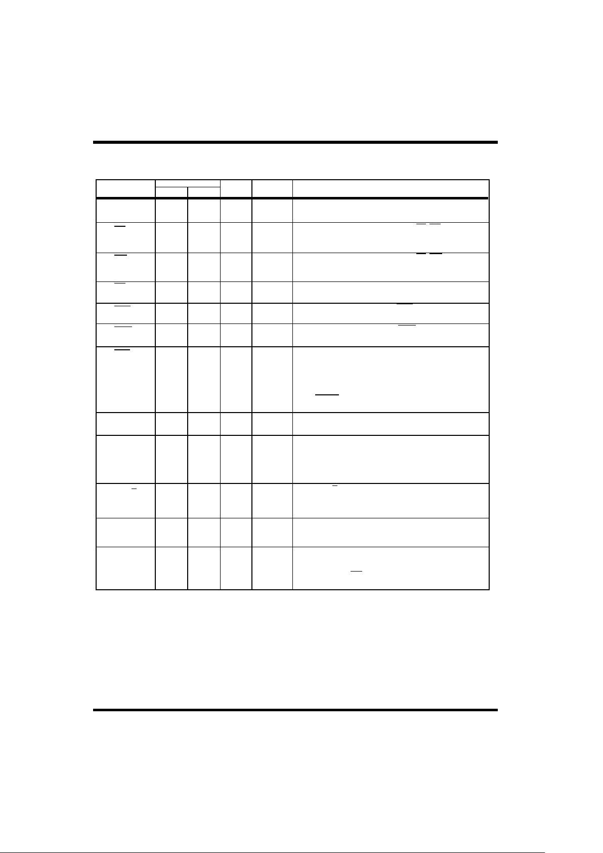
A15 53 A11 TTO Bit 15 (MSB) of the Address bus.
ADDRESS BUS
NAME
PIN NUMBER
LCC PGA
TYPE ACTIVE DESCRIPTION
A14
A13
A12
A10
A9
A8
A7
A6
A5
A4
A3
A2
A1
A0
TTO
TTO
TTO
TTO
TTO
TTO
TTO
TTO
TTO
TTO
TTO
TTO
TTB
TTB
TTB
Bit 14 of the Address bus.
Bit 13 of the Address bus.
Bit 12 of the Address bus.
Bit 11 of the Address bus.
Bit 10 of the Address bus.
Bit 9 of the Address bus.
Bit 8 of the Address bus.
Bit 7 of the Address bus.
Bit 6 of the Address bus.
Bit 5 of the Address bus.
Bit 4 of the Address bus.
Bit 3 of the Address bus.
Bit 1 of the Address Bus. (Reference A2)
Bit 0 (LSB) of the Address Bus. (Reference A2)
A11
54
55
56
57
58
59
60
61
63
64
65
67
68
69
70
B10
B9
A10
A9
B8
A8
C7
B7
B6
C6
C5
B5
A6
A4
B4
--
--
--
--
--
--
--
--
--
--
--
--
--
--
--
--
Bit 2 of the Address bus. Address bits A2 - A0 are
bidirectional so the host can select one of the RTMP’s internal
registers during internal I/O operations.
47 F11 TO
NAME
PIN NUMBER
LCC PGA
TYPE ACTIVE DESCRIPTION
DMA SIGNALS
AL DMA Request. Indicates the RTMP is requesting
DMAEN
48
49
D11
D10
TUI
TUI
AL
AH
use of the Data bus from the current bus master.
DMA Enable. When high, this input allows the
RTMP to recognize DMAG. When low, DMAEN places all
three-state pins in a high-impedance state and disables the
RTMP’s memory access cycle.
DMA Grant. Gives control of the Data bus to the RTMP.
DMAG is recognized only if DMAEN is high. DMAG must
remain asserted until AV goes high to ensure that the RTMP
completes the current DMA cycle.
DMAG
DMAR
RTMP-8
SME
ILLCOM
44 E9 TUI
NAME
PIN NUMBER
LCC PGA
TYPE ACTIVE DESCRIPTION
AL
45
46
52
50
51
40
E11
E10
C10
C11
B11
G10
TI
TI
TTO
TTO
TTO
TUI
AL
AL
AL
AL
AL
AL
Set Message Error. Asserting this input causes the
Message Error bit in thestatus word to be set.
Illegal Command. This input illegalizes a command
word that the RTMP accepts but the system does not
support. When set, the RTMP responds with the
Message Error bit set in the status word. ILLCOM
4122G11
J6
TDI
TDIAHAH
CONTROL SIGNALS
12 K2 TI
--
13
14
K3L2TDI
TDIAHAH
ENBC
TEST
Enable Broadcast. A high on this input, when the
RTMP is in the 1553B mode, allows the RTMP to
recognize a broadcast command word.
is used in conjunction with the Mode Code/
Subaddress outputs.
CS
RD
WR
AV
RRD
RWR
SVC
PRA/B
Chip Select. This input, along with RD and WR, allows
the host to access the RTMP’s internal data registers.
Read. When used in conjunction with CS, RD allows the
RTMP to place data from the selected internal register on the
Data bus (D15-D0).
Write. When used in conjunction with CS, WR latches data
from the Data bus (D15-D0) into the selected RTMP internal
register.
Address Valid. The RTMP asserts AV to indicate that the
address (A15-A0) is valid.
RAM Read. The RTMP asserts RRD during DMA cycles
that require data from system RAM.
RAM Write. The RTMP asserts RWR during DMA cycles
to write data to system memory.
Superseding Valid Command. The host system uses this
input when more than one RT is present in the system; i.e.,
a quad-redundant system. When asserted, this input causes
the RTMP to terminate all present activity and perform an
internal reset of encoders/decoders, RT state machine, and
DMA state machine. Registers are not affected. Do not assert
while DMAR is asserted (tpw 250ns minimum).
Program A/ B. This input is the 1553 mode select input. A high
input places the RTMP in the MIL-STD-1553A mode; a low
places the RTMP in the MIL-STD-1553B mode.
Test. The TEST input pin allows the user to select between
internal (TEST = 0) or external (TEST = 1) self-test. When
TEST equals a logic one and DMAEN equals a logic zero,
MCSA (4:0) and MC/SA three-state.
RTMP-9
36 J11 TTO
NAME
PIN NUMBER
LCC PGA
TYPE ACTIVE DESCRIPTION
AL
STATUS SIGNALS
MERR
37
38
39
28
29
H10
H11
G9
K8
L9
TTO
TO
TO
TO
TO
AL
AL
AH
--
AL
21 J5 TTO
NAME
PIN NUMBER
LCC PGA
TYPE ACTIVE DESCRIPTION
AL
MCSA0
MCSA1
MCSA2
MCSA3
MCSA4
15
16
17
18
19
L3
K4
L4
K6
K5
TTO
MODE CODE/SUBADDRESS
Timer On. Indicates the RTMP is transmitting data.
The output remains active until the data transmission is
complete or the internal fail-safe timer times out (600ms
for 1553A and 800ms for 1553B). The RTMP internally
disables both transmitters and keeps them disabled until the
RTMP receives a valid command word. This signal is asserted approximately 250ns
before beginning of status word transmission.
--
End of Receive/Transmit. This interrupt is a pulse that is
maskable by writing to the Control Register. The user can
select EORT to occur at the end of receive command activity,
at the end of transmit command activity, under either of these
conditions, or disable it completely. The EORT output is designed to simulate an open-collector output and requires a
pull-up resistor. (250ns pulse width). This signal is not generated if a message error condition exists.
EORT
End of Mode Code. this non-maskable interrupt is a pulse that
occurs at the end of all memory accesses associated with any
mode code command. The EOMC output is designed to simulate an open-collector output and requires a pull-up resistor.
EOMC and EORT can be logically ORed together to form a
composite interrupt. The 250ns pulse width is generated after
command word is stored. This signal is not generated if a
message error condition exists.
EOMC
COMSTR
CHA/ B
TIMERON
Message Error. Active when the RTMP detects an error in
the 1553 transmission and sets the Message Error bit in the
status word. MERR is reset when the RTMP receives the next
valid command word. (COMSTR assertion)
Channel A/ B. When high, this output indicates the RTMP
received the last command on Channel A; when low, the last
command was received on Channel B.
Mode Code/Subaddress. MC/SA = 0 indicates that the MCSAO-MCSA4 pins contain the Mode Code bits of the most
recently received mode code. MC /SA = 1 indicates that
MCSA0-MCSA4 pins contain the Subaddress bits of the
most recently received command word.
MC /SA
Mode Code/Subaddress. These five bits are used in conjunction with the MC/SA output. MC/SA = 0 indicates that these
five bits are the five least significant bits of the mode code
command word. MC /SA = 1 indicates these five bits are the
1553 command word subaddress.
Command Strobe. This low-going pulse identifies receipt of a valid 1553 command word.
RTMP-10
RTA4 73 B3 TI
NAME
PIN NUMBER
LCC PGA
TYPE ACTIVE DESCRIPTION
Remote Terminal Address Inputs. The RTMP uses
REMOTE TERMINAL ADDRESS
these inputs to select the terminal address for this
specific remote terminal.
Terminal Address Parity Enable. Enables the
RTMP’s Terminal Address parity-checking
Remote Terminal Parity. When the Terminal
Address parity-checking function is enabled
(TAPEN = 1), RTPTY must provide odd parity
for the terminal address input pins (RTA4-RTA0).
RTA3
RTA2
RTA1
RTA0
TAPEN
RTPTY
74
75
76
77
72
71
A1
B2
C2
B1
A2
A3
TDI
TI
AH
32 L11 TI
NAME
PIN NUMBER
LCC PGA
TYPE ACTIVE DESCRIPTION
MASTER RESET AND CLOCK
RAO 23 L6 TI
NAME
PIN NUMBER
LCC PGA
TYPE ACTIVE DESCRIPTION
Receiver (Channel) A One. Manchester input from
CHANNEL A BIPHASE SIGNALS
AL
CLK 35 K11 TI
the 1553 bus receiver.
Receiver (Channel) A Zero. This input is the
complement of RAO.
Transmitter (Channel) A One. This Manchester-
encoded data output is connected to the 1553 bus
transmitter input. The output is idle low.
Transmitter (Channel) A Zero. This output is
the complement of TAO. The output is idle low.
RAZ
TAO
TAZ
25
26
27
K7
J7
L8
TI
TO
TO
function.
--
--
--
--
--
--
--
RESET
Reset. Initializes all internal functions of the RTMP.
RESET must be asserted before normal RTMP operation.
Clock. The clock input requires a 50% ± 10% duty cycle
with an accuracy of 12MHz ± 0.01%.
RTMP-11
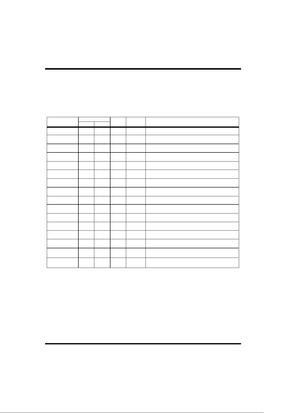
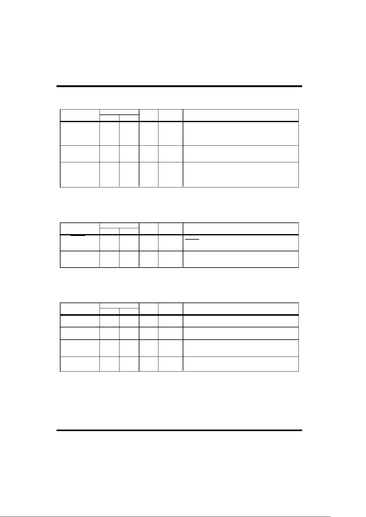
3.0 REMOTE TERMINAL ARCHITECTURE
3.1 Internal Registers
The RTMP has six internal registers that allow the host to
control the RTMP’s actions and also to obtain its operational
status. The host can read from or write to three of these
registers: the Time Tag Data Register (TTD), the Control
Register (CTL), and the Base Pointer Data Register (BPD).
Two of the registers are read-only: the Operational Status
Register (OPS), and the Last Command Register (LCM).
The Stop Self-Test Register (SST) is a write-only register.
Six signals allow the host to access the RTMP’s internal
registers. Three of the six signals are control signals: Chip
Select (CS), Read (RD ), and Write (WR). The other three
signals are the RTMP’s bidirectional address lines, A0 - A2.
When the CS = 0, the three least significant address lines,
A0 - A2, become inputs to the RTMP. The RTMP decodes
these three address lines, along with CS, RD , and WR, to
determine which of the six internal registers the host is
attempting to access. Table 1 shows the addresses for the
RTMP’s internal registers for read and write operations.
3.2 Read/Write Registers
The RTMP has three internal read/write registers. These
three registers are:
• The Time Tag Data Register
• The Control Register
• The Base Pointer Data Register
Time Tag Data Register (TTD)
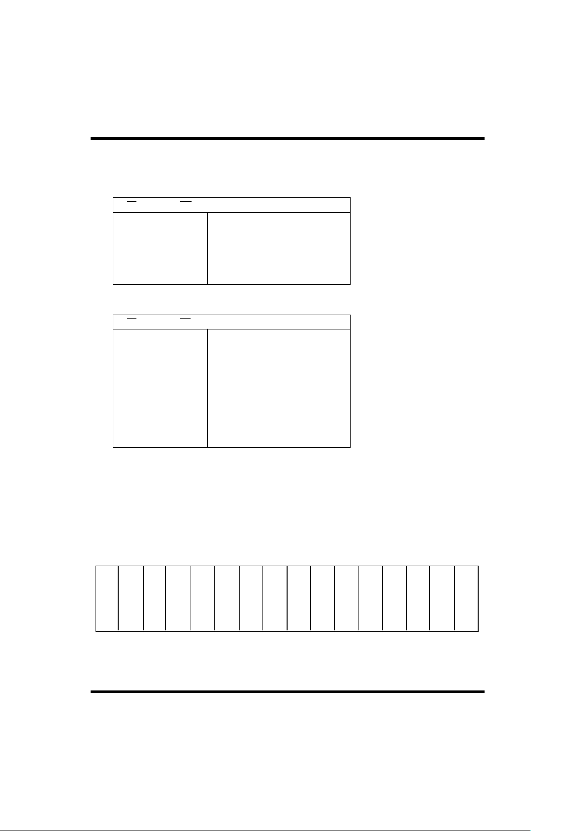
The TTD contains a free-running, 16-bit, ripple counter.
The Time Tag clock has a resolution of 64ms. The TTD is
initialized to 0000H when the host asserts the RESET input.
All TTD bits are programmable by performing a write to
the TTD with the desired bit pattern.
The RTMP stores the TTD’s value in the shared memory
area at the end of each 1553 receive message. The host can
also directly read the TTD. Since the TTD is a free-running
counter, the host may read the TTD while the counter is
rippling, resulting in the host reading erroneous data. If this
situation presents a problem, the host should read the TTD
data twice. Figure 5 represents the TTD. (0000H after
Master Reset.)
RBO 33 K10 TI
NAME
PIN NUMBER
LCC PGA
TYPE ACTIVE DESCRIPTION
Receiver (Channel) B One. Manchester data input
CHANNEL B BIPHASE SIGNALS
from the 1553 bus receiver.
Receiver (Channel) B Zero. This input is the
complement of RBO.
Transmitter (Channel) B One. This Manchester-
encoded output is connected to the 1553 bus
transmitter input. The output is idle low.
Transmitter (Channel) B Zero. This output is the
complement of TBO. The output isidle low.
RBZ
TBO
TBZ
34
30
31
J10
L10
K9
TI
TO
TO
24 L7
NAME
PIN NUMBER
LCC PGA
TYPE ACTIVE DESCRIPTION
POWER AND GROUND
43
66
84
1
20
42
62
F9
A5
E3
F3
L5
F10
A7
--
--
--
--
--
--
--
--
+5 VDC Power. Power supply input must be
Reference Ground. Zero VDC logic ground.
V
DD
V
SS
RTMP-12
Table 1. RTMP Internal Register Addresses
1. RTMP Register Write Addresses
A2 A1 A0
0
0
0
0
0
0
0
0
0
0
0
0
0
0
1
1
0
1
0
1
Time Tag Data Register
Control Register
Base Pointer Data Register
Stop Self-Test Register
2. RTMP Register Read Addresses
A2 A1 A0
0
0
0
0
0
0
0
0
0
0
0
0
0
0
1
0
0
1
1
0
0
1
0
1
0
Time Tag Data Register
Control Register
Base Pointer Data Register
Operational Status Register
Last 1553 Command Register
0 0 1 X X Don’t Care
0
0
0
0
0
0
1
1
1
0
1
1
1
0
1
Don’t Care
Don’t Care
Don’t Care
CS WR
CS RD
15 14 13 12 11 10 9 8 7 6 5 4 3 2 1 0
C
N
T
1
5
C
N
T
1
4
C
N
T
1
3
C
N
T
1
2
C
N
T
1
1
C
N
T
1
0
C
N
T
9
C
N
T
8
C
N
T
7
C
N
T
6
C
N
T
5
C
N
T
4
C
N
T
3
C
N
T
2
C
N
T
1
C
N
T
0
MSB LSB
Figure 5. The Time Tag Data Register
 Loading...