

Aeroflex UTMC UT06MRA500, UT06MRA450, UT06MRA600, UT06MRA550, UT06MRA400 Datasheet
...
Semicustom Products
UT0.6µCRΗ/SRH Commercial RadHardTM and Strategic
RadHard
TM
Gate Array Family
Data Sheet May 2002
FEATURES
q Multiple gate array sizes up to 600,000 usable equivalent
gates
q Toggle rates up to 150 MHz
q Advanced 0.6µ (0.5µL
eff
) radiation-tolerant silicon gate
CMOS processed in a commercial fab
q Operating voltage of 5V and/or 3.3V
q QML Class Q & V compliant
q Designed specifically for high reliability applications
q Commercial RadHardTM for radiation-tolerant to 300K
rads to meet space requirements and SEU-immune to less
than 2.0E-10 errors/bit-day
q Strategic RadHardTM for radiation environments to 1
Mega rads to meet space requirements and SEU-immune
to less than 2.0E-10 errors/bit-day
q JTAG (IEEE 1149.1) boundary-scan supported
q Low noise package technology for high speed circuits
q Design support using Mentor Graphics® and SynopsysTM
in VHDL or Verilog design languages on Sun® and Linux
workstations
q Supports cold sparing fo r power down applications
q Supports voltage translation
- 5V bus to 3.3V bus
- 3.3V bus to 5V bus
PRODUCT DESCRIPTION
The high-performance UT0.6 µCRH/SRH gate array family
features densities up to 600,000 equivalent gates and is available in MIL-PRF-38535 QML Q and V product assurance
levels and is radiation-tolerant.
The Commercial RadHardTM and Strategic RadHardTMsilicon is fabricated at American Microsystems Incorporated
(AMI) using a minimally invasive processing module, developed by UTMC, that enhances the total dose radiation
hardness of the field and gate oxides while maintaining circuit
density and reliability. In addition, for both greater transient
radiation-hardness and latchup immunity, the UTMC 0.6µ
process is built on epitaxial substrate wafers.
Developed using UTMC’s patented architectures, the
UT0.6µCRH/SRH gate array family uses a highly efficient
continuous column transistor architecture for the internal cell
construction. Combined with state-of-the-art placement and
routing tools, the utilization of available transistors is maximized using three levels of metal interconnect.
The UT0.6 µCRH/SRH family of gate arrays is supported by
an extensive cell library that includes SSI, MSI, and 54XX
equivalent functions, as well as configurable RAM and cores.
UTMC’s core library includes the following functions:
• Intel 80C31® equivalent
• Intel 80C196® equivalent
• MIL-STD-1553 functions (BRCTM, RTI, RTMP)
• MIL-STD-1750 microprocessor
• RISC microcontroller
• Configurable RAM (SRAM, DPSRAM)
• USART (8 2C51)
• EDAC
2
Table 1. Gate Densities
Notes:
1.Based on NAND2 equivalents. Actual usable gate count is design-dependent. Estimates reflect a mix of functions including RAM.
2.Includes five pins that may or may not be reserved for JTAG boundary-scan, depending on user requirements.
3.Reserved for dedicated VDD/VSS and V
DDQ/VSSQ
.
Low-noise Device and Package Solutions
The UT0.6µCRH/SRH array family’s output drivers feature pro-
grammable slew rate control for minimizing noise and switching
transients. This feature allows the user to optimize edge characteristics to match system requirements. Separate on-chip power
and ground buses are provided for internal cells and output drivers which further isolate internal design circuitry from switching
noise.
In addition, Aeroflex UTMC offers advanced low-noise package
technology with multi-layer, co-fired ceramic construction featuring built-in isolated power and ground planes (see Table 2).
These planes provide lower overall resistance/inductance
through power and ground paths which minimize voltage drops
during periods of heavy switching. These isolated planes also
help sustain supply voltage during dose rate events, thus preventing rail span collapse.
Flatpacks are available with up to 352 leads; PGAs are available
with up to 299 pins and LGAs to 472 pins. Aeroflex UTMC’s
flatpacks feature a non-conductive tie bar that helps maintain
lead integrity through test and handling operations. In addition
to the packages listed in Table 2, Aeroflex UTMC offers custom
package development and package tooling modification services
for individual requirements.
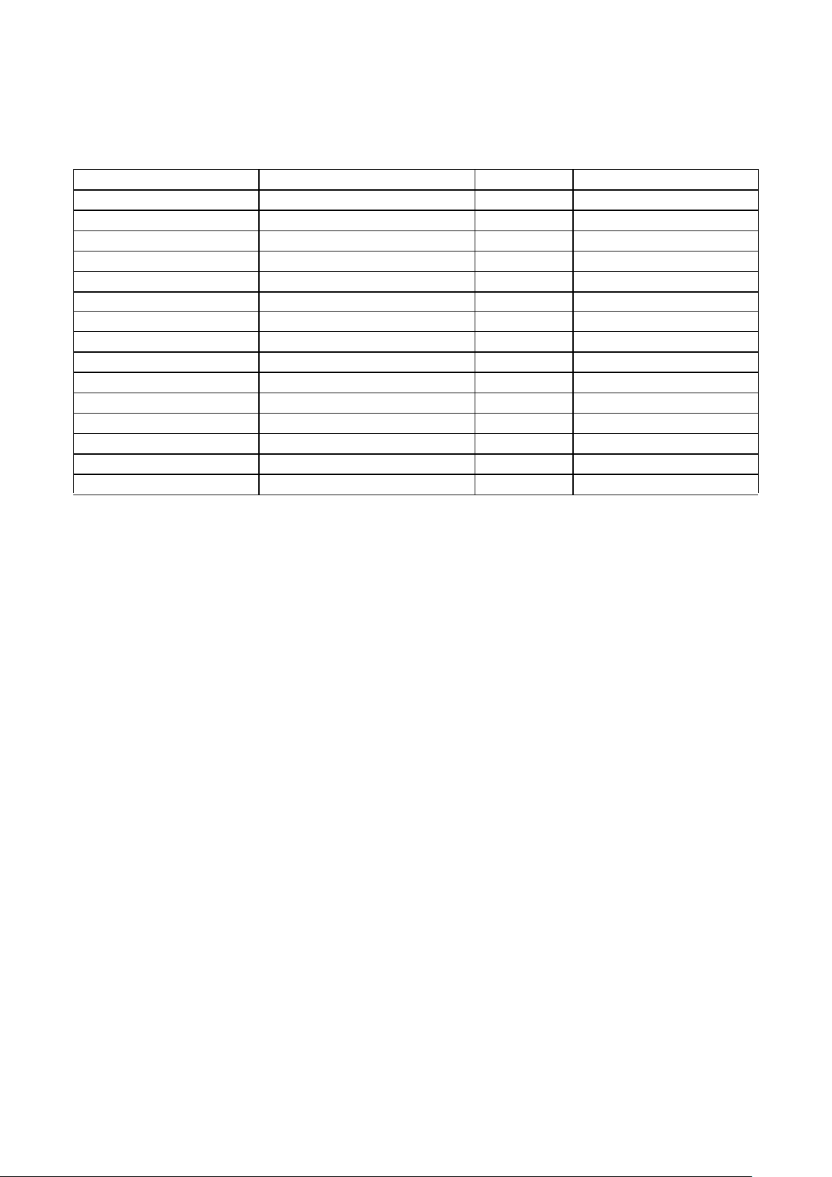
DEVICE PART NUMBERS EQUIVALENT USABLE GATES1SIGNAL I/O2POWER & GROUND PADS
3
UT06MRA010 10,000 58 6
UT06MRA025 25,000 192 48
UT06MRA050 50,000 192 48
UT06MRA075 75,000 308 76
UT06MRA100 100,000 308 76
UT06MRA150 150,000 308 76
UT06MRA200 200,000 432 96
UT06MRA250 250,000 432 96
UT06MRA300 300,000 432 96
UT06MRA350 350,000 432 96
UT06MRA400 400,000 544 144
UT06MRA450 450,000 544 144
UT06MRA500 500,000 544 144
UT06MRA550 550,000 544 144
UT06MRA600 600,000 544 144
3
Table 2. Packages
Notes:
1. The number of device I/O pads available may be restricted by the selected package.
2. PGA packages have one additional non-connected index pin (i.e., 84 + 1 index pin = 85 total package pins for the 85 PGA).
Contact Aeroflex UTMC for specific package drawings.
PACKAGE
TYPE/
LEADCOUNT
1
025 050 075 100 150 200 250 300 350 400 450 500 550 600
Flatpack
68 X X X
84 X X
132 X X
172 X X X X X
196 X X X X X
256 X X X X X X X X X
304 X X X X X X X X X
340 X X X X X X X X X
352 X X X X X
PGA
2
281 X X X X
299 X X X X
LGA
472 X X X X
4
Extensive Cell Library
The UT0.6µCRH/SRH family of gate arrays is supported by an
extensive cell library that includes SSI, MSI, and 54XX-equivalent functions, as well as RAM and other library functions. Userselectable options for cell configurations include scan for all register elements, as well as output drive strength. Aeroflex
UTMC’s core library includes the following functions:
• Intel® 80C31 equivalent
• Intel® 80C196 equivalent
• MIL-STD-1553 functions (BCRTM, RTI, RTMP)
• MIL-STD-1750 microprocessor
• Standard microprocessor peripheral functions
• Configurable RAM (SRAM, DPsRAM)
• RISC Microcontroller
• USART (82C51)
• EDAC
Refer to Aeroflex UTMC’s UT0.6µCRH/SRH Design Manual
for complete cell listing and details.
I/O Buffers
The UT0.6 µCRH/SRH gate array family offers up to 544 signal
I/O locations (note: device signal I/O availability is affected by
package selection and pinout.) The I/O cells can be configured
by the user to serve as input, output, bidirectional, three-state, or
additional power and ground pads. Output drive options range
from 2 to 12mA. To drive larger off-chip loads, output drivers
may be combined in parallel to provide additional drive up to
24mA.
Other I/O buffer features and options include:
• Slew rate control
• Pull-up and pull-down resistors
• TTL, CMOS, and Schmitt levels
• Cold sparing
• Voltage translation
- 5V bus to 3.3V bus
- 3.3V bus to 5V bus
JTAG Boundary-Scan
The UT0.6 µCRH/SRH arrays provide for a test access port and
boundary-scan that conforms to the IEEE Standard 1149.1
(JTAG). Some of the benefits of this capability are:
• Easy test of complex assembled printed circuit
boards
• Gain access to and control of internal scan paths
• Initiation of Built-In Self Test
Clock Driver Distribution
Aeroflex UTMC design tools provide methods for balanced
clock distribution that maximize drive capability and minimize
relative clock skew between clocked devices.
Speed and Performance
Aeroflex UTMC specializes in high-performance circuits designed to operate in harsh military and radiation environments.
Table 3 presents a sampling of typical cell delays.
Note that the propagation delay for a CMOS device is a function
of its fanout loading, input slew, supply voltage, operating temperature, and processing radiation tolerance. In a radiation
environment, additional performance variances must be considered. The UT0.6µCRH/SRH array family simulation models
account for all of these effects to accurately determine circuit
performance for its particular set of use conditions.
Power Dissipation
Each internal gate or I/O driver has an average power consumption based on its switching frequency and capacitive loading.
Radiation-tolerant processes exhibit power dissipation that is
typical of CMOS processes. For a rigorous power estimating
methodology, refer to the Aeroflex UTMC UT0.6µCRH/SRH
Design Manual or consult with a Aeroflex UTMC Applications
Engineer.
Typical Power Dissipation
1.1µW/Gate-MHz@5.0V 0.4µW/Gate-MHz@3.3V
5
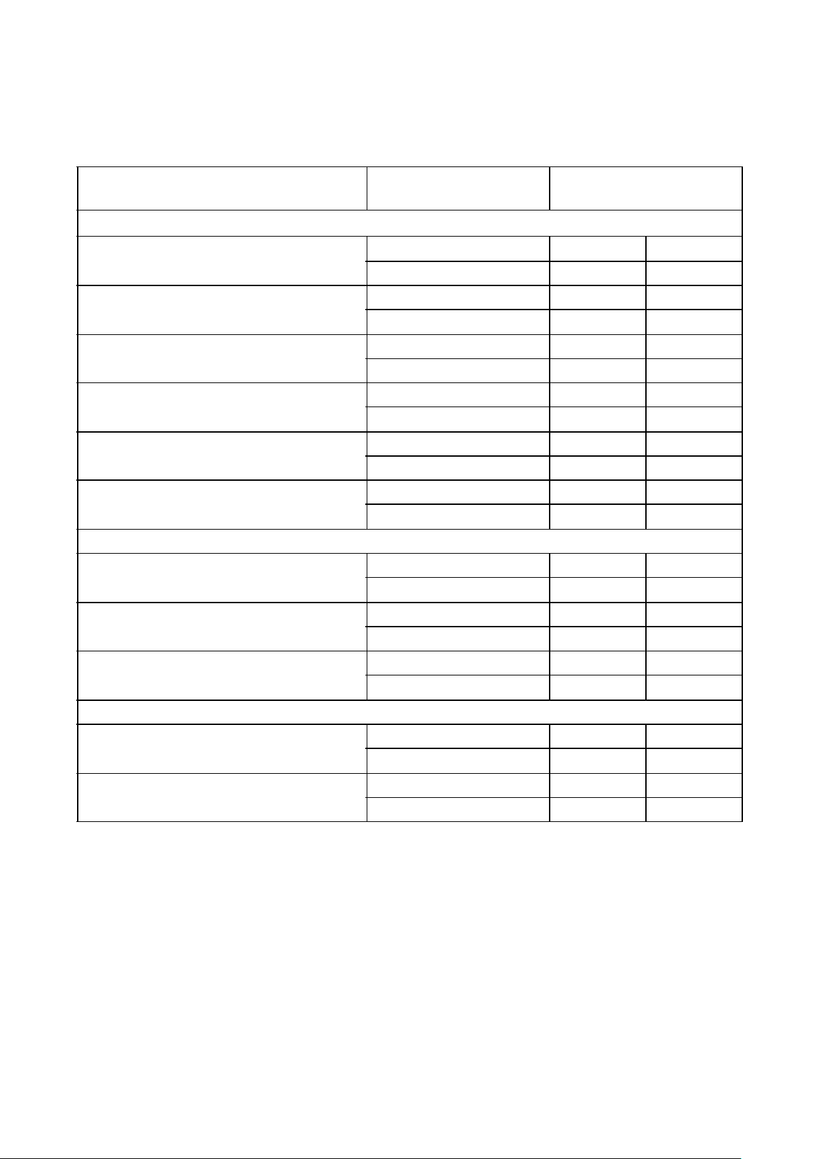
Table 3. Typical Cell Delays
Note:
1. All specifications in ns (typical). Output load capacitance is 50pF. Fanout loading for input buffers and gates is the equivalent of two gate input loads.
CELL OUTPUT
TRANSITION
PROPAGATION
DELAY
1
Internal Gates V
DD
= 5.0V V
DD
= 3.3V
INV1, Inverter HL .15 .16
LH .23 .29
INV4, Inverter 4X HL .06 .07
LH .10 .16
NAND2, 2-Input NAND HL .19 .25
LH .22 .33
NOR2, 2-Input NOR HL .16 .22
LH .32 .45
DFF - CLK to Q HL .81 1.12
LH .76 1.06
HL .75 1.05
LH .61 .85
Output Buffers
OC5050N4, CMOS HL 3.85 2.15
LH 4.66 3.76
OT5050N4, TTL, 4mA HL 5.58 5.49
LH 2.52 2.93
OT5050N12, TTL, 12mA HL 2.42
LH 1.29
Input Buffers
IC5050, CMOS HL .81 1.07
LH 1.16 1.18
IT5050, TTL HL 1.39 1.12
LH 1.16 1.30
 Loading...