

Page 1

RAMP Wireless Module
RM024
Hardware Integration Guide
Version 3.1
Americas: +1-800-492-2320 Option 2
Europe: +44-1628-858-940
Hong Kong: +852-2923-0610
www.lairdtech.com/ramp
Page 2

RM024 Hardware Integration Guide
Americas: +1-800-492-2320 Option 2
Europe: +44-1628-858-940
Hong Kong: +852-2923-0610
www.lairdtech.com/wireless
2
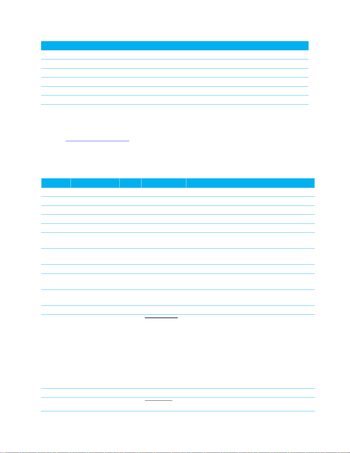
CONN-HIG_RAMP24
Rev.
Revision Date
Description
1.0
Initial Version
2.1
Added firmware changes, updated the name of the Force 9600 Pin,
removed old references to LT2510 part numbers, added new
information on cyclic sleep and Antenna Switch Override. Added a
table under Max Power and a table for the Set Max Power command.
2.2
Minor grammatical fixes.
2.3
27 June 2013
PWM output data was corrected to a 39.3846 µS period vs. 315.077, as
was stated previously.
2.4
12 July 2013
Minor edits, removed Firmware History and references irrelevant to
RM024.
2.5
10 Oct 2013
Corrected Antenna Select Override information error. Changed 0x59
to 0x5B
3.0
10 Dec 2013
Separated Hardware Integration Guide (HIG) from User Guide
information (created two separate documents).
Add Related Documents section.
3.1
10 Jan 2014
Added 10 mW version information.
Version 3.1
REVISION HISTORY
Page 3

RM024 Hardware Integration Guide
Americas: +1-800-492-2320 Option 2
Europe: +44-1628-858-940
Hong Kong: +852-2923-0610
www.lairdtech.com/wireless
3
CONN-HIG_RAMP24
Version 3.1
CONTENTS
Revision History ................................................................................................................................................... 2
Contents .............................................................................................................................................................. 3
RAMP Modules ................................................................................................................................................... 4
Overview ........................................................................................................................................................ 4
Key Features .................................................................................................................................................. 4
Detailed Specifications ............................................................................................................................... 5
Pin Definitions ................................................................................................................................................. 7
Input Characteristics .................................................................................................................................... 8
Output Characteristics ................................................................................................................................ 8
Block Diagram ............................................................................................................................................... 9
Timing Specifications .................................................................................................................................... 9
RF Hop Frame .............................................................................................................................................. 10
Hardware Interface ........................................................................................................................................ 12
Pin Descriptions ........................................................................................................................................... 12
Mechanical Considerations .......................................................................................................................... 14
Mechanical Drawing ................................................................................................................................. 14
Ordering Information ...................................................................................................................................... 18
Product Part Numbers ................................................................................................................................ 18
Regulatory Information .................................................................................................................................. 19
FCC/IC Requirements for Modular Approval ........................................................................................ 19
CE Requirements for Modular Approval ................................................................................................ 21
Japan Requirements for Modular Approval ......................................................................................... 22
Related Documents ........................................................................................................................................ 24
Page 4

RM024 Hardware Integration Guide
Americas: +1-800-492-2320 Option 2
Europe: +44-1628-858-940
Hong Kong: +852-2923-0610
www.lairdtech.com/wireless
4
CONN-HIG_RAMP24
Version 3.1
RAMP MODULES
Laird RAMP (Range Amplified MultiPoint) modules are designed to provide robust wireless
communications for any number of applications requiring a wireless transport for serial data.
RAMP modules feature a Frequency Hopping Spread Spectrum (FHSS) protocol for excellent
interference and multipath immunity. RAMP modules server/client architecture allows for more
than 16 million clients to be addressed and communicating within the network.
Overview
The RM024 RAMP module is based on Laird LT2510 core technology, enhanced with a new RF
front end for improved sleep, improved link budget, and a switchable antenna output. The
RM024 is available in two versions, one with 125 mW maximum conducted output power which is
approved for North American and similar markets, and one with 10 mW maximum conducted
output power which is approved for European and similar markets. These modules are identical
except for output power, transmit power consumption, and the number of RF channels
available. Differences between the two versions, where applicable, are denoted based on part
number.
This document contains information about the hardware and software interface between a
Laird RM024 transceiver and an OEM host. Information includes the theory of operation,
specifications, interface definitions, and mechanical drawings.
Note: Unless mentioned specifically by name, the RM024 modules are referred to as “radio”
or “transceiver”. Individual naming is used to differentiate product specific features.
The host (PC/microcontroller/any device to which the RM024 module is connected)
are referred to as “OEM host” or “host.”
Key Features
Retries and acknowledgements
Configurable network parameters
Multiple generic I/O
280 kbps or 500 kbps RF data stream
Idle current draw of 9.5 mA, sleep current of 50 uA
Software selectable interface baud rates from 1200 bps to 460.8 kbps
Upgradable FW through serial port
Low cost, low power, and small size ideal for high volume, portable, and battery powered
applications
All modules are qualified for Industrial temperatures (-40°C to 85°C)
Advanced configuration available using AT commands
Easy to use Configuration and Test Utility software
Switchable antenna output, either integrated antenna or external antenna through U.FL
Page 5

RM024 Hardware Integration Guide
Americas: +1-800-492-2320 Option 2
Europe: +44-1628-858-940
Hong Kong: +852-2923-0610
www.lairdtech.com/wireless
5
CONN-HIG_RAMP24
GENERAL
Form Factor
SMD-ANT+U.FL, Pluggable-ANT+U.FL, SMD-U.FL,
Pluggable-U.FL
Antenna
External antenna through U.FL connector or dual
antenna with integrated antenna and U.FL
Serial Interface Data Rate
Baud rates from 1200 to 230400. Non-standard
baud rates are also supported.
Channels
FCC: 42 or 78 selectable channels
CE: 42 selectable channels
Security
Channelization, System ID, and Vendor ID
Minimum Flash (EEPROM) Memory
Endurance
1000 Write/Erase Cycles
TRANSCEIVER
Frequency Band
2400 – 2483.5 MHz
RF Data Rate (Raw)
280 kbps or 500 kbps selectable
Hop Bin Spacing
900 kHz over 79 hops
1500 kHz over 43 hops
RF Technology
Frequency Hopping Spread Spectrum
Modulation
MSK
Maximum Output Power Conducted1
FCC: +5 to +21 dBm selectable
CE: +3.5 to +18 dBm selectable
Supply Voltage
2.3 – 3.6 V ± 50 mV ripple
Current Draw2
RM024 Version
FCC(125mW)
CE(10mW)
100% Tx
136 mA
40 mA
1/8 Tx (when
selected)
40 mA
40 mA
100% Rx
36 mA
36 mA
Rx average (idle
9.5 mA
9.5 mA
Deep sleep
.38 µA
.38 µA
Receiver Sensitivity (1% PER)
-95 dBm at 280 kbps RF Data Rate
-94 dBm at 500 kbps RF Data Rate
Range (based on external 2.0 dBi
antenna at 280 kbps RF Data Rate)3
Outdoor (line-ofsight)
Indoor
(estimated)
FCC
2.5 miles (4 km)
1300 ft (400 m)
CE
.6 miles (1.0 km)
328 ft (100 m)
ENVIRONMENTAL
Temperature (Operational)
-40ºC to 85ºC
Temperature (Storage)
-50ºC to 150ºC
PHYSICAL
Version 3.1
Detailed Specifications
Table 1: Detailed Specifications
Page 6

RM024 Hardware Integration Guide
Americas: +1-800-492-2320 Option 2
Europe: +44-1628-858-940
Hong Kong: +852-2923-0610
www.lairdtech.com/wireless
6
CONN-HIG_RAMP24
SMD-Multi Antenna Dimensions
1.0” x 1.54” x 0.14” (25.4 mm x 39 mm x 3.6 mm)
SMD-U.FL Dimensions
1.0” x 1.28” x 0.14” (25.4 mm x 32.4 mm x 3.6 mm)
Pluggable-Multi Antenna Dimensions
1.05” x 1.56” x 0.44” (26.7 mm x 39.6 mm x 11.3 mm)
Pluggable-U.FL Dimensions
1.05” x 1.29” x 0.42” (26.7 mm x 33 mm x 10.6 mm)
Version 3.1
Page 7
RM024 Hardware Integration Guide
Americas: +1-800-492-2320 Option 2
Europe: +44-1628-858-940
Hong Kong: +852-2923-0610
www.lairdtech.com/wireless
7
CONN-HIG_RAMP24
CERTIFICATIONS
FCC Part 15.247
KQL-RM024
Industry Canada (IC)
2268C-RM024
CE
Yes, RM024-x10-x versions
RoHS
Yes
Japan (TELEC) 4
Yes, RM024-x50-x versions
Brazil (Anatel)
5
None
SMT Pin
Pluggable Pin
Type
Signal Name
Functions
1 7 O
GIO_0
Generic Output / Hop_Frame
2 6 O
GIO_1
Generic Output
3 8
DNC
Do Not Connect
4
17 O GIO_2
RS485 Driver Enable
5
19 O GIO_3
PWM Output
6 3 I
RXD
Asynchronous serial data input to
transceiver
7 2 O
TXD
Asynchronous serial data output from
transceiver
8
10
GND
GND
Signal Ground
9 1 PWR
Vcc
2.3 – 3.6 V ±50 mV ripple (must be
connected)
10 - PWR
Vpa
2.3 - 3.6 V ±5 0mV ripple (must be
connected)
11 - GND
GND
Signal Ground
12 9 I
Force 9600
/Sleep
Interrupt
Force 9600 – When pulled logic Low and
then applying power or resetting, the
transceiver’s serial interface is forced to a
9600, 8-N-1 rate.
Sleep Interrupt- When taken low this pin will
wake the radio from sleep
Note: Because this mode disables some
modes of operation, it should not be
permanently pulled Low during
normal operation.
13
14 I GIO_4
Generic Input
14 5 I
µP_Reset
RESET – Controlled by the RM024 for power-
Version 3.1
1. Maximum Output power stated, step measurements for power could vary by +/- 2.0 dBm.
2. Sleep currents are estimated
3. Range distances are estimated, measurements were taken at 4.1 miles with 5 dBi antenna
for FCC module
4. See Regulatory Information in this manual
5. Contact your sales representative for more details.
Pin Definitions
Table 2: Pin Definitions
Page 8
RM024 Hardware Integration Guide
Americas: +1-800-492-2320 Option 2
Europe: +44-1628-858-940
Hong Kong: +852-2923-0610
www.lairdtech.com/wireless
8
CONN-HIG_RAMP24
SMT Pin
Pluggable Pin
Type
Signal Name
Functions
on reset if left unconnected. After a stable
power-on reset, a logic Low pulse will reset
the transceiver.
15
11
I
CMD/Data
When logic Low, the transceiver interprets
incoming OEM host data as command
data. When logic High, the transceiver
interprets OEM host data as transmit data.
16
15
O
In Range
When logic Low, the client is in range and
synchronized with a server. This will always
be Low on a server.
17
16
I
RTS
Request to Send. Floats high if left
unconnected. When enabled in EEPROM,
the module will not transmit data out the
Serial UART unless the pin is Low.
18
12
O
CTS
Clear to Send - CTS is used for hardware
flow control. CTS will toggle high when the
input buffer reaches the CTS On threshold
until the buffer recedes below CTS Off.
19
18 GIO_8
Generic Input
1
20
13 GIO_5
Reserved for future use. Do not connect.
21 4
GIO_6
Reserved for future use. Do not connect.
22
20 I GIO_7
Analog to Digital Input
Signal Name
High Min.
High Max.
Low Min.
Low Max.
µP_Reset
0.8 v
Vcc
0 v
0.6 v
RTS
2.31 v
Vcc
0 v
.99 v
AD_In
N/A
Vcc
0 v
N/A
All other inputs
70% Vcc
Vcc
0 v
30% Vcc
Signal Name
High Min.
High Max.
Low Min.
Low Max.
Sink Current
Version 3.1
Tips:
All I/O directions are referenced to Vcc.
All inputs are weakly pulled High via a 20k Ohm pull-up resistor and may be left floating
during normal operation
Minimum connections: VCC, VPA, GND, TXD, & RXD
Signal direction is with respect to the transceiver
Unused pins should be left disconnected
Input Characteristics
Table 3: Input Characteristics
Output Characteristics
Table 4: Output Characteristics
Page 9

RM024 Hardware Integration Guide
Americas: +1-800-492-2320 Option 2
Europe: +44-1628-858-940
Hong Kong: +852-2923-0610
www.lairdtech.com/wireless
9
CONN-HIG_RAMP24
GO_0
2.5 v
3.3 v
0 v
0.4 v
20 mA
GO_1
2.5 v
3.3 v
0 v
0.4 v
20 mA
PWM_Output
N/A
3.3 v
0 v
N/A
4 mA
All other
inputs
2.5 v
3.3 v
0 v
0.4 v
4 mA
Parameter
Server/Client
Min.
Typ.
Max.
Notes
Power on to
CTS Low
5 ms
10 ms
N/A
The first boot after a FW
upgrade will require more
than the typical amount of
time for CTS to toggle Low.
EEPROM
Read
800 µs
1 ms
2 ms
Measured from last byte of
command to first byte of
response: 870 µs for 1 byte
1.1 ms for 80 bytes 1.4 ms
for 256 bytes
EEPROM Write
20 ms
30 ms
40 ms
Measured. EEPROM writes
will cause the radio to
resynchronize
Power on to
In Range
Client only,
server will go
in range in
13 ms
600 ms
1700 ms
1
Maximum time assuming all
beacons are heard, RF
interference could extend
Version 3.1
Block Diagram
Figure 1: Block Diagram of RM024
Timing Specifications
Table 5: Timing Specifications
Page 10

RM024 Hardware Integration Guide
Americas: +1-800-492-2320 Option 2
Europe: +44-1628-858-940
Hong Kong: +852-2923-0610
www.lairdtech.com/wireless
10
CONN-HIG_RAMP24
Parameter
Server/Client
Min.
Typ.
Max.
Notes
fewer than 13
ms
the maximum time
indefinitely
Hope Period
In Range
13.19 ms
Hop Period
Out of Range
Client only
38.4 ms
Reset Pulse
250 ms
PWM Output
Period
39.3846 µs
Restore
Default
EEPROM
Command
10 ms
38 ms
Restore command also
initiates a soft reset, so
monitoring CTS is the best
indication of a completed
command
Non Specific
AT Command
1 ms
10 ms
Some AT Commands could
wait indefinitely for a
response
Write Flash
For FW Upgrade
Read Flash
Decrypt
Image
Version 3.1
RF Hop Frame
The RM024 hops every 13.19 ms and can be configured for two different RF data rates to provide
options for range or throughput. During each hop, the RM024 reserves a certain amount of time
for overhead such as the synchronization beacon, internal messaging, and user data
transmission. The diagrams below outline the various transmissions that occur during a hop. These
transmissions are transparent to the user sending data, but may be useful for applications that
require critical timing. User data is only transmitted during the data slots and after the Interface
Timeout or RF Packet Size criteria has been met. Data transmission only begins at the beginning
of a data slot. When configured for Full Duplex, data slot 1 is reserved for the server and data slot
2 is shared by all clients for transmissions.
Page 11

RM024 Hardware Integration Guide
Americas: +1-800-492-2320 Option 2
Europe: +44-1628-858-940
Hong Kong: +852-2923-0610
www.lairdtech.com/wireless
11
CONN-HIG_RAMP24
Version 3.1
Figure 2: RF Hop Frame
Page 12

RM024 Hardware Integration Guide
Americas: +1-800-492-2320 Option 2
Europe: +44-1628-858-940
Hong Kong: +852-2923-0610
www.lairdtech.com/wireless
12
CONN-HIG_RAMP24
Version 3.1
HARDWARE INTERFACE
Pin Descriptions
RXD and TXD
The RM024 accepts 3.3 VDC TTL level asynchronous serial data from the OEM host via the RXD
pin. Data is sent from the transceiver, at 3.3 V levels, to the OEM host via the TXD pin. Pins should
be left floating or high when not in use. Leaving the RXD tied low results in the radio transmitting
garbage serial data across the RF.
Force 9600 /Sleep Interrupt
When pulled logic Low before applying power or resetting, the transceiver’s serial interface is
forced to 9600, 8-N-1 (8 data bits, No parity, 1 stop bit): regardless of the actual EEPROM setting.
RTS is ignored, the interface timeout is also set to 3 ms and the RF packet size is set to the default
size for the selected RF data rate. To exit, the transceiver must be reset or power-cycled with the
test pin logic High or disconnected. When in Force 9600 mode, the radio’s receiver is disabled.
When enabled in the EEPROM, 9600 Boot option causes the 9600 pin to be ignored on cold boot
(power-up), command boot (0xCC 0xFF), and brown-out conditions. Therefore, the 9600 pin is
only observed on warm boots (reset pin toggled). This can be helpful so that brown-out
conditions don’t cause the baud rate to change if the 9600 pin happens to be low at the time.
When 9600 Boot option is disabled, the 9600 pin is used for all boot conditions. 9600 Boot option is
enabled by default.
Force 9600 is also used to wake the radio from sleep. When the pin is taken low, the radio wakes.
The transceiver does not sleep if the pin is low when the sleep command is issued.
Note: Because this pin disables some modes of operation, it should not be permanently
pulled low during normal operation.
µP_RESET
µP_Reset provides a direct connection to the reset pin on the RM024 microprocessor and is
used to force a hard reset. For a valid reset, reset must be asserted Low for an absolute minimum
of 250 ns.
Command/Data
When logic High, the transceiver interprets incoming serial data as transmit data to be sent to
other transceivers. When logic Low, the transceiver interprets incoming serial data as command
data. When logic Low, data packets from the radio are not transmitted over the RF interface,
however, incoming packets from other radios are still received. Enabling CMD/Data RX Disable
in the EEPROM causes incoming RF packets to be queued by the receiving radio while
CMD/Data is low. When CMD/Data goes high, the data is sent over the serial interface.
In_Range
The In_Range pin is driven low when a client radio’s frequency hopping is synchronized with that
of a server. In_Range is always driven low on a server. Following boot, In_Range transitions low in
approximately 12 ms on a server. For a client, the In_Range takes an average of 500 ms; this time
Page 13

RM024 Hardware Integration Guide
Americas: +1-800-492-2320 Option 2
Europe: +44-1628-858-940
Hong Kong: +852-2923-0610
www.lairdtech.com/wireless
13
CONN-HIG_RAMP24
Version 3.1
is dependent on the signal strength of the received beacon, the presence and strength of
interference, and randomness of the sync function. It can vary from 150 ms to over 1500 ms.
GO_0/Hop_Frame
The Hop Frame indicator functionality is disabled by default and controlled by the Control 1, Bit-6
EEPROM Setting. When enabled, this pin transitions logic Low at the start of a hop and transitions
logic High at the completion of a hop. The OEM host is not required to monitor Hop Frame.
RTS and Handshaking
With RTS mode disabled, the transceiver sends any received data to the OEM host as soon as it is
received. However, some OEM hosts are not able to accept data from the transceiver at all
times. With RTS enabled in EEPROM, the OEM host can prevent the transceiver from sending
data by de-asserting RTS (High). Once RTS is re-asserted (Low), the transceiver sends packets to
the OEM host as they are received.
Note: Leaving RTS de-asserted for too long can cause data loss once the transceiver’s
transmit buffer
reaches capacity.
CTS Handshaking
If the transceiver buffer fills up and more bytes are sent to it before the buffer can be emptied,
data loss occurs. The transceiver prevents this loss by deasserting CTS high as the buffer fills up
and asserting CTS low as the buffer is emptied. CTS should be monitored by the host device and
data flow to the radio should be stopped when CTS is high.
DE/RE
When enabled, RS485 Data Enable uses the DE/RE pin to control the DE pin on external RS-485
circuitry. When the transceiver has data to send to the host, it asserts DE/RE High, sends the data
to the host, and then takes DE/RE low.
PWM Output
PWM output can be configured to output on any of three pins (SMT Pins 5, 6, or 7). The PWM
Output can optionally produce a pulse width modulation for RSSI with a period of 39.3846 µS.
Page 14

RM024 Hardware Integration Guide
Americas: +1-800-492-2320 Option 2
Europe: +44-1628-858-940
Hong Kong: +852-2923-0610
www.lairdtech.com/wireless
14
CONN-HIG_RAMP24
Version 3.1
MECHANICAL CONSIDERATIONS
Mechanical Drawing
The pluggable versions of the RM024 consist of the surface mount RM024 on a pluggable
adapter board. RM024 –C versions, which only feature an U.FL connector and no integrated
antenna, are the same dimensions as below with the stub for the antenna connector removed.
For the surface mount units, this means the module is 32.38 mm long. For the pluggable units, the
module is 33.02 mm long.
Note on Mechanical Drawings:
All dimensions are in millimeters
PC board material is 0.79 mm thick FR4
Provide clearance of at least 1.5 mm around the module to be free of other components
and features
Module should not exceed 260˚C during reflow soldering
Page 15

RM024 Hardware Integration Guide
Americas: +1-800-492-2320 Option 2
Europe: +44-1628-858-940
Hong Kong: +852-2923-0610
www.lairdtech.com/wireless
15
CONN-HIG_RAMP24
Version 3.1
Figure 3: Form Factor: SMT RM024 (RM0240SXXX-M-01)
Page 16

RM024 Hardware Integration Guide
Americas: +1-800-492-2320 Option 2
Europe: +44-1628-858-940
Hong Kong: +852-2923-0610
www.lairdtech.com/wireless
16
CONN-HIG_RAMP24
Version 3.1
Figure 4: Form Factor: Pluggable RM024 (RM024-PXXX-M-01)
Page 17

RM024 Hardware Integration Guide
Americas: +1-800-492-2320 Option 2
Europe: +44-1628-858-940
Hong Kong: +852-2923-0610
www.lairdtech.com/wireless
17
CONN-HIG_RAMP24
Version 3.1
The pluggable RM024 uses a single row header with 2 mil spacing. The Mill Max 831-43-010-10001000 is used on the RM024 development kit as a mating connector.
Figure 5: Moisture Content Warning
Page 18

RM024 Hardware Integration Guide
Americas: +1-800-492-2320 Option 2
Europe: +44-1628-858-940
Hong Kong: +852-2923-0610
www.lairdtech.com/wireless
18
CONN-HIG_RAMP24
RM024
Part Number
Form Factor
Maximum
Tx Power
Antenna
EEPROM
Product ID
RM024-S125-C-20
SMT
125 mW
u.FL Jack
RM024125C01
RM024-S125-M-20
SMT
125 mW
Chip
Antenna
RM024125M01
RM024-P125-C-20
Pluggable
125 mW
u.FL Jack
RM024125C01
RM024-P125-M-20
Pluggable
125 mW
Chip
Antenna
RM024125M01
RM024-S10-C-20
SMT
10 mW
(CE)
u.FL Jack
RM02410C01
RM024-S10-M-20
SMT
10 mW
(CE)
Chip
Antenna
RM02410M01
RM024-P10-C-20
Pluggable
10 mW
(CE)
u.FL Jack
RM02410C01
RM024-P10-M-20
Pluggable
10 mW
(CE)
Chip Ant
RM02410M01
RM024-S50-C-01
1
SMT
50 mW
u.FL Jack
RM02450C01
RM024-S50-M-01
1
SMT
50 mW
Chip
Antenna
RM02450M01
RM024-P50-C-01
1
Pluggable
50 mW
u.FL Jack
RM02450C01
RM024-P50-M-01
1
Pluggable
50 mW
Chip Ant
RM02450M01
Part #
Description
Regulatory
DVK-RM024-P125-M
Full Development Kit with one USB Eval Board and one
RS-232 Eval Board containing the RM024-P125-M-01 radios
FCC/IC
DVK-RM024-P10-M
Full Development Kit with one USB Eval Board and one
RS-232 Eval Board containing the RM024-P10-M-01 radios
FCC/IC/CE/
Japan
Version 3.1
ORDERING INFORMATION
Product Part Numbers
Table 6: RM024 Part Numbers
1. RM024-x50-x Units are deprecated and not recommended for new designs.
Table 7: RM024 Development Kits Part Numbers
Page 19

RM024 Hardware Integration Guide
Americas: +1-800-492-2320 Option 2
Europe: +44-1628-858-940
Hong Kong: +852-2923-0610
www.lairdtech.com/wireless
19
CONN-HIG_RAMP24
Family
US/FCC
CANADA/IC
RM024
KQL-RM024
2268C-RM024
*PART #
FORM FACTOR
TX OUTPUT
ANTENNA
RM024-S125-C-XX
Surface Mount
125mW
U.FL
RM024-S125-M-XX
Surface Mount
125mW
U.FL or chip
RM024-P125-C-XX
Pluggable
125mW
U.FL
RM024-P125-M-XX
Pluggable
125mW
U.FL or chip
RM024-S10-C-XX
Surface Mount
10mW
U.FL
RM024-S10-M-XX
Surface Mount
10mW
U.FL or chip
RM024-P10-C-XX
Pluggable
10mW
U.FL
RM024-P10-M-XX
Pluggable
10mW
U.FL or chip
*Last two slots "XX" in Part # are used for custom setups. Can be values 01-99, aa-zz,01indicates FW version 1.3 and default configuration, -20 indicates FW version 2.0 and
default configuration
Item
Part Number
Mfg.
Type
Gain (dBi)
1
WIC2450-A
Laird
Chip
2
2
NZH2400-MMCX
Laird
Microstrip
1
3
ID2450-RS36
Laird
Panel
9
3
IG2450-RS36
Laird
Omni
6
4
S151-6-PX-2450S
Nearson
Dipole
5 5 INT01.07.0100C
Taoglas
Slot
2dBi
Version 3.1
REGULATORY INFORMATION
FCC/IC Requirements for Modular Approval
Agency Identifications Numbers
RM024 Family
Antenna Information
The RM024 family has been designed to operate with the antennas listed below and having a
maximum gain of 9 dBi. The required antenna impedance is 50 ohms.
Note: The OEM is free to choose another vendor’s antenna of like type and equal or lesser
gain as an antenna appearing in the table and still maintain compliance. Reference
FCC Part 15.204(c)(4) for further information on this topic.
To reduce potential radio interference to other users, the antenna type and gain
should be chosen so that the equivalent isotropically radiated power (EIRP) is not
more than that permitted for successful communication.
Page 20

RM024 Hardware Integration Guide
Americas: +1-800-492-2320 Option 2
Europe: +44-1628-858-940
Hong Kong: +852-2923-0610
www.lairdtech.com/wireless
20
CONN-HIG_RAMP24
Version 3.1
Power Exposure Information
In general, there are two agency classifications for RF radiation exposure in wireless applications:
Mobile – A mobile device is defined as a transmitting device designed to be used in such
a way that a separation distance of at least 20 centimeters is normally maintained
between the transmitter's radiating structures and the body of the user or nearby persons.
The RM024 is fully modular approved for mobile and fixed applications. Reference FCC Part
2.1091 for further details on mobile devices.
Portable – Portable is a classification of equipment where the user, in general, is within 20
cm of the transmitting antenna. Portable equipment is further broken down into two
classes; within 2.5 cm of human contact and beyond 2.5 cm. The RM024 does not hold a
portable approval classification due to its peak output power and modular approval
restrictions. Further RF evaluation is required by customers who want to use the RM024 in
portable applications. Contact a qualified test house or a Laird Technologies
representative for further information on this topic. Reference FCC Part 2.1093 for further details
on portable devices.
Maximum Permissible Exposure report has been created which shows the minimum distances for
Public and Occupational use of the RM024.
Note: Occupational Limit Minimum Distance = 4cm
Public Limit Minimum Distance = 9cm
A full MPE report is available upon request.
OEM Responsibilities
WARNING: The OEM must ensure that FCC labelling requirements are met. This includes a clearly
visible label on the outside of the OEM enclosure specifying the appropriate Laird Technology
FCC identifier for this product as well as the FCC notice below.
Note: Contains FCC ID: KQL-RM024
IC: 2268C-RM024
The enclosed device complies with Part 15 of the FCC Rules and Industry Canada
License Exempt RSS Standard(s). Operation is subject to the following two conditions:
(1) This device may not cause harmful interference, and (2) This device must accept
any interference received, including interference that may cause undesired
operation
Label and text information should be in a size of type large enough to be readily legible,
consistent with the dimensions of the equipment and the label. However, the type size for the
text is not required to be larger than eight pt.
CAUTION: The OEM should have their device which incorporates the RM024 tested by a qualified
test house to verify compliance with FCC Part 15 Subpart B limits for unintentional radiators.
WARNING: This device has been tested with an U.FL connector and the antennas listed in the
table above. When integrated into the OEM’s product, these fixed antennas require professional
installation preventing end-users from replacing them with non-approved antennas. Any
antenna not listed in the above table must be evaluated for compliance with FCC Part 15.203
for unique antenna connectors. Contact Laird Technology for assistance.
Page 21

RM024 Hardware Integration Guide
Americas: +1-800-492-2320 Option 2
Europe: +44-1628-858-940
Hong Kong: +852-2923-0610
www.lairdtech.com/wireless
21
CONN-HIG_RAMP24
*PART #
FORM FACTOR
TX OUTPUT
ANTENNA
RM024-S10-C-XX
Surface Mount
10mW
U.FL
RM024-S10-M-XX
Surface Mount
10mW
U.FL or chip
RM024-P10-C-XX
Pluggable
10mW
U.FL
RM024-P10-M-XX
Pluggable
10mW
U.FL or chip
*Last two slots "XX" in Part # are used for custom setups. Can be values 01-99, aa-zz, ,-01indicates
FW version 1.3 and default configuration, -20 indicates FW version 2.0 and default configuration
Laird Part #
Manufacturer Part
#
Manufacturer
Type
Gain (dBi)
WIC2450-A
Laird
Chip
2
0600-00040
S181-6-PX-2450S
Nearson
Dipole
2
WCP2400
Laird
Dipole
2
Version 3.1
WARNING: This equipment has been approved for mobile applications where the equipment
should be used at distances greater than 20 cm from the human body. Operation at distances
of less than 20 cm requires additional RF exposure evaluation and possible testing, including SAR
requirement according to FCC RF Exposure guideline.
CAUTION: Any changes or modifications not expressly approved by Laird Technology could void
the user’s authority to operate the equipment.
NOTE: This equipment has been tested and found to comply with the limits for a Class B digital
device, pursuant to Part 15 of the FCC Rules. These limits are designed to provide
reasonable protection against harmful interference in a residential installation. This
equipment generates, uses, and can radiate radio frequency energy and, if not installed
and used in accordance with the instructions, may cause harmful interference to radio
communications. However, there is no guarantee that interference will not occur in a
particular installation. If this equipment does not cause harmful interference to radio or
television reception, which can be determined by turning the equipment off and on, the
user is encouraged to correct the interference by one or more of the following measures:
Re-orient or relocate the receiving antenna
Increase the separation between the equipment and the receiver
Connect the equipment to an outlet on a circuit that is different from that to which
the receiver is connected.
Consult the dealer or an experienced radio/TV technician for help.
CAUTION:
“THIS DEVICE COMPLIES WITH PART 15 OF THE FCC RULES AND INDUSTRY CANADA LICENSE-EXEMPT RSS
STANDARD(S). OPERATION IS SUBJECT TO THE FOLLOWING TWO CONDITIONS: (1) THIS DEVICE MAY NOT CAUSE
HARMFUL INTERFERENCE, AND (2) THIS DEVICE MUST ACCEPT ANY INTERFERENCE RECEIVED, INCLUDING
INTERFERENCE THAT MAY CAUSE UNDESIRED OPERATION.
CE Requirements for Modular Approval
RM024 Part Numbers approved for CE
Part Numbers listed above are approved for use in CE Markets with antennas having a maximum
gain of 2.5 dBi. Antennas having a gain greater than the maximum allowed are strictly
prohibited for use with this device. The required antenna impedance is 50 Ohms.
CE Tested Antenna List
Page 22

RM024 Hardware Integration Guide
Americas: +1-800-492-2320 Option 2
Europe: +44-1628-858-940
Hong Kong: +852-2923-0610
www.lairdtech.com/wireless
22
CONN-HIG_RAMP24
2150-00006
NZH2400-MMCX
Laird
Dipole
1
PART #
FORM FACTOR
TX OUTPUT
ANTENNA
Certification
Type
RM024-S50-C-01
Surface Mount
50mW
U.FL
WW
RM024-S50-M-01
Surface Mount
50mW
U.FL or
chip
WW
RM024-P50-C-01
Pluggable
50mW
U.FL
WW and UV
RM024-P50-M-01
Pluggable
50mW
U.FL or
chip
WW
PART #
TELEC ID
RM024-S50-C-01
RM024-S50-M-01
RM024-P50-C-01
RM024-P50-M-01
Item
Part Number
Manufacturer
Type
Gain (dB)
1
WIC2452-A
Laird
Chip
2.68
2
S151FC-6-PX-2450S
Nearson
Dipole
5
3
S181FL-6-PX-2450S
Nearson
Dipole
2
4
*ANT-2.4-CW-RCT-SS
Antenna Factor
Dipole
2.2
5
*ANT-2.4-CW-RCT-RP
Antenna Factor
Dipole
2.2
*These antennas are only approved for use with the RM024-P10-C-01 in UV Applications
Version 3.1
Note: The OEM is free to choose another vendor’s antenna of like type and equal or lesser
gain as an antenna appearing in the table and still maintain compliance. Antennas
listed in this table have been test with the RM024.
Japan Requirements for Modular Approval
RM024 Part Numbers approved for Japan
Antenna Information
Japan does not allow use with any antennas other than those listed. Contact a Laird
representative for more information regarding adding antennas.
Page 23

RM024 Hardware Integration Guide
Americas: +1-800-492-2320 Option 2
Europe: +44-1628-858-940
Hong Kong: +852-2923-0610
www.lairdtech.com/wireless
23
CONN-HIG_RAMP24
Version 3.1
Page 24

RM024 Hardware Integration Guide
Americas: +1-800-492-2320 Option 2
Europe: +44-1628-858-940
Hong Kong: +852-2923-0610
www.lairdtech.com/wireless
24
CONN-HIG_RAMP24
Version 3.1
RELATED DOCUMENTS AND FILES
The following additional RM024 technical documents are also available from the Laird RM024
product page under the Documentation tab:
Product Brief
User Guide
Application Note - Transitioning from LT2510 to RM024
DVK-RM024 Hardware User Guide
Firmware Release Notes (version1.3-0)
The following downloads are also available from the Laird RM024 product page:
Configuration Utility
USB Drivers
Firmware Files (version 1.3-0)
C Library Examples
 Loading...