


LT2510 User Manual
version 1.0.8


Technical Support: Phone: 800.492.2320
E-mail: wireless.support@lairdtech.com
Web: www.lairdtech.com/wireless
Sales: Phone: 800.492.2320
E-mail: WirelessInfo@lairdtech.com
Web: www.lairdtech.com

Document Information
Copyright © 2008 Laid Technologies, Inc. All rights reserved.
The information contained in this manual and the accompanying software programs are copyrighted and all rights are reserved by
Laird Technologies, Inc. Laird Technologies, Inc. reserves the right to make periodic modifications of this product without
obligation to notify any person or entity of such revision. Copying, duplicating, selling, or otherwise distributing any part of this
product or accompanying documentation/software without the prior consent of an authorized representative of Laird Technologies,
Inc. is strictly prohibited.
All brands and product names in this publication are registered trademarks or trademarks of their respective holders.
This material is preliminary
Information furnished by Laird Technologies in this specification is believed to be accurate. Devices sold by Laird Technologies
are covered by the warranty and patent indemnification provisions appearing in its Terms of Sale only. Laird Technologies makes
no warranty, express, statutory, and implied or by description, regarding the information set forth herein. Laird Technologies
reserves the right to change specifications at any time and without notice.
Laird Technologies’ products are intended for use in normal commercial and industrial applications. Applications requiring
unusual environmental requirements such as military, medical life-support or life-sustaining equipment are specifically not
recommended without additional testing for such application.
Limited Warranty, Disclaimer, Limitation of Liability
For a period of one (1) year from the date of purchase by the OEM customer, Laird Technologies warrants the OEM transceiver
against defects in materials and workmanship. Laird Technologies will not honor this warranty (and this warranty will be
automatically void) if there has been any (1) tampering, signs of tampering; 2) repair or attempt to repair by anyone other than an
Laird Technologies authorized technician.
This warranty does not cover and Laird Technologies will not be liable for, any damage or failure caused by misuse, abuse, ac ts of
God, accidents, electrical irregularity, or other causes beyond Laird Technologies’ control, or claim by other than the original
purchaser.
In no event shall Laird Technologies be responsible or liable for any damages arising: From the use of product; From the loss of
use, revenue or profit of the product; or As a result of any event, circumstance, action, or abuse beyond the control of Laird
Technologies, whether such damages be direct, indirect, consequential, special or otherwise and whether such damages are
incurred by the person to whom this warranty extends or third party.
If, after inspection, Laird Technologies’ determines that there is a defect, Laird Technologies will repair or replace the OEM
transceiver at their discretion. If the product is replaced, it may be a new or refurbished product.

Revision History
Revision Description
Version 1.0 7/21/08 - Initial Release Version
Version 1.0.1 8/25/08- Updated name to LT2510
Version 1.0.2 10/8/08- Changed Modulation and RF Data Rate
Version 1.0.3 11/17/08- Added TX API and Adjustable RF Data Rate
Version 1.0.4 12/4/08- Engineering Updates
Version 1.0.5 1/27/09- Updated FCC/IC IDs and Antenna information
Version 1.0.6 2/11/09- Updated Read ADC, Write PWM and FCC Warnings, Added
Bin Analyzer and Change Server/Client Mode Commands
Version 1.0.7 2/23/2009- Updated Antenna requirements for FCC approval
Version 1.0.8 3/10/09- Portable and Mobile qualifications for FCC approval

Contents
LT2510 Transceiver Module 1
LT2510 Key Features 1
Overview 1
Specifications 2
Detailed Specifications 2
Pin Definitions 4
Block Diagram 6
Hardware Interface 7
Pin Descriptions 7
Theory of Operation 9
Server/client architecture 9
Adjustable rf data rate 9
Modes of operation 10
Serial Interface Baud Rate 11
Interface Timeout / RF Packet Size 12
Flow Control 12
Configuring the LT2510 14
AT Commands 14
Command Quick Reference 15
Command Descriptions 16
EEPROM Parameters 20
FCC / IC Requirements for Modular
Approval 26
OEM Equipment Labeling Require-
ments 27
Antenna Requirements 27
Warnings required in OEM Manuals
27
API Operation 22
Dimensions 24
Ordering Information 25
Compliancy Information 26
API Send Data Complete 22
API Receive Packet 22
API Transmit Packet 23
Mechanical Drawing 24
Product Part Numbers 25
Agency Identification Numbers 26
Approved antenna List 26

LT2510 T
The LT2510 Frequency Hopping Spread Spectrum Transceiver Module from Laird Technology is the latest in robust and easy to
use radio modules. Supporting both high data rates and long ranges, the LT2510 is a great fit for any number of machine-tomachine applications. The LT2510 features an easy to use serial UART with hardware flow control for fast integration into an
existing serial infrastructure.
LT2510 KEY FEATURES
RANSCEIVER
• Retries and Acknowledgements
• Programmable Network Parameters
• Multiple generic I/O
• 280 kbps or 500kbps RF data stream
• Receive Average current draw of 12mA
• Software selectable interface baud rates from 1200 bps to 230.4 kbps
• Low cost, low power and small size ideal for high volume, portable and battery powered applications
• All modules are qualified for Industrial temperatures (-40°C to 85°C)
• Advanced configuration available using AT commands
• Easy to use Configuration & Test Utility software
M
ODULE
1
OVERVIEW
This document contains information about the hardware and software interface between a Laird Technologies LT2510 transceiver
and an OEM Host. Information includes the theory of operation, specifications, interface definitions, configuration information
and mechanical drawings.
Note: Unless mentioned specifically by name, the LT2510 modules will be referred to as “radio” or “transceiver”. Individual
naming is used to differentiate product specific features. The host (PC/Microcontroller/Any device to which the LT2510 module is
connected) will be referred to as “OEM Host” or “Host.”
LAIRD TECHNOLOGIES www.lairdtech.com

S
PECIFICATIONS
DETAILED SPECIFICATIONS
Table 1 list the detailed parameters for the operation of the LT2510 transceiver.
Table 1: LT2510 Detailed Specifications
General
Form Factor Surface Mount
Antenna Chip antenna or U.FL connector
Serial Interface Data Rate Baud rates from 1200 bps to 230,400 bps. Non-standard baud rates are also supported.
Serial Buffer 768 Byte RX Serial Buffer, 5120 Byte TX Serial Buffer
Channels 42 or 78 Channels
Security Channelization and System ID
Transceiver
Frequency Band 2400 - 2483.5 MHz
2
Hop Bin Spacing 280kbps RF Data Rate: 900kHz
RF Data Rate (Raw) 280 kbps or 500kbps
RF Technology Frequency Hopping Spread Spectrum
Modulation MSK
Output Power EIRP (conducted) PRM110/111: +2dBm to +18dBm
Supply Voltage 3.3 - 3.6V, ±50mV ripple
Current Draw 100% TX 100% RX Receive Avg Deep Sleep
Sensitivity (1% PER) 280kbps RF Data Rate: -99 dBm typical
Range, Line of Site (based on 3dBi gain antenna) 280kbps RF Data Rate: 4 miles (6.4klm)
Temperature (Operating) -40°C to 85°C
Temperature (Storage) -50°C to +85°C
Dimensions 1.13” x 1.75” x 0.165” (28,7 x 44.5 x 4.2 mm)
500kbps RF Data Rate: 1500kHz
PRM310/311: +5dBm to +21dBm
PRM110/111: 85mA 40mA 12 mA 50uA
PRM310/311: 190mA 40mA 12 mA 50uA
500kbps RF Data Rate: -94 dBm typical
500kbps RF Data Rate: 2 miles (3.2km)
Environmental
Physical
LAIRD TECHNOLOGIES www.lairdtech.com
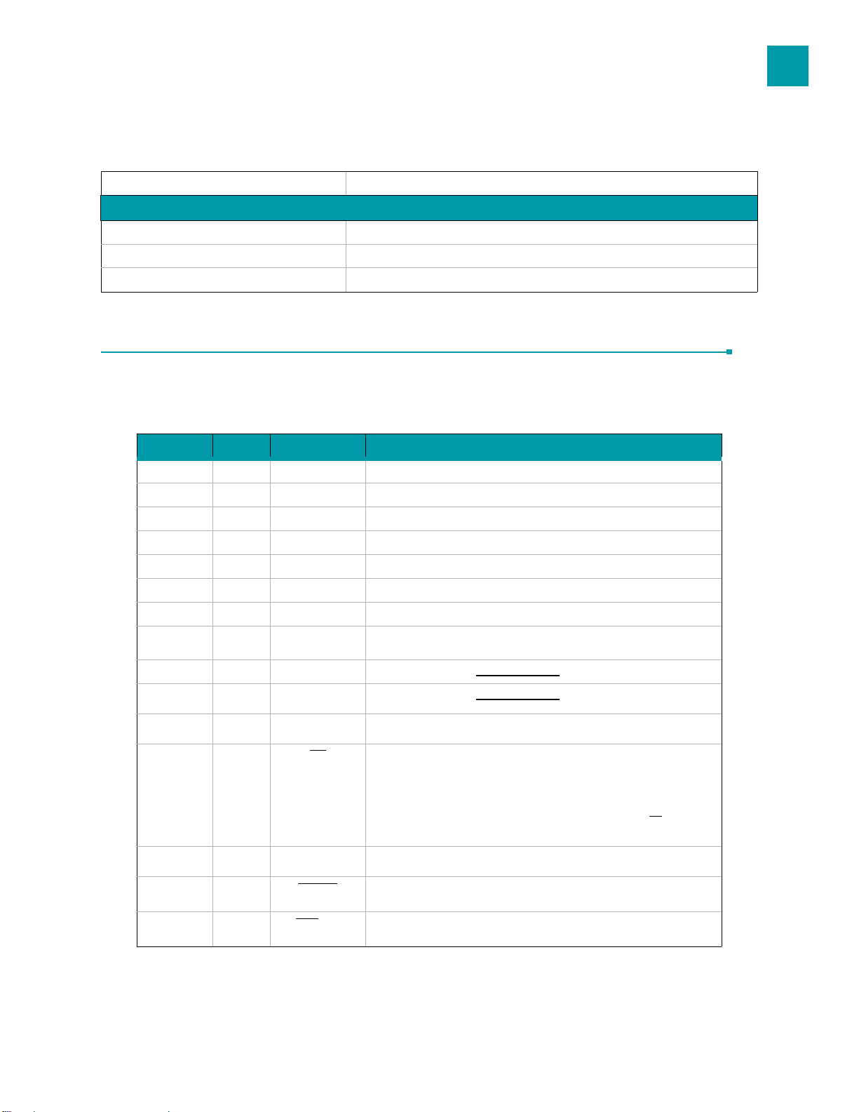
LT2510 User’s Manual
SPECIFICATIONS
Table 1: LT2510 Detailed Specifications
Certifications
FCC Part 15.247 KQL-2510100
Industry Canada (IC) 2268C-2510100
CE Pending
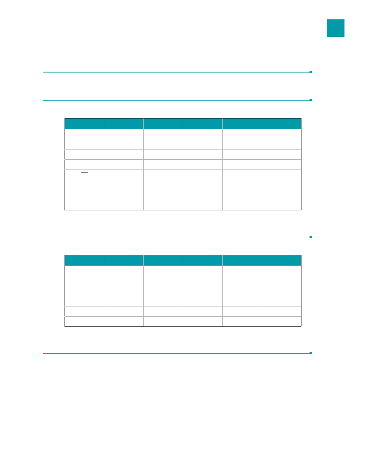
PIN DEFINITIONS
The LT2510 has a simple interface that allows OEM Host communications with the transceiver. Table 2 below shows the
connector pin numbers and associated functions.
Table 2: Pin Definitions for the LT2510 transceiver
SMT Pin Type Signal Name Function
3
1 O GO_0 Generic Output
2 O GO_1 Generic Output
3 DNC Do not connect.
4 Reserved for future use
5 O PWM_Output PWM Digital to Analog Output
6 I RXD Asynchronous serial data input to transceiver
7 O TXD Asynchronous serial data output from transceiver
8 GND GND Signal Ground
9 PWR VCC 3.3 - 3.6 V ±50mV ripple (must be connected)
10 PWR VPA 3.3 - 3.6 V ±50mV ripple (must be connected)
11 GND GND Signal Ground
12 I Test Test Mode – When pulled logic Low and then applying power or resetting, the trans-
13 Reserved Reserved for future use
ceiver’s serial interface is forced to a 9600, 8-N-1 rate. To exit Test mode, the transceiver must be reset or power-cycled with Test Mode pulled logic High or left
floating/disconnected.
Note: Because this mode disables some modes of operation, it should not
nently pulled Low during normal operation.
be perma-
14 I UP_Reset RESET – Controlled by the LT2510 for power-on reset if left unconnected. After a sta-
15 I CMD/Data When logic Low, the transceiver interprets OEM Host data as command data. When
ble power-on reset, a logic Low pulse will reset the transceiver.
logic High, the transceiver interprets OEM Host data as transmit data.
LAIRD TECHNOLOGIES www.lairdtech.com

SPECIFICATIONS
4
Table 2: Pin Definitions for the LT2510 transceiver
SMT Pin Type Signal Name Function
16 O In Range When logic low, the client is in range and synchronized with a server. This will
17 I RTS Request to Send. Floats high if left unconnected, be careful when using enable RTS in
18 O CTS Clear to Send - Active Low when the transceiver is ready to accept data for transmis-
19 Reserved Reserved for future usu. Do not connect.
20 Reserved Reserved for future use. Do not connect.
21 Reserved Reserved for future use. Do not connect.
22 I AD_In Analog to Digital Input
always be low on a Server.
the configuration.
sion.
ENGINEER’S TIP
Design Notes:
• All I/O is 3.3V TTL.
• All inputs are weakly pulled High via a 20kOhm pull-up resistor and may be left floating during
normal operation
• Minimum Connections: VCC, VPA, GND, TXD, & RXD
• Signal direction is with respect to the transceiver
• Unused pins should be left disconnected
LT2510 User’s Manual
ELECTRICAL SPECIFICATIONS
Table 3: Input Characteristics
Signal Name High Min High Max Low Min Low Max Unit
RXD 2.31 3.3 0 .99 V
Test 2.31 3.3 0 .99 V
UP_Reset 0.8 3.3 0 0.6 V
CMD/Data 2.31 3.3 0 .99 V
RTS 2.31 3.3 0 .99 V
AD/_In N/A 3.3 0 N/A V
GI_0 2.31 3.3 0 .99 V
GI_1 2.31 3.3 0 .99 V
SPECIFICATIONS
5
Table 4: Output Characteristics
Signal Name High Min Hiigh Max Low M in Low Max Units
GO_0 2.5 3.3 0 0.4 V
GO_1 2.5 3.3 0 0.4 V
PWM_Output N/A 3.3 0 N/A V
TXD 2.5 3.3 0 0.4 V
In_Range 2.5 3.3 0 0.4 V
CTS 2.5 3.3 0 0.4 V
BLOCK DIAGRAM
Figure 1 includes a functional Block Diagram of the transceiver module.
LAIRD TECHNOLOGIES www.lairdtech.com
 Loading...