AEGIS A5N:300.XXH Service Manual

AEGIS
SEMICONDUTORES LTDA.
VOLTAGE RATINGS
Part Number
A5N:300.12H 1200 1200 1300
A5N:300.14H 1400 1400 1500
A5N:300.16H 1600 1600 1700
A5N:300.18H 1800 1800 1900
A5N:300.20H 2000 2000 2100
A5N:300.XXH
V
, VR (V)
RRM
Max. rep. peak reverse voltage
TJ = 0 to 125 C
O
TJ = -40 to 0 C
V
, VR (V) Max. non-
RSM
rep. peak reverse voltage
O
TJ = 25 to 125 C
O
MAXIMUM ALLOWABLE RATINGS
PARAMETER
TJ Junction Temperature
T
Storage Temperature
stg
I
T(AV)
I
T(RMS)
Max. Av. current 300 A
@ Max. T
C
Nom. RMS current -
VALUE UNITS
-40 to 125 C
-40 to 150 C
75 C
O
O
O
470 A
O
180 half sine wave
4.53 50 Hz half cycle sine wave
I
Max. Peak non-rep. surge
TSM
current
4.94 60 Hz half cycle sine wave
kA
5.23 50 Hz half cycle sine wave
5.70 60 Hz half cycle sine wave
109 t = 10ms
119 t = 8.3 ms
I2t Max. I2t capability kA2s
125 t = 10ms
136 t = 8.3 ms
1/2
I2t
di/dt Max. Non-repetitive rate-ofrise current
PGM Max. Peak gate power
P
G(AV)
+IGM Max. Peak gate current
-VGM Max. Peak negative gate
voltage
F Mounting Force -
1/2
Max. I2t
capability
Max. Av. gate power
1490
800
kA2s
A/ms
10 W
3 W
150 mA
2 V
450 N.m
Initial TJ = 125 C, no voltage applied after surge.
1/2
I2t for time tx = I2t
TJ = 125 C, VD = V
10ms, 0.5ms rise time, Max. repetitive di/dt is aproximately
40% of non-repetitive value.
tp < 5 ms
tp < 5 ms
O
1/2
O
NOTES
1/2
* t
. (0.1 < tx < 10ms).
x
, ITM = 1600A. Gate pulse: 20V, 20 W,
DRM
-
-
Initial TJ = 125 C, rated V
O
applied after surge.
Initial TJ = 125 C, no voltage
O
applied after surge.
Initial TJ = 125 C, rated V
O
applied after surge.
Initial TJ = 125 C, no voltage
O
applied after surge.
-
-
RRM
RRM

AEGIS
0 100 200 300
70
75
80
85
90
95
100
105
110
115
120
125
180º
120º
90º
60º
30º
*Sinusoidal wavefor m
Maximum Allowable Case Temperature
Maximum Allowable Case Temperature (ºC)
Average Forward Current (A)
0 100 200 300 400
70
75
80
85
90
95
100
105
110
115
120
125
DC
180º
120º
90º
60º
30º
*Rectangular wavefor m
Maximum Allowable Case Temperature
Maximum Allowable Case Temperature (ºC)
Average Forward Current (A)
SEMICONDUTORES LTDA.
A5N:300.XXH
CHARACTERISTICS
PARAMETER MIN. TYP. MAX. UNITS
VTM peak on-state voltage
V
Threshold voltage
T(TO)
rT Slope resistance
--- --- 1.93 V
--- --- 0.88
--- ---
1.28
TEST CONDITIONS
Initial TJ = 25 C, 50-60Hz half sine, I
TJ = 125 C
V
Av. power = V
Use low values for ITM < p rated I
mW
O
O
* I
T(TO)
T(AV)
+rT * [I
= 924A.
peak
]2, 180 Half Sine.
T(RMS)
T(AV)
O
IL Latching current
IH Holding current
td Delay time
tq Turn-off time
dv/dt Critical rate-of-rise of
off-state voltage
IRM, IDM Peak reverse and offstate current
IGT DC gate current to trigger
VGT DC gate voltage to
trigger
VGD DC gate voltage not to
trigger
R
Thermal resistance,
thJC
junction-to-case
R
Thermal resistance,
thCS
case-to-sink
wt Weight
--- --- 400 mA
--- ---
--- 0.7 1
--- --- 100
--- --- 1000
500
mA
ms
ms
V/ms
--- 15 30 mA
--- --- 360
--- --- 180
6 --- ---
3 --- ---
mA
V
--- --- 0.3 V
---
O
O
O
O
g(oz.)
--- --- 0.085 C/W
--- --- 0.106 C/W
--- --- 0.109 C/W
--- --- 0.03 C/W
---
57(2.1)
Case Style JEDEC
TC = 125 C, 12V anode. Gate pulse: 10V, 20W, 100ms.
TC = 25 C, 12V anode. Initial IT = 15A.
TC = 25 C, VD = V
20W, 10ms, 1ms rise time.
TJ = 125 C, ITM = 550A, di/dt = 40A/ms, VR = 50V. dv/dt = 20
V/ms lin. to rated V
TJ = 125 C, Exp. To 67% V
TJ = 125 C, Rated V
TC = -40 C
TC = 25 C
TC = -40 C
TC = 25 C
TC = 25 C, Max. Value which will not trigger with rated V
O
O
O
O
O
O
O
O
O
O
O
, 50A resistive load. Gate pulse: 10V,
DRM
. Gate: 0V, 100 W.
DRM
, gate open.
DRM
RRM
and V
, gate open.
DRM
+12V anode-to-cathode. For recommended
gate drive see "Gate Characteristics" figure.
DRM
anode.
DC operation, double side cooled.
O
180 sine wave, double side cooled.
O
120 rectangular wave, double side cooled.
Mtg. Surface smooth, flat and greased. Double side cooled.
---
---TO-200AA
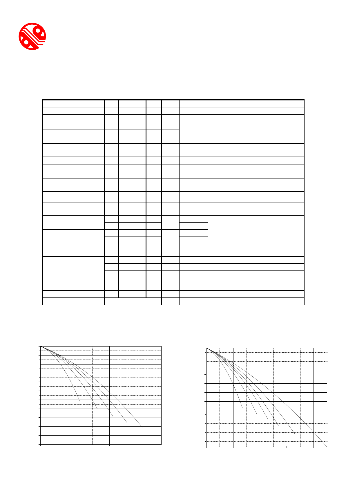
Fig. 1 - Current Ratings Characteristics
Fig. 2 - Current Ratings Characteristics
 Loading...