AEGIS
SEMICONDUTORES LTDA.
A5N:1000.XXH
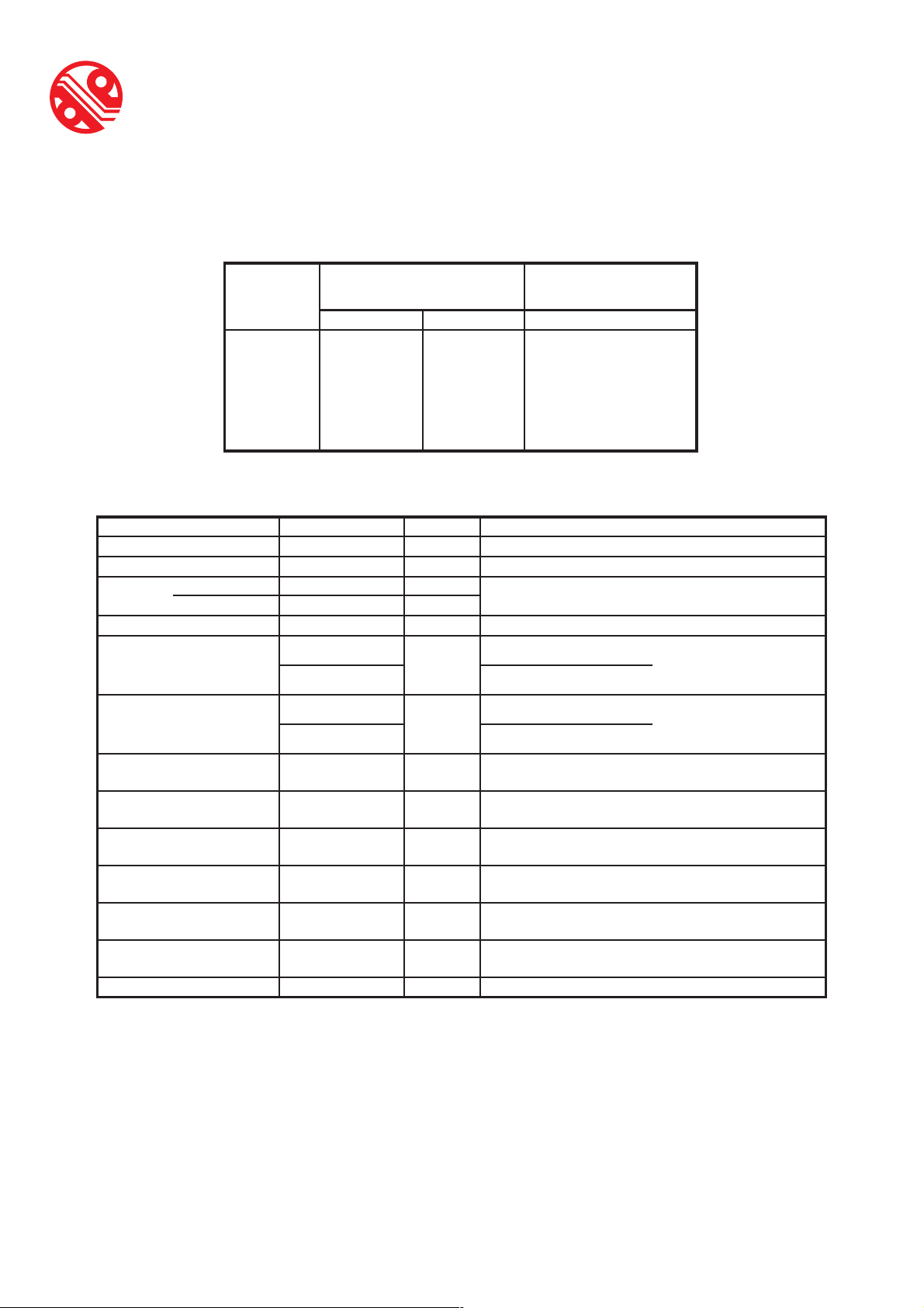
VOLTAGE RATINGS
V
, VR – (V) Max.
RRM
Part Number
rep. peak reverse voltage
T
=0to125C
J
O
= -40 to 0 C TJ=25to125C
T
J
A5N:1000.22H 2200 2200 2300
A5N:1000.24H 2400 2400 2500
A5N:1000.26H 2600 2600 2700
A5N:1000.28H 2800 2800 2900
A5N:1000.30H 3000 3000 3100
A5N:1000.32H 3200 3200 3300
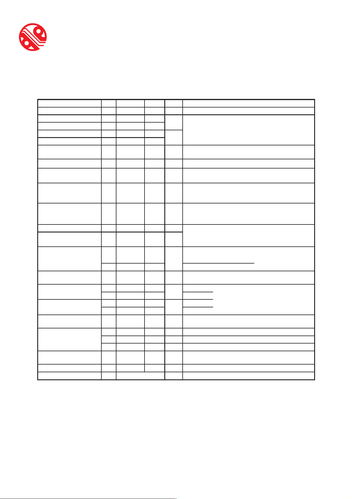
MAXIMUM ALLOWABLE RATINGS
PARAMETER
T
Junction Temperature
J
T
Storage Temperature
stg
I
T(AV)
I
T(RMS)
I
Max. Peak non-rep. surge
TSM
Max. Av. current 1000 A
@ Max. T
C
Nom. RMS current -
current
VALUE UNITS
-40 to 125 C
-40 to 150 C
74 C
O
O
O
1600 A
14000 50 Hz half cycle sine wave
A
15000 60 Hz half cycle sine wave
V
RSM,VR
rep. peak reverse voltage
O
O
180 half sine wave
– (V) Max. non-
O
NOTES
-
-
Initial T
applied after surge.
O
= 125 C, rated V
J
RRM
2
t Max. I2t capability
I
2t1/2
I
Max. I2t
1/2
capability
di/dt Max. Non-repetitive rate-ofrise current
P
M Max. Peak gate power
G
P
Max. Av. gate power
G(AV)
Max. Peak gate current
+I
GM
Max. Peak negative gate
-V
GM
voltage
F Mounting Force
937000
2
s
A
973000
46700
300
200
5
10
5
kA
A/ms
2s1/2
W
W
A
V
24500(5500) +- 10% N(Lbf)
t = 10ms
Initial T
applied after surge.
t = 8.3 ms
Initial T
2
I
t for time tx=I2t
= 125 C, VD=V
T
J
O
= 125 C, no voltage applied after surge.
J
O
1/2
1/2
*t
. (0.1 < tx < 10ms).
x
DRM,ITM
= 3000A. Gate pulse: 20V, 20 W,
apriximately 40% of non-repetitive value.
tp=40ms
-
-
-
-
O
= 125 C, rated V
J
O
O
RRM

AEGIS
SEMICONDUTORES LTDA.
A5N:1000.XXH
CHARACTERISTICS
PARAMETER MIN. TYP. MAX. UNITS
V
peak on-state voltage --- --- 2.26 V
TM
V
Low-level threshold --- --- 1.31
F(TO)1
High-level threshold --- --- 1.55
V
F(TO)2
r
Low-level resistance --- --- 0.48
T1
r
High-level resistance --- --- 0.38
T2
I
Latching current
L
I
Holding current --- ---
H
Delay time
t
d
Turn-off time
t
q
--- --- 800 mA
400
--- 0.7 1.5
--- 125 250
O
= 25 C, 50-60Hz half sine, I
Initial T
J
O
T
= 125 C
J
V
Av. power = V
Use low values for I
mW
T
= 125 C, 12V anode. Gate pulse: 10V, 20W, 100ms.
C
= 25 C, 12V anode. Initial IT = 15A.
T
C
mA
T
=25C,VD= rated V
C
ms
10V, 20W,20ms, 0.1ms rise time.
= 125 C, ITM= 1000A, di/dt = 25A/ms, VR= -50V. dv/dt = 20
T
J
ms
V/ms lin. To 80% rated V
T(TO)*IT(AV)+rT
O
O
O
O
TEST CONDITIONS
= 3000A.
peak
*[I
]2, 180 Half Sine.
T(RMS)
< p rated I
TM
DRM
T(AV)
, 50A resistive load. Gate pulse:
. Gate: 0V, 100W.
DRM
t
Turn-off time with
q(diode)
feedback diode
I
Recovery current
RM(REC)
Recovered charge
Q
RR
dv/dt Critical rate-of-rise of offstate voltage
--- --- 50
--- 93 --- A
--- 166 ---
300 --- 1000
ms
mC
V/ms
--- --- 300
Peak reverse and off-
I
RM,IDM
state current
I
DC gate current to trigger
GT
DC gate voltage to trigger
V
GT
V
DC gate voltage not to
GD
trigger
R
Thermal resistance,
thJC
junction-to-case
R
Thermal resistance,
thCS
case-to-sink
wt Weight
Case Style --- JEDEC
--- 15 75 mA
--- 40 300
--- 20 150
0.3 --- 5
0.3 --- 3
mA
V
--- --- 0.200 V
---
O
O
O
O
g(oz.)
--- --- 0.025 C/W
--- --- 0.025 C/W
--- --- 0.027 C/W
--- --- 0.010 C/W
---
460(16.0)
TO-200AD
O
T
= 125 C, ITM= 1000A, di/dt = 25A/ms, VR= 1V. dv/dt = 600
J
V/ms lin. To 40% rated V
O
TJ= 125 C, ITM= 1000A, diR/dt = 25A/ms.
O
T
= 125 C. Exp. to 100% or lin.
J
To 80% V
T
= 125 C, Exp. To 67% V
J
T
= 125 C, Rated V
J
= -40 C
T
C
=25C
T
C
= -40 C
T
C
=25C
T
C
T
= 25 C, Max. Value which will not trigger with rated V
C
, gate open.
DRM
O
O
O
O
+6V anode-to-cathode. For recommended gate
O
drive see "Gate Characteristics" figure.
O
O
. Gate: 0V, 100W.
DRM
DRM
and V
RRM
Higher dv/dt values
avaliable.
, gate open.
, gate open.
DRM
DRM
anode-to-cathode.
DC operation, double side cooled.
O
180 sine wave, double side coolde.
O
120 rectangular wave, double side cooled.
Mtg. Surface smooth, flat and greased. Single side cooled. For
double side, divide by 2.
---
---
 Loading...