

Page 1

Copyright
This documentation and the software included with this product are
copyrighted 2002 by Advantech Co., Ltd. All rights are reserved.
Advantech Co., Ltd. reserves the right to make improvements in the
products described in this manual at any time without notice. No part of this
manual may be reproduced, copied, translated or transmitted in any form or
by any means without the prior written permission of Advantech Co., Ltd.
Information provided in this manual is intended to be accurate and reliable.
However, Advantech Co., Ltd. assumes no responsibility for its use, nor for
any infringements of the rights of third parties which may result from its
use.
Acknowledgments
PC-LabCard is a trademark of Advantech Co., Ltd. IBM and PC are
trademarks of International Business Machines Corporation. MS-DOS,
Windows, Microsoft Visual C++ and Visual BASIC are trademarks of
Microsoft Corporation. Intel and Pentium are trademarks of Intel
Corporation. Delphi and C++ Builder are trademarks of Inprise
Corporation.
CE notification
The PCI-1784, developed by ADVANTECH CO., LTD., has passed the CE
test for environmental specifications when shielded cables are used for
external wiring. We recommend the use of shielded cables. This kind of
cable is available from Advantech. Please contact your local supplier for
ordering information.
On-line Technical Support
For technical support and service, please visit our support website at:
http://www.advantech.com/support
Note:
✎ Concerning the environment protection, we’d like to reduce the paper
using for the user’s manual. Starting the page of Appendix C, please find
the PDF file of the CD-ROM.
Part No. 2003178400 1st Edition
Printed in Taiwan July 2002
1
Page 2

2
Page 3

Contents
1. INTRODUCTION.................................................................................................................. 1
1.1
FEATURES
1.2 A
PPLICATIONS
1.3 I
NST AL LATION GUIDE
1.4 S
OFTWARE OVERVIEW
1.5 D
EVICE DRIVERS PROGRAMMING ROADMAP
1.6 A
CCESSORIES
........................................................................................................................1
.................................................................................................................4
......................................................................................................4
.....................................................................................................6
..................................................................7
..................................................................................................................9
2. INSTALLATION.................................................................................................................. 10
2.1 U
NP ACKING
2.2 D
RIVER INSTALLATION
2.3 H
ARDWARE INST ALLATION
2.4 D
EVICE SETUP
...................................................................................................................10
..................................................................................................12
............................................................................................13
& C
ONFIGURATION
................................................................................16
3. SIGNAL CONNECTIONS.................................................................................................. 19
3.1
OVERVIEW
3.2 S
WITCH AND JUMPER SETTINGS
3.3 S
IGNAL CONNECTIONS
.....................................................................................................................19
....................................................................................19
..................................................................................................21
APPENDIX A. SPECIFICAT IONS........................................................................................ 25
APPENDIX B. BLOCK DIAGRAM......................................................................................27
APPENDIX C. REGISTER STRUCTURE AND FORMAT............................................... 29
C.1 O
VERVIEW
C.2 I/O P
C.3 C
C.4 C
C.5 C
C.6 I
C.7 I
C.8 C
C.9 C
OUNTER
OUNTER
OUNTER
NTERRUPT CONTROL REGISTER
NTERRUPT STATUS REGISTER
LEAR INTERRUPT
LEAR INTERRUPT
....................................................................................................................29
ORT ADDRESS MAP
0/1/2/3
0/1/2/3
0/1/2/3
..............................................................................................29
— BASE+00/04/08/0CH ...................................................... 33
MODE
LATCH DATA
COMPARE DATA
— BASE+00/04/08/0CH.............................................35
— BASE+10/14/18/1CH........................................ 36
— BASE+20H........................................................... 37
— BASE+20H .............................................................. 38
— BASE+24H............................................................................... 39
— BASE+24H............................................................................... 40
3
Page 4

C.10 S
OFTWARE LATCH
— BASE+28H.............................................................................. 41
C.11 B
C.12 R
C.13 D
C.14 D
ID — BASE+28H..........................................................................................42
OARD
ESET COUNTER
IGITAL OUTPUT
IGITAL INPUT/OUTPUT
— BASE+2CH................................................................................ 43
— BASE+30H................................................................................ 44
— BASE+30H ..................................................................... 45
APPENDIX D. OPERATION ................................................................................................. 47
D.1 Q
D.2 C
D.3 D
D.4 L
D.5 C
D.6 T
D.7 I
UADRATURE ENCODER INTRODUCTION
OUNTER MODES
IGITAL NOISE FILTER
ATCH MODE
OUNTER RESET VALUE
IMER FUNCTION
NTERRUPT FUNCTION
.........................................................................................................48
..................................................................................................49
................................................................................................................50
................................................................................................51
..........................................................................................................51
..................................................................................................52
......................................................................47
4
Page 5

1. Introduction
Thank you for buying the Advantech PCI-1784. The PCI-1784 is a 4axis quadrature encoder and counter card for PCI bus. This card
includes four 32-bit quadruple AB phase encoder counters, 8-bit timer
with multi range time-base selector and four isolated digital input and
four isolated digital output. Its flexible interrupt sources are suitable for
motor control and position monitoring.
The following sections of this chapter will provide further information
about features of the multifunction cards, a Quick Start for installation,
together with some brief information on software and accessories for the
PCI-1784 card.
1.1 Features
❏ Four 32-bit up/down counters
❏ Single ended or differential inputs
❏ Pulse/direction and up/down counter
❏ x1, x2, x4 counts for each encoder cycle
❏ Optically isolated up to 2500 V
DC
❏ 4-stage digital filter with selectable sampling rate
❏ On board 8-bit timer with wide range time-base selector
❏ Multiple interrupt sources for precision application
❏ Four isolated digital input
❏ Four isolated digital output with flexible function
❏ Board ID
The Advantech PCI-1784 offers the following main features:
Encoder Interface
Each channel includes a decoding circuit for incremental quadrature
encoding. Inputs accept either single-ended or differential signals.
Quadrature input works with or without an index, allowing linear or
rotary encoder feedback.
1
Page 6

Counters
The PCI-1784 has four independent 32-bit counters. The maximum
quadrature input rate is 2 MHz, and the maximum input rate in counter
mode is 8 MHz. You can individually configure each counter for
quadrature decoding, pulse/direction counting or up/down counting.
Digital Input and Interrupts
The PCI-1784 provides four digital input channels. Each channel
accepts digital input as an index input for a rotary encoder or as a home
sensor input for a linear encoder. The card can generate an interrupt to
the system based on a signal from its digital inputs, overflow/underflow
and over-compare/under-compare of its counters, or on a programmed
time interval. It can repeatedly generate interrupts at any time interval
you specify, from 20 micro second to 51 second. These interrupts let
you precisely monitor the speed of a control system.
Flexible Digital Output function
The PCI-1784 provides four digital output channels. Each channel
accepts digital output as a normal TTL output for a rotary encoder, or as
an indicated output with pulse/level mode for a linear encoder. The PCI1784 can generate an indicated output based on a signal from overcompare/under-compare of its counters. The pulse width of an indicated
output is depends on the counter clock or clear interrupt.
Special Shielded Cable for Noise Reduction
The PCL-10137H shielded cable is specially designed for the PCI-1784
for reducing noise. Its wires are all twisted pairs, and the input signals
and output signals are separately shielded, providing minimal cross talk
between signals and the best protection against EMI/EMC problems.
Keeping the Counter Values and the Output Status after system
reset
Users can independently use the four counter channels. When the
system is hot reset (power not shut down), the PCI-1784 can either
retain the last counter values and the output status, or return to its
2
Page 7

default configuration, depending on jumper setting. This practical
function eliminates danger caused by miss-operation during unexpected
system reset.
Board ID
The PCI-1784 has a built-in DIP Switch that helps define each card’s ID
when multiple PCI-1784 cards have been installed on the same PC
chassis. The board ID setting function is very useful when users build
their system with multiple PCI-1784 cards. With correct Board ID
settings, you can easily identify and access each card during hardware
configuration and software programming.
Note:
✎ For detailed specifications of the PCI-1784, please refer to Appendix A,
Specifications.
3
Page 8

1.2 Applications
❏
Motion control
❏
Position sensing, monitoring and measuring
❏
Coordinate measuring machines
❏
X-Y table monitors
❏
Robotics
❏
Machine control
1.3 Installation Guide
Before you install your PCI-1784 card, please make sure you have the
following necessary components:
❏
PCI-1784 DA&C card
❏
PCI-1784 User’s Manual
❏
Driver software Advantech DLL drivers
❏
Wiring cable PCL-10137H (option)
(included in the companion CD-ROM)
❏
Wiring board ADAM-3937 (option)
❏
Computer Personal computer or workstation with a
PCI-bus slot (running Windows 2000/95/98/
NT/ME/XP)
Some other optional components are also available for enhanced
operation:
❏
Application software ActiveDAQ, GeniDAQ or other third-party
software packages
After you get the necessary components and maybe some of the
accessories for enhanced operation of your Multifunction card, you can
then begin the Installation procedures. Figure 1-1 on the next page
provides a concise flow chart to give users a broad picture of the
software and hardware installation procedures:
4
Page 9
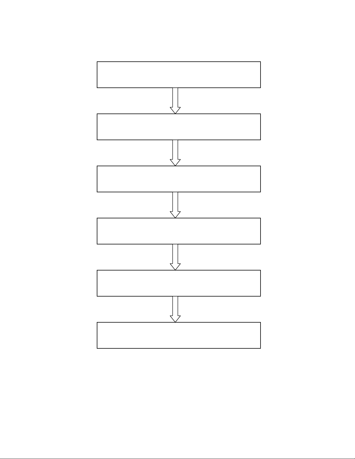
Install Driver from CD-ROM, then power-off P C
Install Hardware and power-on PC
Use driver utility to configure hardware
Use test utility to test hardware
Read examples & driver manual
Start to write your own application
Fig. 1-1 Installation Flow Chart
5
Page 10

1.4 Software Overview
Advantech offers a rich set of DLL drivers, third-party driver support
and application software to help fully exploit the functions of your PCI1784 card:
❏
Device Drivers (on the companion CD-ROM)
❏
LabVIEW driver*
❏
Advantech ActiveDAQ
❏
Advantech GeniDAQ
Programming choices for DA&C cards: You may use Advantech
application software such as Advantech Device Drivers. On the other
hand, advanced users are allowed another option for register-level
programming, although not recommended due to its laborious and timeconsuming nature.
Device Drivers
The Advantech Device Drivers software is included on the companion
CD-ROM at no extra charge. It also comes with all the Advantech
DA&C cards. Advantech’s device drivers features a complete I/O
function library to help boost your application performance. The
Advantech Device Drivers for Windows 2000/95/98/ ME/NT/XP
works seamlessly with development tools such as Visual C++, Visual
Basic, Inprise C++ Builder and Inprise Delphi.
Register-level Programming
Register-level programming is reserved for experienced programmers
who find it necessary to write codes directly at the level of device
registers. Since register-level programming requires much effort and
time, we recommend that you use the Advantech Device Drivers
instead. However, if register-level programming is indispensable, you
should refer to the relevant information in Appendix C, Register
Structure and Format, or to the example codes included on the
companion CD-ROM.
6
Page 11

1.5 Device Drivers Programming Roadmap
This section will provide you a roadmap to demonstrate how to build
an application from scratch using Advantech Device Drivers with your
favorite development tools such as Visual C++, Visual Basic, Delphi
and C++ Builder. The step-by-step instructions on how to build your
own applications using each development tool will be given in the
Device Drivers Manual. Moreover, a rich set of example source codes
are also given for your reference.
Programming Tools
Programmers can develop application programs with their favorite
development tools:
❏
Visual C++
❏
Visual Basic
❏
Delphi
❏
C++ Builder
For instructions on how to begin programming works in each
development tool, Advantech offers a Tutorial Chapter in the Device
Drivers Manual for your reference. Please refer to the corresponding
sections in this chapter on the Device Drivers Manual to begin your
programming efforts. You can also take a look at the example source
codes provided for each programming tool, since they can get you very
well-oriented.
The Device Drivers Manual can be found on the companion CD-ROM.
Or if you have already installed the Device Drivers on your system,
The Device Drivers Manual can be readily accessed through the Start
button:
Start/Programs/Advantech Driver V2.0/Device Driver Manual
The example source codes could be found under the corresponding
installation folder such as the default installation path:
\Program Files\Advantech\ADSAPI\Example s
7
Page 12

For information about using other function groups or other
development tools, please refer to the Creating Windows 95/NT/2000
Application with Device Drivers chapter and the Function Overview
chapter on the Device Drivers Manual.
Programming with Device Drivers Function Library
Advantech Device Drivers offers a rich function library to be utilized
in various application programs. This function library consists of
numerous APIs that support many development tools, such as Visual
C++, Visual Basic, Delphi and C++ Builder.
According to their specific functions or services, those APIs can be
categorized into several function groups:
❏
Digital Input/Output Function Group
❏
Counter Function Group
❏
Port Function Group (direct I/O)
❏
Event Function Group
For the usage and parameters of each function, please refer to the
Function Overview chapter in the Device Drivers Manual.
Troubleshooting Device Drivers Error
Driver functions will return a status code when they are called to
perform a certain task for the application. When a function returns a
code that is not zero, it means the function has failed to perform its
designated function. To troubleshoot the Device Drivers error, you can
pass the error code to DRV_GetErrorMessage function to return the
error message. Or you can refer to the Device Drivers Error Codes
Appendix in the Device Drivers Manaul for a detailed listing of the
Error Code, Error ID and the Error Message.
8
Page 13

1.6 Accessories
Advantech offers a complete set of accessory products to support the
PCI-1784 card. These accessories include:
Wiring Cable
❏
PCL-10137H The PCL-10137H shielded cable is specially designed
Wiring Boards
❏
ADAM-3937 The ADAM-3937 is a 37-pin D-type wiring terminal
for PCI-1784 cards to provide high resistance to noise.
To achieve a better signal quality, the signal wires are
twisted in such a way as to form a “twisted-pair cable”,
reducing cross-talk and noise from other signal sources.
Furthermore, its analog and digital lines are separately
sheathed and shielded to neutralize EMI/EMC
problems.
module for DIN-rail mounting. This terminal module
can be readily connected to the Advantech PC-Lab
cards and allow easy yet reliable access to individual
pin connections for the PCI-1784 card.
9
Page 14

2. Installation
This chapter gives users a package item checklist, proper instructions
about unpacking and step-by-step procedures for both driver and card
installation.
2.1 Unpacking
After receiving your PCI-1784 package, please inspect its contents first.
The package should contain the following items:
! PCI-1784 card
! Companion CD-ROM (DLL driver included)
! User’s Manual
The PCI-1784 card harbors certain electronic components vulnerable to
electrostatic discharge (ESD). ESD could easily damage the integrated
circuits and certain components if preventive measures are not carefully
paid attention to.
Before removing the card from the antistatic plastic bag, you should
take following precautions to ward off possible ESD damage:
" Touch the metal part of your computer chassis with your hand to
discharge static electricity accumulated on your body. Or one can
also use a grounding strap.
" Touch the anti-static bag to a metal part of your computer chassis
before opening the bag.
" Take hold of the card only by the metal bracket when removing it
out of the bag.
After taking out the card, first you should:
" Inspect the card for any possible signs of external damage (loose or
damaged components, etc.). If the card is visibly damaged, please
notify our service department or our local sales representative
immediately. Avoid installing a damaged card into your system.
10
Page 15

Also pay extra caution to the following aspects to ensure proper
installation:
! Avoid physical contact with materials that could hold static
electricity such as plastic, vinyl and Styrofoam.
! Whenever you handle the card, grasp it only by its edges. DO NOT
TOUCH the exposed metal pins of the connector or the electronic
components.
Note:
✎ Keep the anti-static bag for future use. You might need the original bag to
store the card if you have to remove the card from PC or transport it
elsewhere.
11
Page 16
2.2 Driver Installation
We recommend you to install the driver before you install the PCI1784 card into your system, since this will guarantee a smooth
installation process.
The Advantech Device Drivers Setup program for the PCI-1784 card is
included on the companion CD-ROM that is shipped with your DA&C
card package. Please follow the steps below to install the driver
software:
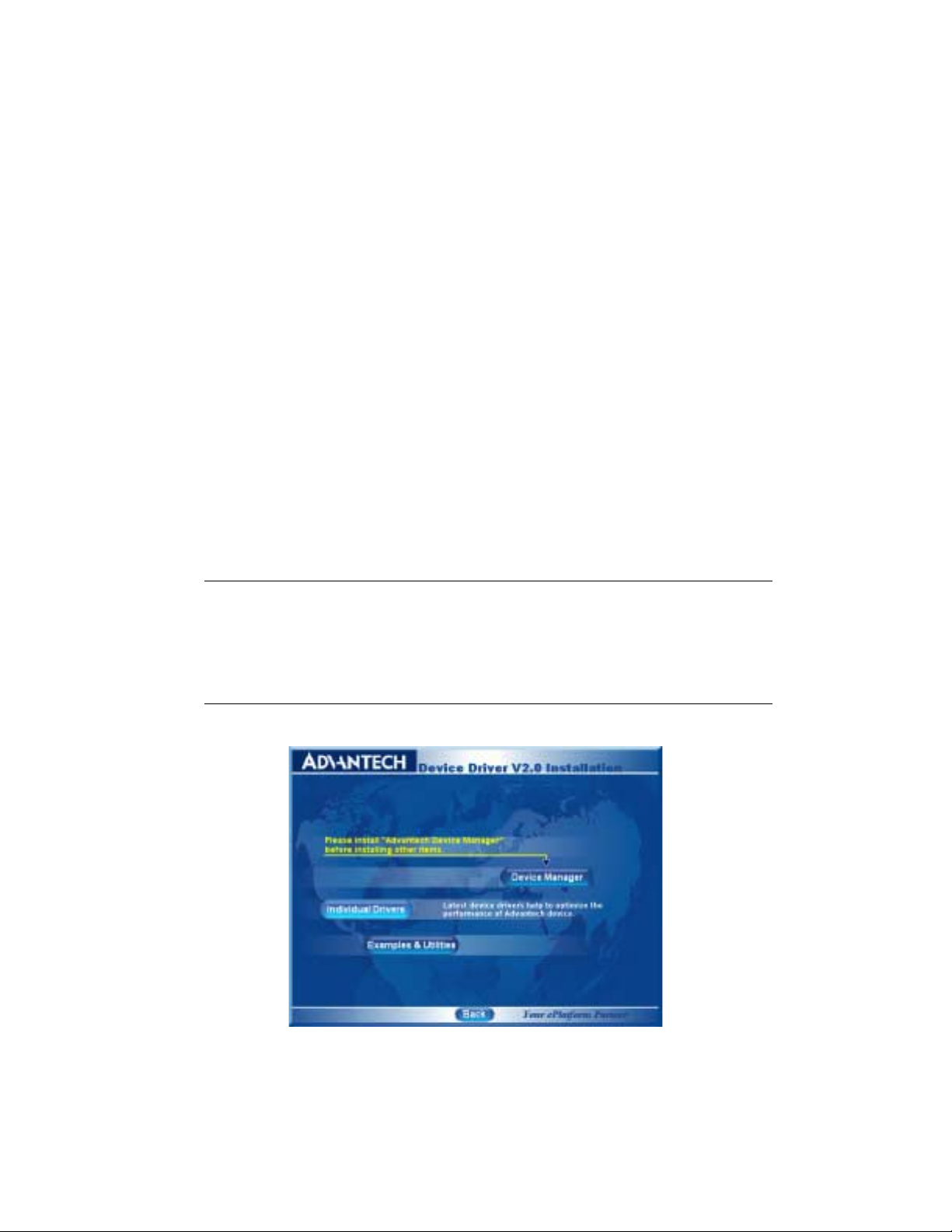
Step 1: Insert the companion CD-ROM into your CD-ROM drive.
Step 2: The Setup program will be launched automatically if you have
the autoplay function enabled on your system. When the Setup
Program is launched, you’ll see the following Setup Screen.
Note:
✎ If the autoplay function is not enabled on your computer, use Windows
Explorer or Windows Run command to execute SETUP.EXE on the
companion CD-ROM.
Fig. 2-1 The Setup Screen of Advantech Automation Software
12
Page 17
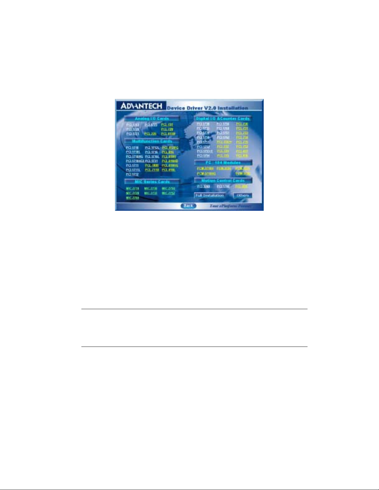
Step 3: Select the Individual Drivers option.
Step 4: Select the specific device then just follow the installation
instructions step by step to complete your device driver setup.
Fig. 2-2 Different options for Driver Setup
For further information on driver-related issues, an online version of
Device Drivers Manual is available by accessing the following path:
Start/Programs/Advantech Device Drivers V2.0/Device Driver Manual
2.3 Hardware Installation
Note:
✎ Make sure you have installed the driver first before you install the card
(please refer to 2.2 Driver Installation)
After the DLL driver installation is completed, you can now go on to
install the PCI-1784 card in any PCI slot on your computer. But it is
suggested that you should refer to the computer user manual or related
documentation if you have any doubt. Please follow the steps below to
install the card on your system.
13
Page 18

Step 1: Turn off your computer and unplug the power cord and cables.
TURN OFF your computer before installing or removing any
components on the computer.
Step 2: Remove the cover of your computer.
Step 3: Remove the slot cover on the back panel of your computer.
Step 4: Touch the metal part on the surface of your computer to
neutralize the static electricity that might be on your body.
Step 5: Insert the PCI-1784 card into a PCI slot. Hold the card only by
its edges and carefully align it with the slot. Insert the card
firmly into place. Use of excessive force must be avoided,
otherwise the card might be damaged.
Step 6: Fasten the bracket of the PCI card on the back panel rail of the
computer with screws.
Step 7: Connect appropriate accessories (37-pin cable, wiring terminals,
etc. if necessary) to the PCI card.
Step 8: Replace the cover of your computer chassis. Re-connect the
cables you removed in step 2.
Step 9: Plug in the power cord and turn on the computer.
Note:
✎ In case you installed the card without installing the DLL driver first,
Windows 95/98/ME will recognize your card as an “unknown device” after
rebooting, and will prompt you to provide the necessary driver. You should
ignore the prompting messages (just click the Cancel button) and set up the
driver according to the steps described in 2.2 Driver Installation.
After the PCI-1784 card is installed, you can verify whether it is
properly installed on your system in the Device Manager:
1. Access the Device Manager through Control Panel/System/Device
Manager.
2. The device name of the PCI-1784 should be listed on the Device
Manager tab on the System Property Page.
14
Page 19

Fig. 2-3 The device name listed on the Device Manager
Note:
✎ If your card is properly installed, you should see the device name of your
card listed on the Device Manager tab. If you do see your device name
listed on it but marked with an exclamation sign “!”, it means your
card has not been correctly installed. In this case, remove the card
device from the Device Manager by selecting its device name and press
the Remove button. Then go through the driver installation process
again.
After your card is properly installed on your system, you can now
configure your device using the PCI-1784 Utility program that has itself
already been installed on your system during driver setup. A complete
device installation procedure should include board selection and device
setup. After that, you can operate this card through the operation. The
following sections will guide you through the board selection, device
setup and operation of your device.
15
Page 20

2.4 Device Setup & Configuration
The PCI-1784 Utility program is a utility that allows you to setup,
configure and test your device, and later stores your settings on the
system registry. These settings will be used when you call the APIs of
Advantech Device Drivers.
Board selection
After your card is properly inserted, the Windows system will install the
drivers properly. You just need to launch the PCI-1784 Utility for board
selection. Click Board Selection and the board dialog box will appear
as seen below (Fig. 2-4):
Fig. 2-4 The ‘Board Selection’ dialog box
16
Page 21

Setting Up and configure the device
Click Setup to configure each parameter. The dialog box will appear as
seen below (Fig. 2-5):
Fig. 2-5 The ‘Setup’ dialog box
17
Page 22

Fig. 2-6 The “Operation” dialog box
After your card is properly installed and configured, you can click the
Operation button to test your hardware. For more detailed information,
please refer to Chapter 2 of the Device Drivers Manual.
You can also find the rich examples on the CD-ROM to speeding up
your programming.
18
Page 23

3. Signal Connections
3.1 Overview
Maintaining signal connections is one of the most important factors in
ensuring that your application system is sending and receiving data
correctly. A good signal connection can avoid unnecessary and costly
damage to your PC and other hardware devices. This chapter provides
useful information about how to connect input and output signals to the
PCI-1784 via the I/O connector.
3.2 Switch and Jumper Settings
The PCI-1784 card has one function switch and five jumper settings.
Fig. 3-1 Card connector, jumper and switch locations
Table 3-1: Summary of jumper settings
Names of Jumpers Function description
Keep last status after hot reset
JP2
Default configuration
19
Page 24

Setting the time to reset the digital outputs and the counter
value
Some users will want the capability of clearing each counter and the
isolated digital output when the system (or PC) issues a reset signal on
the PCI bus. Some users will want to clear their counter and digital
output only as part of system power-on.
The PCI-1784 satisfies both these needs by providing jumper JP2.
Depending on the application, this capability may allow counter value
and the isolated digital outputs to be "OFF" without requiring a
complete shutdown of processes controlled by the card.
Complete loss of power to the chip clears the chip memory. Thus, no
matter how JP2 is set, if the power to the PCI-1784 is disconnected, the
counter value and the isolated digital output initial power-on state will
be "OFF".
Board ID setting (SW1)
ID3 ID2 ID1 ID0 Board ID
1111 0
1110 1
1101 2
1100 3
1011 4
1010 5
1001 6
1000 7
0111 8
0110 9
0101 10
0100 11
0011 12
0010 13
0001 14
0000 15
Note: On: 1, Off: 0
20
Page 25

3.3 Signal Connections
Pin Assignment
Figure 3-2 shows the pin assignments for the 37-pin I/O connector on
the PCI-1784.
EGND 1 20 CH0ACH0A+ 2 21 CH0BCH0B+ 3 22 CH0Z-
CH0Z+ 4 23 CH1ACH1A+ 5 24 CH1BCH1B+ 6 25 CH1Z-
CH1Z+ 7 26 CH2ACH2A+ 8 27 CH2BCH2B+ 9 28 CH2Z-
CH2Z+ 10 29 CH3ACH3A+ 11 30 CH3BCH3B+ 12 31 CH3Z-
CH3Z+ 13 32 EGND
IDI COM 14 33 IDI1
IDI0 15 34 IDI3
IDI2 16 35 EGND
EGND 17 36 IDO1
IDO0 18 37 IDO3
IDO2 19
.
Fig. 3-2 I/O connector pin assignments for the PCI-1784
I/O Connector Signal Description
Table 3-2 I/O Connector Signal Description
Signal Name Reference Direction Description
EGND - - External Ground.
CH<0..3>A+ EGND Input Channel <0..3> A differential positive-in put .
CH<0..3>A- EGND Input Channel <0..3> A differential negative-input.
CH<0..3>B+ EGND Input Channel <0..3> B differential positive-input.
CH<0..3>B- EGND Input Channel <0..3> B differential negative-input.
CH<0..3>Z+ EGND Input Channel <0..3> Z differential positive-input.
CH<0..3>Z- EGND Input Channel <0..3> Z differential negative-input.
IDI<0..3> I DI COM Input Isolated Digital Input, Channels 0 through 3.
IDI COM - - Common input of the Isolated Digital Input.
IDO<0..3> EGND Output Isolated Digital Output, Channels 0 through 3.
EGND - - External Ground.
21
Page 26

Quadrature encoder input
Single ended
outputs of
Encoder
GND
Differential
outputs of
Encoder or
Line driver
GND
A
B
I
A+
AB+
BI+
I-
CHnA+
CHnB+
CHnZ+
PCI-1784
connector
EGND
CHnA+
CHnA-
CHnB+
CHnB-
CHnZ+
CHnZ-
PCI-1784
connector
EGND
PULSE
DIR
Pulse/Direction
Counter
GND
CHnA+
CHnB+
PCI-1784
connector
EGND
Figure 3-3: Quadrature encoder input connections
22
Page 27

UP
DN
CHnA+
CHnB+
Up/Down
Counter
Two_Pulse
Up Counter
GND
UP
DN
GND
UP
DN
PCI-1784
connector
EGND
CHnA+
CHnB+
PCI-1784
connector
EGND
CHnA+
CHnB+
Two_Pulse
Down Counter
GND
PCI-1784
connector
EGND
Figure 3-4: Quadrature encoder (up/down counter) input connections
Note:
✎ In case you want to connect the Up/Down counter signal into the PCI-1784,
be sure that all the signals must be connected. The floating connection will
cause unexpected result.
23
Page 28

Isolated digital input
IDI0~IDI3
DC
(5-30V)
InternalExternal
VCC
IDI COM
Figure 3-4: Isolated digital input connections
Isolated digital output
TTL
level
Internal
Isolated
Protection
Circuit
GND
External
IDO0~IDO3
TTL
level
EGND
Figure 3-5: Isolated digital output connections
24
Page 29

Appendix A. Specifications
Encoder Output
Number of Axis 4 (independent)
Resolution 32-bit
Max. Quadrature
Input Frequency
Digital Filter 4 stage
Drive Type Single-ended or differential
Counter Mode Quadrature, Up/Down, Count/Direction
Optical Isolation 2500 V
Max. Input Pulse
Frequency
Sample Clock
Frequency
Timer
Resolution 8-bit
Time base 50 K, 5 K, 500, 50, 5 Hz
w/ Digital Filter 1.0 MHz
w/o Digital
Filter
2.0 MHz
DC
x 1, x 2, x 4
8, 4, 2, or 1 MHz
Isolated Digital Input
Number of Channel 4
Optical Isolation 2500 V
Opto-isolator response time
25µs
Over-voltage Protect 70 V
VIH (max.) 30 V
Input Voltage
VIH (min.) 10 V
VIL (max.) 3 V
10 V
DC
12 V
DC
24 V
DC
Isolated Digital Output
Number of Channel 4
Optical Isolation 2500 V
Response time
20 µs (max.)
Supply Vol tag e TTL level
Sink/Source Current 50 mA max./channel
DC
DC
DC
DC
DC
1.7 mA (typical)
2.1 mA (typical)Input Current
4.4 mA (typical)
DC
25
Page 30

Interrupt
Source
Counter overflow, Counter underflow,
Index input, Compare, Timer, Digital input
Counter Latch
Source Software, Timer, Index input, Digital input
General
I/O Connector Type 37-pin D-sub female
Dimensions 175 mm x 100 mm (6.9" x 3.9")
Power Consumption
Typical
+5 V @ 200 mA
Max. +5 V @ 450 mA
Temperature
Operation
0~60°C (32~140°F)
(refer to IEC 68-2-1,2)
Storage -20~70°C (-4~158°F)
Relative Humidity
5~95%RH non-condensing
(refer to IEC 68-2-3)
Certification CE certified
26
Page 31

Appendix B. Block Diagram
DIF F /S E ISOLATION IN P UT CIRCU IT
CH.0 PHASE A
CH.0 PHASE B
CH .0 IND EX
CH.1 PHASE A
CH.1 PHASE B
CH .1 IND EX
CH.2 PHASE A
CH.2 PHASE B
CH .2 IND EX
CH.3 PHASE A
CH.3 PHASE B
CH .3 IND EX
DO/I C H.0
DO/I C H.1
DO/I C H.2
DO/I C H.3
32-BIT
UP/DOWN
COUNTER
COUNTER
MODE
CONTROL
32-BIT MULTI-MODE
UP/DOWN COUNTER
32-BIT MULTI-MODE
UP/DOWN COUNTER
32-BIT MULTI-MODE
UP/DOWN COUNTER
DIGITAL
FILTER
ADDRESS, CONTROL AND DATA BUS
PROGRAMM ABLE
TIME-BASE
GENERATOR
CONTROL UNIT
INTERRUPT CONTROLLER
PCI INTERFACE
PCI BUS
27
Page 32

28
Page 33

Appendix C. Register Structure a nd Format
C.1 Overview
The PCI-1784 is delivered with an easy-to-use 32-bit DLL driver for
user programming under the Windows 2000/95/98/NT/ME/XP
operating system. We advise users to program the PCI-1784 using the
32-bit DLL driver provided by Advantech to avoid the complexity of
low-level programming by register.
The most important consideration in programming the PCI-1784 the
register level is to understand the function of the card's registers. The
information in the following sections is provided only for users who
would like to do their own low-level programming.
C.2 I/O Port Address Map
The PCI-1784 requires 32 consecutive addresses in the PC's I/O space.
The address of each register is specified as an offset from the card's
base address. For example, BASE+0 is the card's base address and
BASE+6 is the base address plus six bytes.
The table C-1 shows the function of each register of the PCI-1784 or
driver and its address relative to the card's base address.
29
Page 34

Table C-1 PCI-1784 register format (Part 1)
Base
Address
+ HEX
W
00H
R
W
04H
R
W
08H
R
W
PCI-1784 Register Format
1514131211109876543210
31 30 29 28 27 26 25 24 23 22 21 20 19 18 17 16
Counter 0 Mode
DI3 DI2 DI1 DI0 TM IX SW DF UL OL RF M2 M1 M0
Counter 0 Latch Data
D15 D14 D13 D12 D11 D10 D9 D8 D7 D6 D5 D4 D3 D2 D1 D0
D31 D30 D29 D28 D27 D26 D25 D24 D23 D22 D21 D20 D19 D18 D17 D16
Counter 1 Mode
DI3 DI2 DI1 DI0 TM IX SW DF UL OL RF M2 M1 M0
Counter 1 Latch Data
D15 D14 D13 D12 D11 D10 D9 D8 D7 D6 D5 D4 D3 D2 D1 D0
D31 D30 D29 D28 D27 D26 D25 D24 D23 D22 D21 D20 D19 D18 D17 D16
Counter 2 Mode
DI3 DI2 DI1 DI0 TM IX SW DF UL OL RF M2 M1 M0
Counter 2 Latch Data
D15 D14 D13 D12 D11 D10 D9 D8 D7 D6 D5 D4 D3 D2 D1 D0
D31 D30 D29 D28 D27 D26 D25 D24 D23 D22 D21 D20 D19 D18 D17 D16
Counter 3 Mode
DI3 DI2 DI1 DI0 TM IX SW DF UL OL RF M2 M1 M0
0CH
Counter 3 Latch Data
R
D15 D14 D13 D12 D11 D10 D9 D8 D7 D6 D5 D4 D3 D2 D1 D0
D31 D30 D29 D28 D27 D26 D25 D24 D23 D22 D21 D20 D19 D18 D17 D16
30
Page 35

Table C-1 PCI-1784 register format (Part 2)
Base
Address
+ HEX
W
10H
R
W
14H
R
W
18H
R
W
1CH
R
PCI-1784 Register Format
1514131211109876543210
31 30 29 28 27 26 25 24 23 22 21 20 19 18 17 16
Counter 0 Compare Data
D15 D14 D13 D12 D11 D10 D9 D8 D7 D6 D5 D4 D3 D2 D1 D0
D31 D30 D29 D28 D27 D26 D25 D24 D23 D22 D21 D20 D19 D18 D17 D16
Counter 0 Compare Data
D15 D14 D13 D12 D11 D10 D9 D8 D7 D6 D5 D4 D3 D2 D1 D0
D31 D30 D29 D28 D27 D26 D25 D24 D23 D22 D21 D20 D19 D18 D17 D16
Counter 1 Compare Data
D15 D14 D13 D12 D11 D10 D9 D8 D7 D6 D5 D4 D3 D2 D1 D0
D31 D30 D29 D28 D27 D26 D25 D24 D23 D22 D21 D20 D19 D18 D17 D16
Counter 1 Compare Data
D15 D14 D13 D12 D11 D10 D9 D8 D7 D6 D5 D4 D3 D2 D1 D0
D31 D30 D29 D28 D27 D26 D25 D24 D23 D22 D21 D20 D19 D18 D17 D16
Counter 2 Compare Data
D15 D14 D13 D12 D11 D10 D9 D8 D7 D6 D5 D4 D3 D2 D1 D0
D31 D30 D29 D28 D27 D26 D25 D24 D23 D22 D21 D20 D19 D18 D17 D16
Counter 2 Compare Data
D15 D14 D13 D12 D11 D10 D9 D8 D7 D6 D5 D4 D3 D2 D1 D0
D31 D30 D29 D28 D27 D26 D25 D24 D23 D22 D21 D20 D19 D18 D17 D16
Counter 3 Compare Data
D15 D14 D13 D12 D11 D10 D9 D8 D7 D6 D5 D4 D3 D2 D1 D0
D31 D30 D29 D28 D27 D26 D25 D24 D23 D22 D21 D20 D19 D18 D17 D16
Counter 3 Compare Data
D15 D14 D13 D12 D11 D10 D9 D8 D7 D6 D5 D4 D3 D2 D1 D0
D31 D30 D29 D28 D27 D26 D25 D24 D23 D22 D21 D20 D19 D18 D17 D16
31
Page 36

Table C-1 PCI-1784 register format (Part 3)
Base
Address
+ HEX
W
20H
R
W
24H
R
W
28H
R
PCI-1784 Register Format
1514131211109876543210
31 30 29 28 27 26 25 24 23 22 21 20 19 18 17 16
Interrupt Control
DI3 DI2 DI1 DI0 IX3 IX2 IX1 IX0 UN3 UN2 UN1 UN0 OV3 OV2 OV1 OV0
IE TM UC3 UC2 UC1 UC0 OC3 OC2 OC1 OC0
Interrupt Status
DI3 DI2 DI1 DI0 IX3 IX2 IX1 IX0 UN3 UN2 UN1 UN0 OV3 OV2 OV1 OV0
IF TM UC3 UC2 UC1 UC0 OC3 OC2 OC1 OC0
Clock Control
SC1 SC0
TB2 TB1 TB0 DV7 DV6 DV5 DV4 DV3 DV2 DV1 DV0
Clear Interrupt
Software Latch
SL3 SL2 SL1 SL0
Board ID
BD3 BD2 BD1 BD0
2CH
30H
Reset Counter
W
N/A
R
Digital Output
W
DM3 DM2 DM1 DM0 LE3 LE2 LE1 LE0 UC3 UC2 UC1 UC0 OC3 OC2 OC1 OC0
Digital Input/Output
R
DM3 DM2 DM1 DM0 LE3 LE2 LE1 LE0 UC3 UC2 UC1 UC0 OC3 OC2 OC1 OC0
DI3 DI2 DI1 DI0 DO3 DO2 DO1 DO0
SR3 SR2 SR1 SR0
DO3 DO2 DO1 DO0
32
Page 37

C.3 Counter 0/1/2/3 mode — BASE+00/04/08/0CH
Table C-2 PCI-1784 Register for counter 0/1/2/3 mode
Base Addr.
00H W
04H W
08H W
0CH W
1514131211109876543210
31 30 29 28 27 26 25 24 23 22 21 20 19 18 17 16
Counter 0 Mode
DI3 DI2 DI1 DI0 TM IX SW DF UL OL RF M2 M1 M0
Counter 1 Mode
DI3 DI2 DI1 DI0 TM IX SW DF UL OL RF M2 M1 M0
Counter 2 Mode
DI3 DI2 DI1 DI0 TM IX SW DF UL OL RF M2 M1 M0
Counter 3 Mode
DI3 DI2 DI1 DI0 TM IX SW DF UL OL RF M2 M1 M0
M2 ~ M0 Counter input mode control
000 Disable
001 Quadrature input x 1
010 Quadrature input x 2
011 Quadrature input x 4
100 2 pulse input
101 1 pulse input
110 N/A
111 N/A
RF Set counter reset value
0 80000000h
1 00000000h
OL Counter overflow lock control
0 Counter continues counting (wraps over) when
counter overflow
1 Counter locked when counter overflow
33
Page 38

UL Counter underflow lock control
0 Counter continues counting (wraps over) when
counter underflow
1 Counter locked when counter underflow
DF Digital Filter
0 Quadrature input frequency without digital filter
1 Quadrature input frequency with digital filter
SW Software latch counter data
0 Disable software latch
1 Enable software latch
IX Index latch counter data
0 Disable index latch
1 Enable index latch
TM Timer latch counter data
0 Disable timer latch
1 Enable timer latch
DI0 DI0 latch counter data
0 Disable DI0 latch
1 Enable DI0 latch
DI1 DI1 latch counter data
0 Disable DI1 latch
1 Enable DI1 latch
DI2 DI2 latch counter data
0 Disable DI2 latch
1 Enable DI2 latch
DI3 DI3 latch counter data
0 Disable DI3 latch
1 Enable DI3 latch
34
Page 39

C.4 Counter 0/1/2/3 latch data — BASE+00/04/08/0CH
Table C-3 PCI-1784 Register for counter 0/1/2/3 latch data
Base Addr.
00H R
04H R
08H R
0CH R
1514131211109876543210
31 30 29 28 27 26 25 24 23 22 21 20 19 18 17 16
Counter 0 Latch Data
D15 D14 D13 D12 D11 D10 D9 D8 D7 D6 D5 D4 D3 D2 D1 D0
D31 D30 D29 D28 D27 D26 D25 D24 D23 D22 D21 D20 D19 D18 D17 D16
Counter 1 Latch Data
D15 D14 D13 D12 D11 D10 D9 D8 D7 D6 D5 D4 D3 D2 D1 D0
D31 D30 D29 D28 D27 D26 D25 D24 D23 D22 D21 D20 D19 D18 D17 D16
Counter 2 Latch Data
D15 D14 D13 D12 D11 D10 D9 D8 D7 D6 D5 D4 D3 D2 D1 D0
D31 D30 D29 D28 D27 D26 D25 D24 D23 D22 D21 D20 D19 D18 D17 D16
Counter 3 Latch Data
D15 D14 D13 D12 D11 D10 D9 D8 D7 D6 D5 D4 D3 D2 D1 D0
D31 D30 D29 D28 D27 D26 D25 D24 D23 D22 D21 D20 D19 D18 D17 D16
D31 ~ D0 Counter latch data
35
Page 40

C.5 Counter 0/1/2/3 compare data — BASE+10/14/18/1CH
Table C-4 PCI-1784 Register for counter 0/1/2/3 compare data
Base Addr.
10H
14H
18H
1CH
1514131211109876543210
31 30 29 28 27 26 25 24 23 22 21 20 19 18 17 16
Counter 0 Compare Data
W
D15 D14 D13 D12 D11 D10 D9 D8 D7 D6 D5 D4 D3 D2 D1 D0
D31 D30 D29 D28 D27 D26 D25 D24 D23 D22 D21 D20 D19 D18 D17 D16
Counter 0 Compare Data
R
D15 D14 D13 D12 D11 D10 D9 D8 D7 D6 D5 D4 D3 D2 D1 D0
D31 D30 D29 D28 D27 D26 D25 D24 D23 D22 D21 D20 D19 D18 D17 D16
Counter 1 Compare Data
W
D15 D14 D13 D12 D11 D10 D9 D8 D7 D6 D5 D4 D3 D2 D1 D0
D31 D30 D29 D28 D27 D26 D25 D24 D23 D22 D21 D20 D19 D18 D17 D16
Counter 1 Compare Data
R
D15 D14 D13 D12 D11 D10 D9 D8 D7 D6 D5 D4 D3 D2 D1 D0
D31 D30 D29 D28 D27 D26 D25 D24 D23 D22 D21 D20 D19 D18 D17 D16
Counter 2 Compare Data
W
D15 D14 D13 D12 D11 D10 D9 D8 D7 D6 D5 D4 D3 D2 D1 D0
D31 D30 D29 D28 D27 D26 D25 D24 D23 D22 D21 D20 D19 D18 D17 D16
Counter 2 Compare Data
R
D15 D14 D13 D12 D11 D10 D9 D8 D7 D6 D5 D4 D3 D2 D1 D0
D31 D30 D29 D28 D27 D26 D25 D24 D23 D22 D21 D20 D19 D18 D17 D16
Counter 3 Compare Data
W
D15 D14 D13 D12 D11 D10 D9 D8 D7 D6 D5 D4 D3 D2 D1 D0
D31 D30 D29 D28 D27 D26 D25 D24 D23 D22 D21 D20 D19 D18 D17 D16
Counter 3 Compare Data
R
D15 D14 D13 D12 D11 D10 D9 D8 D7 D6 D5 D4 D3 D2 D1 D0
D31 D30 D29 D28 D27 D26 D25 D24 D23 D22 D21 D20 D19 D18 D17 D16
D31 ~ D0 Counter compare data
36
Page 41

C.6 Interrupt control register — BASE+20H
Table C-5 PCI-1784 Register for interrupt control
Base Addr.
20H W
1514131211109876543210
31 30 29 28 27 26 25 24 23 22 21 20 19 18 17 16
Interrupt control
DI3 DI2 DI1 DI0 IX3 IX2 IX1 IX0 UN3 UN2 UN1 UN0 OV3 OV2 OV1 OV0
IE TM UC3 UC2 UC1 UC0 OC3 OC2 OC1 OC0
OVn Interrupt by overflow bit (n: 0 ~ 3)
0 Disable
1 Enable
UNn Interrupt by underflow bit (n: 0 ~ 3)
0 Disable
1 Enable
IXn Interrupt by index status bit (n: 0 ~ 3)
0 Disable
1 Enable
DIn Interrupt by digital input bit (n: 0 ~ 3)
0 Disable
1 Enable
OCn Interrupt by counter over compare bit (n: 0 ~ 3)
0 Disable
1 Enable
UCn Interrupt by counter under compare bit (n: 0 ~ 3)
0 Disable
1 Enable
TM Interrupt by timer pulse bit
0 Disable
1 Enable
IE Overall interrupt enable bit
0 Disable
1 Enable
37
Page 42

C.7 Interrupt status register — BASE+20H
Table C-6 PCI-1784 Register for interrupt status
Base Addr.
20H R
1514131211109876543210
31 30 29 28 27 26 25 24 23 22 21 20 19 18 17 16
Interrupt status
DI3 DI2 DI1 DI0 IX3 IX2 IX1 IX0 UN3 UN2 UN1 UN0 OV3 OV2 OV1 OV0
IF TM UC3 UC2 UC1 UC0 OC3 OC2 OC1 OC0
OVn Counter overflow interrupt flag (n: 0 ~ 3)
0 Disable
1 Enable
UNn Counter underflow interrupt flag (n: 0 ~ 3)
0 Disable
1 Enable
IXn Index input interrupt flag (n: 0 ~ 3)
0 Disable
1 Enable
DIn Digital input interrupt flag (n: 0 ~ 3)
0 Disable
1 Enable
OCn Counter over compare interrupt by flag (n: 0 ~ 3)
0 Disable
1 Enable
UCn Counter under compare interrupt flag (n: 0 ~ 3)
0 Disable
1 Enable
TM Timer pulse interrupt flag
0 Disable
1 Enable
IF Overall interrupt enable flag
0 Disable
1 Enable
38
Page 43

C.8 Clear Interrupt — BASE+24H
Table C-7 PCI-1784 Register for clock control
Base Addr.
24H W
1514131211109876543210
31 30 29 28 27 26 25 24 23 22 21 20 19 18 17 16
TB2 TB1 TB0 DV7 DV6 DV5 DV4 DV3 DV2 DV1 DV0
SC1 ~ SC0 Sampling clock select
00 8 MHz sampling clock
01 4 MHz sampling clock
10 2 MHz sampling clock
11 1 MHz sampling clock
DV7 ~ DV0 Timer divider control
TB2 ~ TB0 Timer time base select
000 50 KHz time base
001 5 KHz time base
Clock Control
SC1 SC0
010 500 Hz time base
011 50 Hz time base
100 5 Hz time base
101 N/A
110 N/A
111 N/A
39
Page 44

C.9 Clear Interrupt — BASE+24H
Read this register to clear the interrupt.
Table C-8 PCI-1784 Register for clear interrupt
Base Addr.
24H R
1514131211109876543210
31 30 29 28 27 26 25 24 23 22 21 20 19 18 17 16
Clear Interrupt
40
Page 45

C.10 Software latch — BASE+28H
Table C-9 PCI-1784 Register for software latch
Base Addr.
28H W
1514131211109876543210
31 30 29 28 27 26 25 24 23 22 21 20 19 18 17 16
Software Latch
SLn Software latch command (n: 0 ~ 3)
0 N/A
1 Latch counter to latch register
SL3 SL2 SL1 SL0
41
Page 46

C.11 Board ID — BASE+28H
The PCI-1784 offers Board ID register BASE+28H. With correct Board ID
settings, user can easily identify and access each card during hardware
configuration and software programming.
Table C-10 PCI-1784 Board ID data
Base Addr.
28H R
1514131211109876543210
31 30 29 28 27 26 25 24 23 22 21 20 19 18 17 16
Board ID
000000000000BD3BD2BD1BD0
0000000000000000
BD3 ~ DB0 Board ID
BD0 LSB of the Board ID
BD3 MSB of the Board ID
BD3 BD2 BD1 BD0 Board ID
1111 15
1110 14
1101 13
1100 12
1011 11
1010 10
1001 9
1000 8
0111 7
0110 6
0101 5
0100 4
0011 3
0010 2
0001 1
0000 0
42
Page 47

C.12 Reset counter — BASE+2CH
Table C-11 PCI-1784 Register for reset counter
Base Addr.
2CH W
1514131211109876543210
31 30 29 28 27 26 25 24 23 22 21 20 19 18 17 16
Reset Counter
SRn Reset counter command (n: 0 ~ 3)
0 N/A
1 Reset counter to default value
SR3 SR2 SR1 SR0
43
Page 48

C.13 Digital output — BASE+30H
Table C-12 PCI-1784 Register for digital output
Base Addr.
30H W
1514131211109876543210
31 30 29 28 27 26 25 24 23 22 21 20 19 18 17 16
Digital Output
DO3 DO2 DO1 DO0
DM3 DM2 DM1 DM0 LE3 LE2 LE1 LE0 UC3 UC2 UC1 UC0 OC3 OC2 OC1 OC0
DO3 ~ DO0 Digital output data
OCn Digital output by over compare register (n: 0 ~ 3)
UCn Digital output by under compare register (n: 0 ~ 3)
LEn Digital output level control (n: 0 ~ 3)
0 Pulse with counter clock
1 Level with clear interrupt
DMn Digital output mode control (n: 0 ~ 3)
0 Normal
1 Indicated
44
Page 49

C.14 Digital input/output — BASE+30H
Table C-13 PCI-1784 Register for digital input/output
Base Addr.
30H R
1514131211109876543210
31 30 29 28 27 26 25 24 23 22 21 20 19 18 17 16
Digital Input/Output
DI3 DI2 DI1 DI0 DO3 DO2 DO1 DO0
DM3 DM2 DM1 DM0 LE3 LE2 LE1 LE0 UC3 UC2 UC1 UC0 OC3 OC2 OC1 OC0
DO3 ~ DO0 Digital output data
DI3 ~ DI0 Digital input data
OCn Digital output by over compare register (n: 0 ~ 3)
UCn Digital output by under compare register (n: 0 ~ 3)
LEn Digital output level control (n: 0 ~ 3)
0 Pulse with counter clock
1 Level with clear interrupt
DMn Digital output mode control (n: 0 ~ 3)
0 Normal
1 Indicated
45
Page 50

46
Page 51

Appendix D. Operation
D.1 Quadrature encoder introduction
In typical closed-loop control systems, also know as servo system, the
encoder interface senses motor position and sends a position signal to
the controller. The diagram below shows a typical servo system.
The encoder generates pulses which indicate the shaft position. The
encoder output includes two signals, commonly called channel A and
channel B, which generate N pulses revolution. The two signals are
shifted by a quarter of a cycle, as shown below. The shift between the
two signals enables the controller to determine the direction of rotation,
depending on whether channel A leads channel B or vice versa.
MICROCOMPUTER
BUS
QUADRATURE
SIGNAL
HOST
CPU
PCI-1784
ENCODER
CARD
PHASE A
PHASE B
INDEX
QUADRATURE
ENCODER
(MOTOR)
QUADRATURE
SIGNAL
47
Page 52

Single-ended vs. differential input
Most encoders produce square wave signals with TTL levels. Industrial
systems often use encoder with differential signals, i.e. channel A and
B and their complements. Differential signals can reduce sensitivity to
noise and allow longer transmission distances. Encoders may also
produce a third signal once per revolution know as the index or marker.
The encoder interface can use the index signal to reset the counter,
allowing you to monitor the position within the current revolution.
D.2 Counter modes
The following table shows the maximum input rate for each input
mode and system clock rate. Values are given for each system clock
frequency .
Mode Maximum input rate
8MHz 4MHz 2MHz 1MHz
Quadrature x1, x2, x4 2 MHz 1 MHz 500 KHz 250 KHz
2-pulse 8 MHz 4 MHz 2 MHz 1 MHz
Pulse/direction 8 MHz 4 MHz 2 MHz 1 MHz
Counter modes are as follows:
Quadrature input counter mode
Quadrature input consists of two square wave inputs (A and B)which
are 90° out of phase. The PCI-1784 counts square wave transitions and
determines the direction by comparing whether channel A is leading
channel B or vice versa.
There are three different counting methods in quadrature input mode:
x1 The counter will increment (or decrement) the counter whenever
a rising edge occurs on input channel A.
x2 The counter will increment (or decrement) whenever a rising or
falling edge occurs on input channel A.
x4 The counter will increment (or decrement) whenever a rising or
falling edge occurs on input channel A or B.
48
Page 53

2-pulse mode
In 2-pulse mode the PCI-1784 uses two input pulses as counting
sources: one for clockwise (CW) and one for counterclockwise (CCW)
counting. The counter will increment whenever a rising edge occurs on
channel A. It will decrement whenever a rising edge occurs on channel
B.
pulse/direction mode
In pulse/direction mode the PCI-1784 uses one input line (A) for pulse
input and one line (B) for direction. If channel B is high (1), the
counter will decrement whenever a rising edge occurs in channel A. If
channel B is low (0), the counter will increment whenever a rising
edge occurs on channel A.
Disabled mode
PCI-1784 will not accept input, but you can access all its registers.
You select the mode by programming the card's registers: BASE+00H
for CH0, BASE+04H for CH1, BASE+08H for CH2 and BASE+0CH
for CH3. See Appendix C for more information.
D.3 Digital noise filter
Noise immunity is the most important requirement for reliable encoder
interface operation. The PCI-1784 conditions the input signal with a
four stage digital filter. This filter reduces glitches (digital noise) or
spikes by sampling by sampling the input at 1, 2, 4 or 8MHz. The filter
output waveforms change only when an input has the same value for
four consecutive sampling edges. The filter thus rejects noise or pulses
shorter than four sampling clock periods. You can optimize noise
immunity by selecting the lowest sampling frequency that compatible
with the highest input rate you expect.
The PCI-1784 accepts up to 2 MHz quadrature frequency at 8 MHz
filter sampling speed. At 2 MHz sampling speed it can still accept up
49
Page 54

to 500 KHz quadrature input frequency.
A 3600 rpm motor with 2000 ppr encoder will nave a maximum
quadrature frequency of 3600×2000÷60=120 KHz. In the above
example the 2 MHz sampling clock will have the noise immunity and
will meet the required input frequency.
The following table shows the maximum noise pulse width that the
filter will reject for each system clock frequency:
Clock frequency Maximum width
8 MHz 0.5 usec.
4 MHz 1 usec.
2 MHz 2 usec.
1 MHz 4 usec.
D.4 Latch mode
When you read a counter, you are actually reading a value latched into
a buffer. The PCI-1784 provides seven different latching modes, only
one of which is active at any given time. Make sure that you know
which latching mode is current whenever you read the counter.
Otherwise, you may read an old value or one that was latched at a
different time than you expect. You select the latching mode for each
channel individually.
The PCI-1784's latching modes are as follows:
S/W latch
Whenever you read a channel's data registers, the counter values will
be latched in buffer. Please refer to page 41 (BASE+28H) for detail
information.
Index latch
A rising edge on the channel's index input line will latch the channel's
counter value.
50
Page 55

DI0 latch
A rising edge on the board's DI0 line will latch the counter value for
the channel.
DI1 latch
A rising edge on the DI1 line will latch the counter value for the
channel.
DI2 latch
A rising edge on the board's DI2 line will latch the counter value for
the channel.
DI3 latch
A rising edge on the DI3 line will latch the counter value for the
channel.
Timer latch
The card latches the counter value on a rising edge of pulses from the
card's on-board timer.
D.5 Counter reset value
Bit 4 (RF) of registers BASE+00H, 04H, 08H and 0CH control the
initial (reset) value of for each counter. You can select either 00000000
or 80000000 (hex). When the counter is reset, it will take this value.
When RF=0, the counter will reset to 80000000h.
When RF=1, the counter will reset to 00000000h.
D.6 Timer function
The card can generate an interrupt to the system based on a signal from
its digital inputs, overflow/underflow and over-compare / undercompare of its counters, or on a programmed time interval. It can
repeatedly generate interrupts at any time interval you specify, from 20
microseconds to 51 second. These interrupts let you precisely monitor
the speed of a control system.
51
Page 56

D.7 Interrupt function
The PCI-1784 can generate an interrupt to the PC for any of the
following conditions:
1. Counter 0 overflow
2. Counter 1 overflow
3. Counter 2 overflow
4. Counter 3 overflow
5. Counter 0 underflow
6. Counter 1 underflow
7. Counter 2 underflow
8. Counter 3 underflow
9. Counter 0 index in
10. Counter 1 index in
11. Counter 2 index in
12. Counter 3 index in
13. DI0 input
14. DI1 input
15. DI2 input
16. DI3 input
17. Counter 0 over-compare
18. Counter 1 over-compare
19. Counter 2 over-compare
20. Counter 3 over-compare
21. Counter 0 under-compare
22. Counter 1 under-compare
23. Counter 2 under-compare
24. Counter 3 under-compare
25. Timer pulse
Note that you can use only one of the card's interrupt sources at a given
time, unless you specially program your interrupt service routine to
handle multiple interrupt sources.
You enable the PCI-1784 interrupt functions by accessed through the
52
Page 57

registers at BASE+20H. You will need to set the chip's interrupt mask
register to exclude all but one of the interrupt lines.
53
 Loading...