

Page 1

PCA-6753F
Half-size all-in-one GXM SBC with
CPU, VGA/LCD and Ethernet
User’s Manual
Page 2

Copyright notice
This document is copyrighted, 2000, by Advantech Co., Ltd. All
rights are reserved. The original manufacturer reserves the right to
make improvements to the products described in this manual at any
time without notice.
No part of this manual may be reproduced, copied, translated or
transmitted in any form or by any means without the prior written
permission of the original manufacturer. Information provided in this
manual is intended to be accurate and reliable. However, the original
manufacturer assumes no responsibility for its use, nor for any
infringements upon the rights of third parties which may result from
its use.
Acknowledgements
Award is a trademark of Award Software International, Inc.
IBM, PC/AT, PS/2 and VGA are trademarks of International Business
Machines Corporation.
Intel and Pentium are trademarks of Intel Corporation.
Microsoft Windows® is a registered trademark of Microsoft Corp.
UMC is a trademark of United Microelectronics Corporation.
All other product names or trademarks are properties of their
respective owners.
For more information on this and other Advantech products please
visit our websites at: http://www.advantech.com
http://www.advantech.com/epc
For technical support and service for please visit our support website
at: http://www.advantech.com/support
This manual is for the PCA-6753F, Rev A1
Part No. 2006675300
1st Edition Published in Taiwan April 2000
Page 3

Packing list
Before installing your board, ensure that the following materials have
been received:
• 1 PCA-6753 Series all-in-one single board computer
• 1 Startup Manual
• 1 utility disk/CD driver, and manual (in PDF format)
• 1 hard disk drive (IDE) interface cable (40-pin)
(part no. 1701400601)
• 1 keyboard / PS/2 mouse cable (part no. 1700060201)
• 1 COM port / parallel port cable (part no. 1701260303)
• 1 floppy disk drive interface cable 700 mm (28")
(part no. 1701340700)
• 1 ATX/AT power cable (part no. 1700000450) and converter
(part no. 1700040052 )
• 1 Warranty Certificate
If any of these items are missing or damaged, contact your distributor
or sales representative immediately.
Optional devices
• IrdA adapter (part#: 968900042)
• 1 USB cable (part #1700100170)
Page 4

Contents
CHAPTER 1 General information ......................................... 1
1.1 Introduction .................................................................................2
1.2 Features ........................................................................................ 3
1.3 Specifications ...............................................................................4
1.3.1 Standard SBC functions.......................................................4
1.3.2 Local-bus flat panel/VGA interface .................................... 5
1.3.3 Ethernet interface................................................................. 5
1.3.4 Mechanical and environmental............................................5
1.3.5 Solid state disk .....................................................................5
1.4 Board layout and dimensions.....................................................6
Chapter 2 Connecting Peripherals....................................... 9
2.1 Board layout: Connector locations
(component side) .......................................................................10
2.2 Locating jumpers ...................................................................... 11
2.3 Jumpers and connectors........................................................... 12
2.4 Setting jumpers..........................................................................14
2.4.1 Introduction........................................................................14
2.4.2 Settings details ...................................................................15
2.5 Watchdog timer action (JP9) ................................................... 17
2.6 Enhanced IDE connector (CN1) .............................................. 18
2.7 FDD connector (CN2) ...............................................................19
2.8 Parallel port connector (CN3) ................................................. 19
2.9 Flat panel display connector (CN5).........................................20
2.10 VGA display connector (CN6) .................................................20
2.11 Ethernet connector (CN7) ........................................................20
2.12.1 Network boot ................................................................... 20
2.12 PC/104 connectors (CN8) .........................................................21
2.13 AT power connector (CN9) ......................................................21
2.14 Serial ports
(CN12: COM1; CN10: COM2/RS-232;
CN11: COM2/RS-422/485)......................................................21
2.15. RS-232 connection (COM1: CN12)...........................................22
Page 5

2.15.2 RS-232/422/485 connection
(COM2: CN10: RS-232; CN11: RS-422/485).......22
2.16 ATX Feature Connector (CN13) .............................................23
2.17 Internal keyboard connector (CN15)......................................23
2.18 Keyboard and PS/2 mouse connector (CN16)........................24
2.19 ISA gold fingers (CN17, CN18) ............................................... 24
2.20 USB connector (CN20) .............................................................24
2.21 ATX power button (CN21, pins 2,4) ....................................... 24
2.22 Reset switch (CN21, pins 6,8)...................................................25
2.23 IR connector (CN21 pins 9,11,13,15,17) .................................25
Chapter 3 Software Configuration ..................................... 27
3.1 Introduction ...............................................................................28
3.2 Utility CD disk ...........................................................................28
3.3 BIOS Program Setup ................................................................29
3.4 CBROM Implementation .........................................................30
3.5 Connections for two standard LCDs.......................................31
3.5.1 Connections for Toshiba LTM10C042
(640 x 480 TFT color LCD) ..............................................31
3.5.2 Connections for Toshiba LTM12C275A
(800 x 600 TFT color LCD)....................................32
3.6 Ethernet interface configuration .............................................33
Chapter 4 Award BIOS Setup ............................................. 35
4.1 System test and initialization ......................................................36
4.1.1 System configuration verification ..................................... 36
4.2 Award BIOS setup .................................................................... 37
4.2.1 Entering setup ....................................................................37
4.2.2 Standard CMOS setup ....................................................... 38
4.2.3 BIOS features setup ...........................................................39
4.2.4 Chipset features setup ........................................................4 0
4.2.5 Power management setup ..................................................41
4.2.6 PnP/PCI configuration .......................................................4 2
4.2.7 Integrated peripherals ........................................................ 43
4.2.8 Change password ...............................................................44
4.2.9 Save & exit setup ...............................................................45
4.2.10 Exit without saving ..........................................................4 5
Page 6

Chapter 5 SVGA Setup ........................................................ 47
5.1 Introduction ...............................................................................48
5.1.1 Chipset ...............................................................................48
5.1.2 Display memory.................................................................48
5.2 Installation of SVGA driver..................................................... 49
5.2.1 Installation for Windows 3.1 .............................................50
5.2.2 Installation for Cyrix MediaGX Certified drivers for
Windows 95/98 ........................................................................... 5 3
5.2.3 Installation for Windows NT ............................................. 57
5.3 Further information.................................................................. 61
Chapter 6 PCI Bus Ethernet Interface................................ 63
6.1 Introduction ...............................................................................64
6.2 Installation of Ethernet driver.................................................64
6.2.1 Installation for MS-DOS and Windows 3.1 ......................64
6.2.2 Installation for Windows 95/98 .........................................6 5
6.2.3 Installation for Windows NT ............................................. 68
6.3 Further information.................................................................. 71
Appendix A Pin Assignments............................................. 73
IDE hard drive connector (CN1) ...........................................................74
Floppy drive connector (CN2) ............................................................75
Parallel port connector (CN3) ............................................................76
Flat panel display connector (CN5) ...................................................77
CRT Display Connector (CN 6).......................................................... 78
AT power connector (CN9)................................................................. 78
COM2 RS-232 connector (CN10).......................................................78
COM1 RS-232 connector (CN12).......................................................80
COM2 RS-422/485 connector (CN11) ...............................................81
ATX power connector (CN13) ............................................................ 81
CPU fan power connector (CN14) .....................................................8 1
Internal keyboard connector (CN15)................................................. 82
Keyboard and mouse connnector (CN16) .........................................82
CN21- HDD LED connector (pins 20,22) ..........................................83
CN21: HDD LED connector ............................................................... 83
CN21- System reset switch conn (pins 6,8)........................................ 83
CN21: System reset switch connector................................................ 83
CN21- ATX power button (pins 2,4) .................................................. 84
Page 7

CN21: ATX power button ................................................................... 84
CN21- IR connector (pins 9,11,13,15,17)...........................................84
CN21: IR connector .............................................................................84
CN21- External speaker (pins 1,3,5,7) ...............................................85
CN21: External speaker connector ....................................................85
Appendix B System Assignments ..................................... 87
B.1 System I/O ports........................................................................ 88
B.2 DMA channel assignments .......................................................89
B.3 Interrupt assignments............................................................... 90
B.4 1st MB memory map................................................................. 91
Appendix C LCD Services................................................... 93
C.1 LCD services ............................................................................... 94
Appendix D Installing PC/104 Modules ............................. 95
D.1 Installing PC/104 modules........................................................96
Appendix E Programming the Watchdog Timer............... 99
A.1 Programming the watchdog timer ........................................10 0
Appendix F Mechanical Drawings ................................... 103
F.1 Component side.........................................................................104
F.2 Solder side ................................................................................105
Page 8

Figures
Figure 1-1: PCA-6753F dimensions (component side) ....................................6
Figure 1-2: PCA-6753F dimensions (solder side) ..........................................7
Figure 2-1: Board Layout: Connector Locations(component side) .................... 10
Figure 2-2: Locating Jumpers ............................................................... 11
Figure 3-1: Contents of the PCA-6753 Series utility disk ............................... 28
Figure 3-2: BIOS program setup screen ................................................... 29
Figure 4-1: BIOS setup program initial screen ........................................... 37
Figure 4-2: CMOS setup screen ............................................................. 38
Figure 4-3: BIOS features setup ............................................................. 39
Figure 4-4: Chipset features setup ......................................................... 40
Figure 4-5: Power management setup ..................................................... 41
Figure 4-6: PnP/PCI configuration .......................................................... 42
Figure 4-7: Integrated peripherals ......................................................... 43
Figure D-1: PC/104 module mounting diagram .......................................... 97
Figure D-2: PC/104 module dimensions (mm) (±0.1) ................................... 97
Page 9

Tables
Table 2-1: Jumpers ........................................................................................ 12
Table 2-2: Connectors ....................................................................................13
Table 2-2: Serial port connections (COM1, COM2) ........................................21
Table 2-3: Serial port default settings ............................................................22
Table C-1: IDE hard drive connector .............................................................. 74
Table C-2: Floppy drive connector.................................................................. 75
Table C-3: Parallel port connector ..................................................................76
Table C-4: Flat panel display connector.......................................................... 77
Table C-5: CRT display connector .................................................................. 78
Table C-7: AT power connector ......................................................................78
Table C-8: COM2 RS-232 connector ..............................................................78
Table C-10: COM1 RS-232 connector ............................................................80
Table C-9: COM2 RS-232/422/485 connector................................................ 81
Table C-11: ATX power connector.................................................................. 81
Table C-12: CPU fan power connector ........................................................... 81
Table C-13: External keyboard connector....................................................... 82
Table C-14: Keyboard and mouse connector ................................................. 82
Table B-1: System I/O ports ........................................................................... 88
Table B-2: DMA channel assignments............................................................ 89
Table B-3: Interrupt assignments ...................................................................90
Table B-4: 1st MB memory map ....................................................................91
Table D-1: PC/104 connectors (CN8) .............................................................98
Page 10

Page 11

CHAPTER
1
General Information
This chapter gives background information on the PCA-6753F.
Sections include:
• Board specifications
• Board layout and dimensions
Page 12

1.1 Introduction
The PCA-6753F is the ultimate cost-effective solution for limited
space applications. It offers all the functions of an AT-compatible
industrial computer on a single board. The PCA-6753F comes
with an embedded high-performance GXm-200 processor onboard. For maximum performance, the PCA-6753F also supports
an SDRAM DIMM socket that can accept up to 128 MB memory.
On-board features include an Ethernet interface, a socket for
DOC® 2000, Enhanced IDE interface with up to 33 MB/s Ultra
DMA transfer protocol, one parallel port, two serial ports (RS-232
and RS-232/422/485) with DB-9 connector as COM1, and a miniDIN PS/2 keyboard/mouse interface. An SVGA/LCD display
controller (LCD, and CRT displays) allows LCD screen resolutions up to 1024 x 768 @ 64K colors and CRT resolutions up to
1280 x 1024 @ 256 colors.
The PCA-6753F complies with the "Green Function" standard and
supports three types of power saving features: Normal, Doze and
Sleep modes.
The display type configuration is done through software. A single
Flash chip holds the system BIOS and the VGA BIOS. This
minimizes the number of chips and eases configuration. You can
change the display BIOS simply by programming the Flash chip.
If you need any additional functions, the PCA-6753F has a PC/104
connector for future upgrades.
2 PCA-6753F User's Manual
Page 13

1.2 Features
• On-board Low power NS GXm-200 processor (fanless)
• Up to 128 MB system memory by DIMM (SDRAM)
• On-board VGA/LCD display controller and 18-bit LCD TFT
display
• 62-level watchdog timer, jumperless on-line setup supported
• Supports wake-up on LAN, Modem
• SSD supports DiskOnChip® 2000
• Supports CMOS data backup functions
• PC/104 connector supports face-up installation
Chapter 1 General Information 3
Page 14

1.3 Specifications
1.3.1 Standard SBC functions
• CPU: Embedded low power 2.2 V NS GXm-200 MHz proces-
sor (provides fanless operation)
• BIOS: 4 Mbit Flash BIOS, supports Plug & Play, APM 1.2 -
Supports Ethernet Boot ROM Supports boot from CD-ROM
-Supports boot from LS-120 ZIP™ Drive
-Optional Customer icon can be supplied
• Chipset: NS CX5530
• System memory: SDRAM DIMM x 1, max. 128 MB
• PCI IDE interface: One Enhanced IDE interface. Supports 2
IDE devices PIO mode 3,4 with bus mastering up to 14 MB/sec.
Ultra DMA model up to 33 MB/sec.
• Floppy disk drive interface: Supports up to two FDDs (360
KB/1.2 MB/720 KB/1.44 MB/2.88 MB)
• Parallel port: One parallel port, supports EPP/ECP
• IR port: One 115 kbps IrDA compliant serial infrared
• Serial ports: 2 serial ports COM1: RS-232, COM2: RS-232/
422/485
• Watchdog timer: 62-level timer interval, setup by software or
jumperless selection, generates system reset or IRQ11.
4 PCA-6753F User's Manual
Page 15

1.3.2 Local-bus flat panel/VGA interface
• Chipset: NS CX5530
• Display memory: 1.5 ~ 4 MB shared with system memory
• Display type: Simultaneous support for CRT and 18-bit TFT
LCD display (supports 3.3 V and 5 V LCD)
• Resolution: Non-interlaced CRT monitor resolution up to 1280
x 1024 @ 256 colors, Panel resolutions up to 1024 x 768 @ 64K
colors TFT panel
1.3.3 Ethernet interface
• Chipset: RTL 8139B
• Ethernet interface: PCI 10/100 Mbps Ethernet. IEEE 802.3 u
protocol compatible
• Connection: On-board RJ-45 connector
• I/O address switchless setting
• Built-in boot ROM
1.3.4 Mechanical and environmental
• Dimensions (L x W): 185 mm x 122 mm
• Power supply voltage: +5 V (4.75 ~ 5.25 V)
• Power consumption (typical) :
- 1.54 A @ 5 V with (GXm-200, 64 MB SDRAM)
• Operating temperature: 0 ~ 60° C (32 ~ 140° F)
• Weight: 0.27 kg (0.59 lbs)
1.3.5 Solid state disk
• Provides support for one DOC® 2000.
Chapter 1 General Information 5
Page 16

1.4 Board layout and dimensions
Figure 1-1: PCA-6753F dimensions (component side)
6 PCA-6753F User's Manual
Page 17

Figure 1-2: PCA-6753F dimensions (solder side)
Chapter 1 General Information 7
Page 18

8 PCA-6753F User's Manual
Page 19

CHAPTER
2
Connecting
Peripherals
This chapter tells how to connect
peripherals, switches and indicators to the
PCA-6753F board. You can access most
of the connectors from the top of the
board while it is installed in the chassis. If
you have a number of cards installed, or
your chassis is very tight, you may need
to partially remove the card to make all
the connections.
Page 20
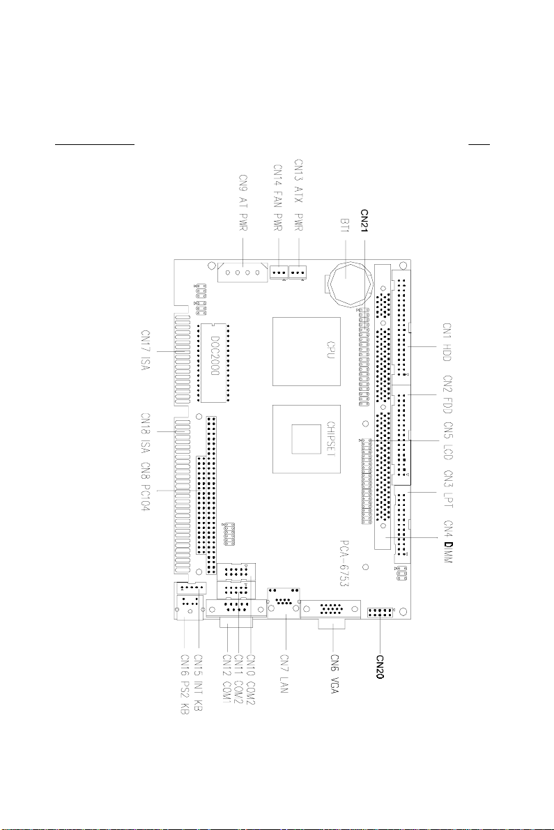
2.1 Board layout: Connector locations (component side)
Figure 2-1: Board Layout: Connector Locations(component side)
10 PCA-6753F User's Manual
Page 21

2.2 Locating jumpers
Figure 2-2: Locating Jumpers
Chapter 2 Connecting Peripherals 11
Page 22

2.3 Jumpers and connectors
Connectors on the board link it to external devices such as hard disk
drives, a keyboard or expansion bus connectors. In addition, the board
has a number of jumpers that allow you to configure your system to
suit your application.
The table below lists the function of each of the board jumpers and
connectors:
Table 2-1: Jumpers
Label
JP1 LCD Voltage select & wake-on-Lan
JP6 RS-232/RS-422/RS-485 select
JP8 DOC® 2000 Address select
JP9 CMOS clear & watchdog trigger output
12 PCA-6753F User's Manual
Page 23

The following table lists the connectors on the PCA-6753F.
Table 2-2: Connectors
Label Function
CN1 HDD connector
CN2 FDD connector
CN3 Printer port connector
CN4 DIMM connector
CN5 Flat panel display connector (18 bit)
CN6 VGA connector
CN7 LAN connector
CN8 PC/104 connector
CN9 AT (big 4P) power connector
CN10 COM2 connector (RS-232)
CN11 COM2 connector (RS-422/RS-485)
CN12 COM1 connector
CN13 ATX feature connector
CN15 Internal keyboard connector
CN16 PS/2 keyboard + PS/2 mouse connector
CN17 ISA Golden Finger connector
CN18 ISA Golden Finger connector
CN 20 USB connector
CN 21 Multiple connector
Chapter 2 Connecting Peripherals 13
Page 24

2.4 Setting jumpers
2.4.1 Introduction
You may configure your card to match the needs of your application
by setting jumpers. A jumper is the simplest kind of electrical switch.
It consists of two metal pins and a small metal clip (often protected by
a plastic cover) that slides over the pins to connect them. To "close" a
jumper, you connect the pins with the clip. To "open” a jumper you
remove the clip. Sometimes a jumper will have three pins, labeled 1,
2, and 3. In this case you would connect either pins 1 and 2 or 2 and 3.
3
2
1
Closed 2-3Open Closed
The jumper settings are schematically depicted in this manual as
follows:
1 2 3
Closed 2-3Open Closed
A pair of needle-nose pliers may be helpful when working with
jumpers.
If you have any doubts about the best hardware configuration for your
application, contact your local distributor or sales representative
before you make any changes.
Generally, you simply need a standard cable to make most connections.
14 PCA-6753F User's Manual
Page 25

2.4.2 Settings details
JP1: LCD Voltage select & Wake-up on LAN ATX PWR
Pin Function
1-3 LCD Panel VDD +3.3 V
3-5 LCD Panel VDD +5 V*
2-4 Wake-up on LAN ATX power standby
4-6 Normal condition*
2
2
2
2
1
LCD 3.3 V
External speaker connection
1
LCD 5V* WOL ATX Normal*
1
CN 21: 5-7 Result
Closed Internal speaker enabled
Open Internal speaker disabled
CN 21 Multiple connector location
1
Chapter 2 Connecting Peripherals 15
Page 26

JP6: RS-232/RS-422/RS-485 select
Pin Function
3-5,4-6,9-11,10-12,13-14 COM1/232*
19-20, use CN10 connector COM2/232*
21-22, use CN11 connector COM2/422
23-24, use CN11 connector COM2/485
2
12
24
COM1/232*
1
2
COM2/232*
1
2
COM2/422
1
2
COM2/485
1
JP8: DOC® 2000 Address select
®
COD
8PJ2-14-36-5
FFOFFOFFOFFO
FFFDD-000CDFFOnOFFO
FFF9D-0008DFFOnOnO
FFF5D-0004DnOFFOFFO
*FFF1D-000DnOFFOnO
FFFDC-000CCnOnOFFO
FFF9D-0008CnOnOnO
2311
12
24
2311
12
24
2311
12
24
2311
tcelessserdda0002
16 PCA-6753F User's Manual
Page 27

2
2
2
2
1
OFF
2
1
D000D1FFF*
1
DC000DDFFF
2
1
CC000CDFFF
1
D8000D9FFF
2
1
C8000D9FFF
1
D4000D5FFF
2.5 Watchdog timer action (JP9)
When the watchdog timer activates (CPU processing has come to a
halt), it can reset the system or generate an interrupt on IRQ11. This
can be set via JP9 as shown below:
2
1
IRQ11 Reset*
(2-4-6) CMOS clear
Pin Function
2-4 Normal*
4-6 Clear CMOS
2
1
2
1
Normal* Clear CMOS
2
1
Chapter 2 Connecting Peripherals 17
Page 28

The following sections tell how to make each connection. In most
cases, you will simply need to connect a standard cable. All of the
connector pin assignments are shown in Appendix A .
Warning! Always completely disconnect the power cord from
your chassis whenever you are working on it. Do not
make connections while the power is on. Sensitive
electronic components can be damaged by a
sudden rush of power. Only experienced electronics
personnel should open the PC chassis.
Caution! Always ground yourself to remove any static charge
before touching the CPU card. Modern electronic
devices are very sensitive to static electric charges.
Use a grounding wrist strap at all times. Place all
electronic components on a static-dissipative
surface or in a static-shielded bag when they are not
in the chassis.
2.6 Enhanced IDE connector (CN1)
You can attach two IDE (Integrated Device Electronics) drives to the
PCA-6753F internal controller. The PCA-6753F CPU card has an
EIDE connector, CN1.
Wire number 1 on the cable is red or blue, and the other wires are
gray. Connect one end to connector CN1 on the CPU card. Make sure
that the red (or blue) wire corresponds to pin 1 on the connector (on
the right side). See Chapter 1 for help in finding the connector.
Unlike floppy drives, IDE hard drives can connect in either position
on the cable. If you install two drives, you will need to set one as the
master and one as the slave. You do this by setting the jumpers on the
drives. If you use just one drive, you should set it as the master. See
the documentation that came with your drive for more information.
Connect the first hard drive to the other end of the cable. Wire 1 on
the cable should also connect to pin 1 on the hard drive connector,
which is labeled on the drive circuit board. Check the documentation
that came with the drive for more information.
Connect the second drive, as described above, on CN1.
18 PCA-6753F User's Manual
Page 29

2.7 FDD connector (CN2)
You can attach up to two floppy disk drives to the PCA-6753F's
onboard controller. You can use any combination of 5.25" (360 KB/
1.2 MB) and/or 3.5" (720 KB/1.44/2.88 MB) drives.
The card comes with a 34-pin daisy-chain drive connector cable. On
one end of the cable is a 34-pin flat-cable connector. On the other
end are two sets of floppy disk drive connectors. Each set consists of
a 34-pin flat-cable connector (usually used for 3.5" drives) and a
printed-circuit-board connector (usually used for 5.25" drives). You
can use only one connector in each set. The set on the end (after the
twist in the cable) connects to the A: floppy. The set in the middle
connects to the B: floppy.
2.8 Parallel port connector (CN3)
The parallel port is normally used to connect the CPU card to a
printer. The PCA-6753F includes an on-board parallel port, accessed
through a 26-pin flat-cable connector, CN3. The card comes with an
adapter cable which lets you use a traditional DB-25 connector. The
cable has a 26-pin connector on one end and a DB-25 connector on
the other, mounted on a retaining bracket. The bracket installs at the
end of an empty slot in your chassis, giving you access to the connector.
The parallel port is designated as LPT1, and can be disabled or
changed to LPT2 or LPT3 in the system BIOS setup.
To install the bracket, find an empty slot in your chassis. Unscrew the
plate that covers the end of the slot. Screw in the bracket in place of
the plate. Next, attach the flat-cable connector to CN3 on the CPU
card. Wire 1 of the cable is red or blue, and the other wires are gray.
Make sure that wire 1 corresponds to pin 1 of CN3. Pin 1 is on the
right side of CN3.
Chapter 2 Connecting Peripherals 19
Page 30

2.9 Flat panel display connector (CN5)
CN5 consists of a 44-pin, dual-in-line header.
The power supply (+12 V) for CN5 is dependant on the supply
connected to the board. Therefore make sure that CN9 is connected to
a +12 V power supply.
The PCA-6753F provides a bias control signal on CN5 which can be
used to control the LCD bias voltage. It is recommended that the LCD
bias voltage not be applied to the panel until the logic supply voltage
(+5 V or +3.3 V) and panel video signals are stable. Under normal
operation the control signal (ENAVEE) is active high. When the
PCA-6753F board's power is applied, the control signal is low until
just after the relevant flat panel signals are present.
2.10 VGA display connector (CN6)
The PCA-6753F provides a VGA controller for a high resolution
VGA interface. The PCA-6753F CN6 is a DB-15 connector for VGA
monitor input. Pin assignments for the CRT display are detailed in
Appendix A.
2.11 Ethernet connector (CN7)
The PCA-6753F is equipped with a high performance 32-bit PCI-bus
Fast Ethernet interface which is fully compliant with IEEE 802.3u
10/100Base-T specifications. It is supported by all major network
operating systems.
The medium type can be configured via the rset8139.EXE program
included on the utility disk. (See Chapter 5 for detailed information.)
2.12.1 Network boot
The network boot feature is built into the BIOS. It can be enabled or
disabled in the chipset setup of the CMOS configuration. Refer to
"BIOS Setting" in Chapter 4 for more information.
20 PCA-6753F User's Manual
Page 31

2.12 PC/104 connectors (CN8)
The PCA-6753F is equipped with a 16-bit ISA signal PC/104 connector for future expansion. See Appendix D for details.
2.13 AT power connector (CN9)
If you prefer not to acquire power through the PCA-6753F backplane
via the gold H-connectors, The big 4P power connector (CN9) also
provides power input connectors for +5 V, and +12 V.
2.14 Serial ports (CN12: COM1; CN10: COM2/RS-232; CN11: COM2/RS-422/485)
The PCA-6753F offers two serial ports: COM1 in RS-232 and COM2
(CN10: RS-232, CN11:RS-422/485). These ports let you connect to
serial devices (a mouse, printers, etc.) or a communication network.
You can select the address for each port (for example, 3F8H [COM1],
2F8H [COM2]) or disable each port. Use the BIOS Advanced Setup
program, which is covered in Chapter 4.
The card mounting bracket holds the serial port connector for the one
port. The parallel port and serial port adapter kit (supplied with the
card) holds the connector for the other port. This lets you connect and
disconnect cables after you install the card. The DB-9 connector on
the bottom of the bracket is the first RS-232 port, COM1. The DB-9
connector on the adapter kit is the second serial port, COM2.
Table 2-2: Serial port connections (COM1, COM2)
Connector Function
COM1 RS-232
COM2 RS-232/422/485
Chapter 2 Connecting Peripherals 21
Page 32

2.15.1 RS-232 connection (COM1: CN12)
Different devices implement the RS-232 standard in different ways. If
you are having problems with a serial device, be sure to check the pin
assignments for the connector.
2.15.2 RS-232/422/485 connection (COM2: CN10: RS-232; CN11: RS-422/485)
COM2 is an RS-232/422/485 serial port. The specific port type is
determined by jumper settings (JP6), as detailed in Chapter 1.
The IRQ and address range for both ports are fixed. However, if you
wish to disable the port or change these parameters later, you can do
this in the system BIOS setup. The table below shows the settings for
the PCA-6753F Series' board's ports:
Table 2-3: Serial port default settings
Port Address Interrupt Default
COM1 3F8, 3E8 IRQ4 3F8
COM2 2F8, 2E8 IRQ3 2F8
22 PCA-6753F User's Manual
Page 33

2.16 ATX Feature Connector (CN13)
When the PCA-6753F is used as a standalone card, the main power
connector (CN9) is used. If the PCA-6753F is used with a passive
backplane, the main power connector (CN9) should not be connected.
This is because the card will be powered from the backplane.
To ATX feature
connector (CN13)
P9 P8 P9
(P8) 6-pin in backplane
(P9) 6-pin in backplane
P8
20-pin female connector
Figure 2-4: ATX adaptor cable
The ATX adapter cable (provided) is used to connect the PCA-6753F
to the ATX power supply. The ATX adapter cable has different
connectors at both ends. On one end is the ATX 20-pin (female type)
which connects to the (male) ATX power supply source. The other
end has a 3-pin connector (female type) which connects to the ATX
feature connector (CN13) on the board itself. This end also has the
6-pin main power connector (P8) and a 6-pin connector (P9) which is
used when the board is mounted on a passive backplane.
ATX power supply source
2.17 Internal keyboard connector (CN15)
In addition to the PS/2 mouse/keyboard connector, an additional
external keyboard connector is provided.
For external keyboard pin assignments, see Appendix A.
Chapter 2 Connecting Peripherals 23
Page 34

2.18 Keyboard and PS/2 mouse connector (CN16)
The PCA-6753F board provides a keyboard connector. A 6-pin miniDIN connector (CN16) on the card mounting bracket supports singleboard computer applications. The card comes with an adapter to
convert from the 6-pin mini-DIN connector to a standard DIN
connector and to a PS/2 mouse connector.
2.19 ISA gold fingers (CN17, CN18)
The 16-bit ISA gold fingers are used for connecting the PCA-6753F
Series to an ISA passive backplane.
2.20 USB connector (CN20)
The PCA-6753F board provides two USB (Universal Serial Bus)
interfaces, which give complete plug and play and also hot
attach/detach for up to 127 external devices. The USB interfaces
comply with USB specification rev. 1.0 and are fuse protected.
The USB interfaces are accessed through a 10-pin flat-cable connector, CN20. The adapter cable has a 10-pin connector on one end and a
USB connector on the bracket.
The USB interfaces can be disabled in the system BIOS setup.
2.21 ATX power button (CN21, pins 2,4)
The PCA-6753F provides an ATX power input connector. When
connected with the ATX power switch, the ATX power switch
connector (CN21) enables power On/Off from the chassis.
24 PCA-6753F User's Manual
Page 35

2.22 Reset switch (CN21, pins 6,8)
If you install a reset switch, it should be a single pole switch rated at 10 mA, 5
V. Momentarily pressing the switch will activate a reset.
For reset switch pin assignments, please see Appendix A.
2.23 IR connector (CN21 pins 9,11,13,15,17)
This connector supports the optional wireless infrared transmitting and receiving module. This module mounts on the system case. You must configure the
setting through BIOS setup.
Chapter 2 Connecting Peripherals 25
Page 36

26 PCA-6753F User's Manual
Page 37

CHAPTER
3
Software Configuration
This chapter details the software configuration information. It shows you how to
configure the card to match your application requirements. Award system BIOS is
covered in Chapter 4.
Sections include:
• Connections for two standard LCDs
Page 38

3.1 Introduction
The PCA-6753F system BIOS and custom drivers are located in a
256 KB, 32-pin Flash ROM device, designated U15. A single
Flash chip holds the system BIOS and VGA BIOS.
3.2 Utility CD disk
The PCA-6753F is supplied with a software utility on CD-ROM.
This disk contains the necessary file for setting up the VGA
display. Directories and files on the disk are as follows:
AWDFLASH.EXE
CBROM.EXE
RSET8139.EXE
6753Vxxx.BIN
Figure 3-1: Contents of the PCA-6753 Series utility disk
AWDFLASH.EXE
This program allows you to update the BIOS Flash ROM.
6753sVxxx.BIN
This binary file contains the system BIOS.
CBROM.EXE
This program allows you to combine your own VGA BIOS with
system BIOS (6753V110.BIN).
RSET8139.EXE
This program enables you to view the current Ethernet configuration, reconfigure the Ethernet interface (medium type, etc.), and
execute useful diagnostic functions.
28 PCA-6753F User's Manual
Page 39

3.3 BIOS Program Setup
Note: Make sure that you do not run AWDFLASH.EXE
while your system is operating in EMM386 mode.
1. At the prompt, type AWDFLASH.EXE and press <Enter>. The
VGA configuration program will then display the following:
Figure 3-2: BIOS program setup screen
2. At the prompt, type in the BIN file which supports your
display. When you are sure that you have entered the file name
correctly press <Enter>. The screen will ask “Do you want to
save?” If you wish to continue press Y. If you change your
mind or have made a mistake press N.
3. If you decide to continue, the screen will issue a prompt which
will then ask “Are you sure to program (Y/N)?” If you wish to
continue, press Y. Press N to exit the program.
The new VGA configuration will then write to the ROM BIOS
chip. This configuration will remain the same until you run the
AWDFLASH.EXE program and change the settings.
Chapter 3 Software Configuration 29
Page 40

3.4 CBROM Implementation
The CBROM execute command gives users VGA BIOS setup options.
The first allows users to combine the VGA BIOS into the
original BIOS configuration. The second option allows users to
release the VGA BIOS from the original BIOS. To implement, use
the following commands:
1. CBROM 6753V110.BIN /VGA VGA.dat
This command combines the VGA BIOS into the original
BIOS. The file name that will be assigned to the VGA BIOS
later will be VGA.dat
2. CBROM 6753V110.BIN /VGA Release
This command releases the VGA BIOS from the original
BIOS.
30 PCA-6753F User's Manual
Page 41

3.5 Connections for two standard LCDs
3.5.1 Connections for Toshiba LTM10C042 (640 x 480 TFT color LCD)
Table 3-1: Connections for Toshiba LTM10C042
LTM10C042 PCA-6753 Series CN5
Pin Name Pin Name
1 GND 3 GND
2 CLK 35 SHFCLK
3 GND 4 GND
4 R0 27 PD12
5 R1 28 PD13
6 R2 29 PD14
7 GND 8 GND
8 R3 30 PD15
9 R4 31 PD16
10 R5 32 PD17
11 GND 33 GND
12 G0 19 PD6
13 G1 20 PD7
14 G2 21 PD8
15 GND 33 GND
16 G3 22 PD9
17 G4 23 PD10
18 G5 24 PD11
19 GND 34 GND
20 ENAB 37 M
21 GND 34 GND
22 B0 11 PD0
23 B1 12 PD1
24 B2 13 PD2
25 GND 39 GND
26 B3 14 PD3
27 B4 15 PD4
28 B5 16 PD5
29 GND 39 GND
30 VDD 5 +5 V
31 VDD 6 +5 V
Chapter 3 Software Configuration 31
Page 42

3.5.2 Connections for Toshiba LTM12C275A
(800 x 600 TFT color LCD)
Table 3-2: Connections for Toshiba LTM12C275A
LTM12C275A PCA-6753F CN5
Pin Name Pin Name
1 GND 3 GND
2 NCLK 35 SHFCLK
3NC - NC
4NC - NC
5 GND 4 GND
6 R0 27 PD12
7 R1 28 PD13
8 R2 29 PD14
9 R3 30 PD15
10 R4 31 PD16
11 R5 32 PD17
12 GND 8 GND
13 G0 19 PD6
14 G1 20 PD7
15 G2 21 PD8
16 G3 22 PD9
17 G4 23 PD10
18 G5 24 PD11
19 GND 33 GND
20 B0 11 PD0
21 B1 12 PD1
22 B2 13 PD2
23 B3 14 PD3
24 B4 15 PD4
25 B5 16 PD5
26 ENAB 37 M/DE
27 GND 34 GND
28 VCC 5 +5 V
29 VCC 6 +5 V
30 GND 39 GND
32 PCA-6753F User's Manual
Page 43

3.6 Ethernet interface configuration
The PCA-6753F on-board Ethernet interface supports all major
network operating systems. To configure the medium type, to
view the current configuration, or to run diagnostics, do the
following:
1. Power the PCA-6753F on. Make sure that the RSET8139.EXE
file is located in the working drive.
2. At the prompt, type RSET8139.EXE and press <Enter>. The
Ethernet configuration program will then be displayed.
3. This simple screen shows all the available options for the
Ethernet interface. Just highlight the option you wish to change
by using the Up and Down keys. To change a selected item,
press <Enter>, and a screen will appear with the available
options. Highlight your option and press <Enter>. Each
highlighted option has a helpful message guide displayed at the
bottom of the screen for additional information.
4. After you have made your selections and are sure this is the
configuration you want, press ESC. A prompt will appear
asking if you want to save the configuration. Press Y if you
want to save.
The Ethernet Setup Menu also offers three very useful diagnostic
functions. These are:
1. Run EEPROM test
2. Run Diagnostics on Board
3. Run Diagnostics on Network
Each option has its own display screen that shows the format and
result of any diagnostic tests undertaken.
Chapter 3 Software Configuration 33
Page 44

34 PCA-6753F User's Manual
Page 45

CHAPTER
4
Award BIOS Setup
This chapter describes how to set BIOS
configuration data.
Page 46

4.1 System test and initialization
These routines test and initialize board hardware. If the routines
encounter an error during the tests, you will either hear a few short
beeps or see an error message on the screen. There are two kinds
of errors: fatal and non-fatal. The system can usually continue the
boot up sequence with non-fatal errors. Non-fatal error messages
usually appear on the screen along with the following instructions:
press <F1> to RESUME
Write down the message and press the F1 key to continue the
bootup sequence.
4.1.1 System configuration verification
These routines check the current system configuration against the
values stored in the board’s CMOS memory. If they do not match,
the program outputs an error message. You will then need to run
the BIOS setup program to set the configuration information in
memory.
There are three situations in which you will need to change the
CMOS settings:
1. You are starting your system for the first time
2. You have changed the hardware attached to your system
3. The CMOS memory has lost power and the configuration
information has been erased.
The PCA-6753F CMOS memory has an integral lithium battery
backup. The battery backup should last ten years in normal
service, but when it finally runs down, you will need to replace the
complete unit.
36 PCA-6753F User's Manual
Page 47

4.2 Award BIOS setup
Award’s BIOS ROM has a built-in Setup program that allows
users to modify the basic system configuration. This type of
information is stored in battery-backed CMOS RAM so that it
retains the Setup information when the power is turned off.
4.2.1 Entering setup
Power on the computer and press <Del> immediately. This will
allow you to enter Setup.
Figure 4-1: BIOS setup program initial screen
Chapter 4 Award BIOS Setup 37
Page 48

4.2.2 Standard CMOS setup
When you choose the STANDARD CMOS SETUP option from
the INITIAL SETUP SCREEN menu, the screen shown below is
displayed. This standard Setup Menu allows users to configure
system components such as date, time, hard disk drive, floppy
drive and display. Once a field is highlighted, on-line help
information is displayed in the left bottom of the Menu screen.
Figure 4-2: CMOS setup screen
38 PCA-6753F User's Manual
Page 49

4.2.3 BIOS features setup
By choosing the BIOS FEATURES SETUP option from the
INITIAL SETUP SCREEN menu, the screen below is displayed.
This sample screen contains the manufacturer’s default values for
the PCA-6753F.
Figure 4-3: BIOS features setup
Chapter 4 Award BIOS Setup 39
Page 50

4.2.4 Chipset features setup
By choosing the CHIPSET FEATURES SETUP option from the
INITIAL SETUP SCREEN menu, the screen below is displayed.
This sample screen contains the manufacturer’s default values for
the PCA-6753F.
Figure 4-4: Chipset features setup
40 PCA-6753F User's Manual
Page 51

4.2.5 Power management setup
By choosing the POWER MANAGEMENT SETUP option from
the INITIAL SETUP SCREEN menu, the screen below is displayed. This sample screen contains the manufacturer’s default
values for the PCA-6753F.
Figure 4-5: Power management setup
Chapter 4 Award BIOS Setup 41
Page 52

4.2.6 PnP/PCI configuration
By choosing the PnP/PCI CONFIGURATION option from the
Initial Setup Screen menu, the screen below is displayed. This
sample screen contains the manufacturer’s default values for the
PCA-6753F.
Figure 4-6: PnP/PCI configuration
42 PCA-6753F User's Manual
Page 53

4.2.7 Integrated peripherals
By choosing the INTEGRATED PERIPHERALS option from the
INITIAL SETUP SCREEN menu, the screen below is displayed.
This sample screen contains the manufacturer’s default values for
the PCA-6753F. The PANEL TYPE by default supports a 18-bit
640 x 480 TFT LCD panel display.
Figure 4-7: Integrated peripherals
Chapter 4 Award BIOS Setup 43
Page 54

4.2.8 Change password
To change the password, choose the PASSWORD SETTING
option form the Setup main menu and press <Enter>.
1. If the CMOS is bad or this option has never been used, a
default password is stored in the ROM. The screen will display
the following messages:
Enter Password:
Press <Enter>.
2. If the CMOS is good or this option has been used to change the
default password, the user is asked for the password stored in
the CMOS. The screen will display the following message:
Confirm Password:
Enter the current password and press <Enter>.
3. After pressing <Enter> (ROM password) or the current
password (user-defined), you can change the password stored
in the CMOS. The password can be at most eight (8) characters
long.
Remember - to enable this feature, you must first select either
Setup or System in the BIOS FEATURES SETUP.
44 PCA-6753F User's Manual
Page 55

4.2.9 Save & exit setup
If you select this option and press <Enter>, the values entered in
the setup utilities will be recorded in the chipset’s CMOS memory.
The microprocessor will check this every time you turn your
system on and compare this to what it finds as it checks the
system. This record is required for the system to operate.
4.2.10 Exit without saving
Selecting this option and pressing <Enter> lets you exit the Setup
program without recording any new values or changing old ones.
Chapter 4 Award BIOS Setup 45
Page 56

46 PCA-6753F User's Manual
Page 57

CHAPTER
SVGA Setup
• Introduction
• Installation of SVGA driver for
Windows 3.1/9x/NT
5
Page 58

5.1 Introduction
The PCA-6753F has an on-board LCD/VGA interface. The
specifications and features are described as follows:
5.1.1 Chipset
The PCM-6753F uses a NS CX5530 chipset for its SVGA
controller. It supports many popular 18-bit LCD displays and
conventional analog CRT monitors. The VGA BIOS supports
LCD. In addition, it also supports interlaced and non-interlaced
analog monitors (color and monochrome VGA) in high-resolution
modes while maintaining complete IBM VGA compatibility.
Digital monitors (i.e. MDA, CGA, and EGA) are NOT supported.
Multiple frequency (multisync) monitors are handled as if they
were analog monitors.
5.1.2 Display memory
With 1.5 ~ 4 MB shared memory, the VGA controller can drive
CRT displays or color panel displays with resolutions up to 1280 x
1024 at 256 colors. The display memory can be expanded to 4 MB
in BIOS for 64K color resolution of 1024 x 768.
48 PCA-6753F User's Manual
Page 59

5.2 Installation of SVGA driver
Complete the following steps to install the SVGA driver. Follow
the procedures in the flow chart that apply to the operating system
that you are using within your PCM-6753F.
Important: The following windows illustrations are examples
only. You must follow the flow chart instructions
and pay attention to the instructions which then
appear on your screen.
Note 1: The CD-ROM drive is designated as "D:"
throughout this chapter.
Note 2: <Enter> means pressing the “Enter” key on the
keyboard.
Note 3: When you are using a CRT display, please make
sure that your flat panel resolution settings (in the
BIOS setup) are the same as your VGA resolution settings (in Windows). Otherwise your
display may behave strangely.
Chapter 5 SVGA Setup 49
Page 60

5.2.1 Installation for Windows 3.1
1. In the Windows 3.1 Main screen, click on the "Windows
Setup" icon.
2. In the "Windows Setup" window, choose "Options", then select
"Change System Settings".
50 PCA-6753F User's Manual
Page 61

3. In the "Change System Settings" window, select the "Display"
item. In the dropdown selection, select "Other display {Requires disk from OEM}" .
4. Type in the correct path like the window below, where drive
"D" is the CD ROM drive. For example,
D:\slotpc\6753\VGA\WIN31
Chapter 5 SVGA Setup 51
Page 62

5. Select the display type and preferred resolution, then click
"OK".
6. Choose "Restart Windows".
52 PCA-6753F User's Manual
Page 63

5.2.2 Installation for Cyrix MediaGX Certified drivers for Windows 95/98
1. Insert the disk into the CD-ROM drive.
Select "Start" then "Run".
Type the correct path for the driver (like the example below)
"D:\slotpc\6753\VGA\Win9xc_40"
Click "OK"
Chapter 5 SVGA Setup 53
Page 64

2. Click "Finish" to continue.
3. Click "Next" to proceed to the next step. Click "Yes" after you read
the license agreement.
54 PCA-6753F User's Manual
Page 65

4. Follow the instructions which appear on the screen.
5. Insert the Win95/98 CD-ROM into the CD-ROM drive. Type the
correct path for the Win9x source file.
Chapter 5 SVGA Setup 55
Page 66

6. Choose "Yes" then click "Finish" to restart the computer.
56 PCA-6753F User's Manual
Page 67

5.2.3 Installation for Windows NT
1. a. Select "Start", "Settings" then "Control Panel" to get to the screen
below.
b. Double click on the "Display" icon.
2. a. Choose the "Settings" selection.
b. Click the "Display Type" button.
Chapter 5 SVGA Setup 57
Page 68

3. Press the "Change..." button.
4. Click on the "Have Disk..." button
58 PCA-6753F User's Manual
Page 69

5. a. Insert the disk into the CD-ROM drive.
b. Type "D:\slotpc\6753\VGA\WINNT" in the blank.
c. Press "OK".
6. a. Select the highlighted item.
b. Press "OK".
7. Press "Yes" to proceed.
Chapter 5 SVGA Setup 59
Page 70

8. Press "OK" to reboot.
9. a. Repeat Step 1 in this manual, select the "Settings" label.
b. Adjust the resolution and color.
c. Click "Test" to see the results.
d. Click "OK" to save the settings.
60 PCA-6753F User's Manual
Page 71

5.3 Further information
For further information about the PCI/SVGA installation in your
PCA-6753F, including driver updates, troubleshooting guides and FAQ
lists, visit the following web resources:
Cyrix web site: www.national.com
Advantech web sites: www.advantech.com
www.advantech.com.tw
Chapter 5 SVGA Setup 61
Page 72

62 PCA-6753F User's Manual
Page 73

CHAPTER
6
PCI Bus Ethernet
Interface
This chapter provides information on
Ethernet configuration.
• Introduction
• Installation of Ethernet driver for
Windows 95/98/NT
• Further information
Page 74

6.1 Introduction
The PCA-6753F is equipped with a high performance 32-bit
Ethernet chipset which is fully compliant with IEEE 802.3 100
Mbps CSMA/CD standards. It is supported by major network
operating systems. It is also both 100Base-T and 10Base-T
compatible. The medium type can be configured via the
RSET8139.exe program included on the utility disk.
The Ethernet port provides a standard RJ-45 jack on board. The
network boot feature can be utilized by incorporating the boot
ROM image files for the appropriate network operating system.
The boot ROM BIOS files are combined with system BIOS, which
can be enabled/disabled in the BIOS setup.
6.2 Installation of Ethernet driver
Before installing the Ethernet driver, note the procedures below.
You must know which operating system you are using in your
PCA-6753F, and then refer to the corresponding installation flow
chart. Then just follow the steps described in the flow chart. You
will quickly and successfully complete the installation, even if you
are not familiar with instructions for MS-DOS or Windows.
Note: The windows illustrations in this chapter are
examples only. You must follow the flow chart
instructions and pay attention to the instructions
which then appear on your screen.
6.2.1 Installation for MS-DOS and Windows 3.1
If you want to set up your Ethernet connection under the MS-DOS
or Windows 3.1 environment, you should first check your server
system model. For example, MS-NT, IBM-LAN server, and so on.
Then choose the correct driver to install in your panel PC.
The installation procedures for various servers can be found on
CD-ROM; the correct path being "D:\6753\Ethernet.100\wfw311".
64 PCA-6753F User's Manual
Page 75

6.2.2 Installation for Windows 95/98
1. a. Select "Start", "Settings", "Control Panel".
b. Double click "Network"
2. Click "Add" and prepare to install network functions.
Chapter 6 PCI Bus Ethernet Interface 65
Page 76

3. Select the "Adaptor" item to add the Ethernet card.
4. Click "Have Disk" to install the driver.
5. a. Insert the CD_ROM into the D:\drive.
b. Type "D:\slotpc\Ethernet\Win95".
c. Click "OK".
66 PCA-6753F User's Manual
Page 77

6. a. Choose the "Realtek" item.
b. Click "OK"
7. a. Make sure the configurations of the relative items are set
correctly.
b. Click "OK" to reboot.
Note: The correct path for Windows 98 is:
"D:\slotpc\Ethernet\Win98"
Chapter 6 PCI Bus Ethernet Interface 67
Page 78

6.2.3 Installation for Windows NT
1. a. Select "Start", "Settings", "Control Panel".
b. Double click "Network".
2. a. Choose the "Adaptors" label.
b. Click the "Add" button.
68 PCA-6753F User's Manual
Page 79

3. Press "Have Disk".
4. a. Type "D".
b. Press "OK".
5. a. Insert the CD-ROM into the D:\drive
b. Type "D:\slotpc\Ethernet\Winnt\"
c. Click "OK".
Chapter 6 PCI Bus Ethernet Interface 69
Page 80

6. a. Choose the "Realtek" item.
b. Click "OK".
7. a. Make sure the configurations for the relative items are set
correctly.
b. Click "OK" to reboot.
70 PCA-6753F User's Manual
Page 81

6.3 Further information
Realtek website: www.realtek.com
Advantech websites: www.advantech.com
www.advantech.com.tw
Chapter 6 PCI Bus Ethernet Interface 71
Page 82

72 PCA-6753F User's Manual
Page 83

APPENDIX
A
Pin Assignments
This appendix contains information of a
detailed or specialized nature. It includes:
• IDE hard drive connector
• Floppy drive connector
• Parallel port connector
• CRT display connector
• Flat panel display connector
• Ethernet 10/100Base-T connector
• AT power connector
• COM2 RS-232/422/485 serial port
connector
• COM1 RS-232 serial port
• Auxilary power connector
• CPU fan power connector
• Keyboard and mouse connector
Page 84

IDE hard drive connector (CN1)
Table C-1: IDE hard drive connector
Pin Signal Pin Signal
1 IDE RESET* 2 GND
3 DATA 7 4 DATA 8
5 DATA 6 6 DATA 9
7 DATA 5 8 DATA 10
9 DATA 4 10 DATA 11
11 DATA 3 12 DATA 12
13 DATA 2 14 DATA 13
15 DATA 1 16 DATA 14
17 DATA 0 18 DATA 15
19 SIGNAL GND 2 0 N/C
21 DRQ* 22 GND
23 IO WRITE* 24 GND
25 IO READ* 26 GND
27 IO CHANNEL READY 28 N/C
29 ACK 30 GND
31 IRQ14 (IDE IRQ) 32 IOCS16*
33 ADDR 1 34 N/C
35 ADDR 0 36 ADDR 2
37 HARD DISK 38 HARD DISK
SELECT 0 SELECT 1
39 IDE ACTIVE* 40 GND
* low active
74 PCA-6753F User's Manual
Page 85

Floppy drive connector (CN2)
33
31 1
32
Table C-2: Floppy drive connector
3
434
2
Pin Signal Pin Signal
1 GND 2 DENSITY SELECT*
3 GND 4 N/C
5 GND 6 N/C
7 GND 8 INDEX*
9 GND 10 MOTOR 0*
11 GND 12 DRIVE SELECT 1*
13 GND 14 DRIVE SELECT 0*
15 GND 16 MOTOR 1*
17 GND 18 DIRECTION*
19 GND 20 STEP*
21 GND 22 WRITE DATA*
23 GND 24 WRITE GATE*
25 GND 26 TRACK 0*
27 GND 28 WRITE PROTECT*
29 GND 30 READ DATA*
31 GND 32 HEAD SELECT*
33 GND 34 DISK CHANGE*
* low active
Appendix A Pin Assignments 75
Page 86

Parallel port connector (CN3)
25 3
23 1
24
Table C-3: Parallel port connector
Pin Signal
1 STROBE*
2 AUTOFD*
3D0
4 ERROR*
5D1
6 INIT*
7D2
8 SLCTINI*
9D3
10 GND
11 D4
12 GND
13 D5
14 GND
15 D6
16 GND
17 D7
18 GND
19 ACK*
20 GND
21 BUSY
22 GND
23 PE
24 GND
25 SLCT
26 GND
* low active
426
2
76 PCA-6753F User's Manual
Page 87

Flat panel display connector (CN5)
Table C-4: Flat panel display connector
Pin Function Pin Function
1 +12 V 2 +12 V
3 GND 4 GND
5 Vcc_LCD 6 Vcc_LCD
7 N/C 8 GND
9 N/C 10 N/C
11 PD0 12 PD1
13 PD2 14 PD3
15 PD4 16 PD5
17 N/C 18 N/C
19 PD6 20 PD7
21 PD8 22 PD9
23 PD10 24 PD11
25 N/C 26 N/C
27 PD12 28 PD13
29 PD14 30 PD15
31 PD16 32 PD17
33 GND 34 GND
35 SHFCLK 36 FLM
37 DE (M) 38 LP
39 GND 40 ENABKL
41 N/C 42 N/C
43 VSAFE (ENAVDD) 44 Vcc_LCD
Appendix A Pin Assignments 77
Page 88

CRT Display Connector (CN 6)
5
6
10
15
Table C-5: CRT display connector
Pin Signal Pin Signal
1 RED 9 N/C
2 GREEN 10 GND
3 BLUE 11 N/C
4 N/C 12 N/C
5 GND 13 H-SYNC
6 GND 14 V-SYNC
7 GND 15 N/C
8 GND
1
6
11
78 PCA-6753F User's Manual
Page 89

AT power connector (CN9)
1
2
3
4
Table C-7: AT power connector
Pin Signal
1 +12 V
2 GND
3 GND
4 +5 V
COM2 RS-232 connector (CN10)
1
3
5
7
9
Table C-8: COM2 RS-232 connector
2
4
6
8
10
Pin RS-232 port Pin RS-232 port
1 DCD 6 CTS
2 DSR 7 DTR
3 RxD 8 RI
4 RTS 9 GND
5 TxD 10 N/C
Appendix A Pin Assignments 79
Page 90

COM2 RS-422/485 connector (CN11)
1
3
5
7
9
Table C-9: COM2 RS-232/422/485 connector
2
4
6
8
10
Pin RS-422 port RS-485 port
1 TXD- DATA2 N/C N/C
3 TXD+ DATA+
4 N/C N/C
5 RXD+ N/C
6 N/C N/C
7 RXD- N/C
8 N/C N/C
9 GND GND
10 N/C N/C
COM1 RS-232 connector (CN12)
324
15
6
78
9
Table C-10: COM1 RS-232 connector
Pin Signal
1 DCD
2 RXD
3 TXD
4DTR
5GND
6 DSR
7 RTS
8 CTS
9RI
80 PCA-6753F User's Manual
Page 91

ATX power connector (CN13)
1
2
3
Table C-11: ATX power connector
Pin Signal
1 5 V SB
2 N/C
3 PS_ON
CPU fan power connector (CN14)
1
Table C-12: CPU fan power connector
Pin Signal
1 +5 V
2 GND
3 +12 V
2
3
Appendix A Pin Assignments 81
Page 92

Internal keyboard connector (CN15)
5
4
3
2
1
Table C-13: External keyboard connector
Pin Signal
1 CLK
2 DATA
3NC
4GND
5+ 5 V
Keyboard and mouse connnector (CN16)
4
Table C-14: Keyboard and mouse connector
Pin Signal
1 KB DATA
2 MS DATA
3 GND
4V
CC
5 KB CLOCK
6 MS CLOCK
82 PCA-6753F User's Manual
6
5
3
12
Page 93

CN21- HDD LED connector (pins 20,22)
CN21: HDD LED connector
Pin Signal
20 IDE LED +
22 IDE LED -
CN21- System reset switch conn (pins 6,8)
CN21: System reset switch connector
Pin Signal
6 MR_RESET
8 GND
Appendix A Pin Assignments 83
Page 94

CN21- ATX power button (pins 2,4)
CN21: ATX power button
Pin Signal
2 Power ON
4 GND
CN21- IR connector (pins 9,11,13,15,17)
CN21: IR connector
Pin Signal
9 +5 V
11 N/C
13 IR_RX
15 GND
17 IR_TX
84 PCA-6753F User's Manual
Page 95

CN21- External speaker (pins 1,3,5,7)
CN21: External speaker connector
Pin Signal
1+ 5 V
3 N/C
5 Internal speaker input
7 External speaker signal
Appendix A Pin Assignments 85
Page 96

86 PCA-6753F User's Manual
Page 97

APPENDIX
B
System Assignments
• System I/O ports
• DMA channel assignments
• Interrupt assignments
• 1st MB memory map
Page 98

B.1 System I/O ports
Table B-1: System I/O ports
Addr. range
(Hex) Device
000-01F DMA controller
020-021 Interrupt controller 1, master
022-023 Chipset address
040-05F 8254 timer
060-06F 8042 (keyboard controller)
070-07F Real-time clock, non-maskable interrupt (NMI) mask
080-09F DMA page register,
0A0-0BF Interrupt controller 2
0C0-0DF DMA controller
0F0 Clear math co-processor
0F1 Reset math co-processor
0F8-0FF Math co-processor
170- 178 2nd fixed disk for CompactFlash
1F0-1F8 1st fixed disk
200-207 Game I/O
278-27F Reserved
2F8-2FF Serial port 2
300-31F Ethernet**
360-36F Reserved
378-37F Parallel printer port 1 (LPT2)
380-38F SDLC, bisynchronous 2
3A0-3AF Bisynchronous 1
3B0-3BF Monochrome display and printer adapter (LPT1)
3C0-3CF Reserved
3D0-3DF Color/graphics monitor adapter
3F0-3F7 Diskette controller
3F8-3FF Serial port 1
443 Watchdog timer
** default setting
88 PCA-6753F User's Manual
Page 99

B.2 DMA channel assignments
Table B-2: DMA channel assignments
Channel Function
0 Available
1 Available
2 Floppy disk (8-bit transfer)
3 Parallel**
4 Cascade for DMA controller 1
5 Available
6 Available
7 Available
** Parallel port DMA default setting: DMA 3
Parallel port DMA select: DMA 1.3
Appendix B System Assignments 89
Page 100

B.3 Interrupt assignments
Table B-3: Interrupt assignments
Interrupt# Interrupt source
NMI Parity error detected
IRQ 0 Interval timer
IRQ 1 Keyboard
IRQ 2 Interrupt from controller 2 (cascade)
IRQ 8 Real-time clock
IRQ 9 Reserve
IRQ 10 Available
IRQ 11 Reserved for watchdog timer
IRQ 12 PS/2 mouse
IRQ 13 INT from co-processor
IRQ 14 Preliminary IDE
IRQ 15 Secondary IDE for CompactFlash
IRQ 3 Serial communication port 2
IRQ 4 Serial communication port 1
IRQ 5 Available
IRQ 6 Diskette controller (FDC)
IRQ 7 Parallel port 1 (print port)
USB and Ethernet IRQ is automatically set by the system
90 PCA-6753F User's Manual
 Loading...