


PCA-6751 Series
Half-size all-in-one Pentium® CPU
card with MMX CPU, VGA/LCD and
Fast Ethernet interface
User’s Manual

Copyright notice
This document is copyrighted, 2000, by Advantech Co., Ltd. All
rights are reserved. The original manufacturer reserves the right to
make improvements to the products described in this manual at any
time without notice.
No part of this manual may be reproduced, copied, translated or
transmitted in any form or by any means without the prior written
permission of the original manufacturer. Information provided in this
manual is intended to be accurate and reliable. However, the original
manufacturer assumes no responsibility for its use, nor for any
infringements upon the rights of third parties which may result from
its use.
Acknowledgements
Award is a trademark of Award Software International, Inc.
IBM, PC/AT, PS/2 and VGA are trademarks of International Business
Machines Corporation.
Intel and Pentium are trademarks of Intel Corporation.
Microsoft Windows® is a registered trademark of Microsoft Corp.
UMC is a trademark of United Microelectronics Corporation.
All other product names or trademarks are properties of their
respective owners.
For more information on this and other Advantech products please
visit our websites at: http://www.advantech.com
http://www.advantech.com/epc
For technical support and service for please visit our support website
at: http://www.advantech.com/support
This manual is for the PCA-6751, PCA-6751V, PCA-6751L Rev. A1
and above.
Part No. 2006675112
3rd Edition Published in Taiwan April 2000

Packing list
Before installing your board, ensure that the following materials have
been received:
• 1 PCA-6751 Series all-in-one single board computer
• 2 utility disk with Ethernet utility programs
• 430 TX chipset driver for Windows 95
• 3 utility disks with SVGA utility programs and drivers for Windows
3.1/95/98/NT
• 1 hard disk drive (IDE) interface cable (40 pin)
• 1 floppy disk drive interface cable (34 pin)
• 1 parallel port adapter (26 pin) and COM2 adapter (9 pin) kit
• 1 6-pin mini-DIN keyboard and PS/2 mouse adapter
• 1ATX power adapter cable
• 1 warranty certificate
If any of these items are missing or damaged, contact your distributor
or sales representative immediately.
Optional devices
• IrdA adapter (part#: 968900042)
• 1 USB cable (part #1700100170)

Contents
Chapter 1 Hardware Configuration ...................................... 1
1.1 Introduction .................................................................................2
Embedded Pentium® MMX CPU .................................................2
Guaranteed long product supply time ..........................................2
1.2 Specifications ...............................................................................3
Standard SBC functions................................................................ 3
VGA function................................................................................3
Ethernet controller functions (PCA-6751 only) ...........................4
Solid state disk .............................................................................. 4
Mechanic and environmental specifications ................................ 4
PCA-6751 Series' models comparison table ................................4
1.3 Board layout: Dimensions ..........................................................5
1.4 Safety precautions .......................................................................6
1.5 Jumper settings............................................................................7
1.5.1 Introduction..........................................................................7
1.5.2 Locating jumpers ................................................................. 8
1.5.3 COM2 settings for RS-232/422/485 (JP1) ..........................9
1.5.4 LCD panel select (JP2) ........................................................9
1.5.5 CMOS backup select (JP3) ................................................ 11
1.5.6 Watchdog timer configuration (JP4) .................................12
1.6 Installing system memory (SODIMMs) .................................. 13
1.6.1 Installing SODIMMs ......................................................... 13
Chapter 2 Connecting Peripherals..................................... 15
2.1 Board layout: Connector locations (component side) ...........16
2.2 Board layout: Connector locations (solder side) ...................17
2.3 FDD connector (CN1) ...............................................................19
2.4 Parallel port connector (CN2) ................................................. 20
2.5 Keyboard lock, LED connector (CN3)....................................20
2.6 USB connector (CN4)................................................................20
2.7 24-bit LCD display connector (CN5) ...................................... 21
2.8 36-bit LCD display connector (CN6) ...................................... 21
2.9 LCD inverter connector (CN7)................................................ 21
2.10 IR connector (CN8)................................................................... 21

2.11 External speaker connector (CN9).......................................... 21
2.12 VGA display connector (CN11) ...............................................22
2.13 PC/104 connectors (CN12) .......................................................22
2.14 Ethernet connector (CN13) (PCA-6751 only) ........................2 2
2.14.1 RJ-45A connector (CN13)............................................... 22
2.14.2 Network boot ................................................................... 22
2.15 Serial ports (CN16: COM1; CN15: COM2/RS-232;
CN14: COM2/RS-422/485)....................................................... 2 3
2.15.1 RS-232 connection (COM1: CN16)................................ 2 3
2.15.2 RS-232/422/485 connection (COM2: CN15: RS-232;
CN14: RS-422/485) ...........................................................24
2.16 External keyboard connector (CN17)..................................... 2 4
2.17 ATX power connector (CN18) .................................................2 4
2.18 AT power connector (CN20) .................................................... 25
2.19 Keyboard and PS/2 mouse connector (CN21)........................ 25
2.20 ISA gold fingers (CN22, CN23) ............................................... 25
2.21 CompactFlash™ disk (CN24) ..................................................25
2.22 Front panel connector (CN25, CN26, CN27) .........................26
2.22.1 Hard disk drive LED (CN25) .......................................... 2 6
2.22.2 Reset switch (CN26) ........................................................ 26
2.22.3 ATX power button (CN27).............................................. 2 6
2.23 Enhanced IDE connector (CN28) ............................................ 27
2.24 ATX Feature Connector (CN27) .............................................28
Chapter 3 Award BIOS Setup ............................................. 29
3.1 Introduction ...............................................................................30
3.2 Entering setup............................................................................ 30
3.3 Standard CMOS setup.............................................................. 31
3.4 BIOS features setup ..................................................................32
3.5 Chipset features setup............................................................... 36
3.6 Power management setup......................................................... 37
3.7 PnP PCI configuration setup ................................................... 38
3.8 Load BIOS defaults...................................................................38
3.9 Load setup defaults ...................................................................38
3.10 Integrated peripherals ..............................................................39
3.11 Password setting ........................................................................ 39
3.12 IDE HDD auto detection ..........................................................40
3.13 Save & exit setup .......................................................................40
3.14 Exit without saving....................................................................40

Chapter 4 PCI SVGA Setup ................................................. 41
4.1 Introduction ...............................................................................42
4.1.1 Chipset ...............................................................................42
4.1.2 Display memory.................................................................42
4.1.3 Display types...................................................................... 42
4.2 Installation of SVGA driver..................................................... 43
4.2.1 Installation for Windows 3.1 .............................................44
4.2.2 Installation for Windows 95 ..............................................46
4.2.3 Installation for Windows NT ............................................. 49
4.3 Further information.................................................................. 52
Chapter 5 PCI Bus Ethernet Interface With Intel
®
SB82558/SB82559 (PCA-6751 only).................. 53
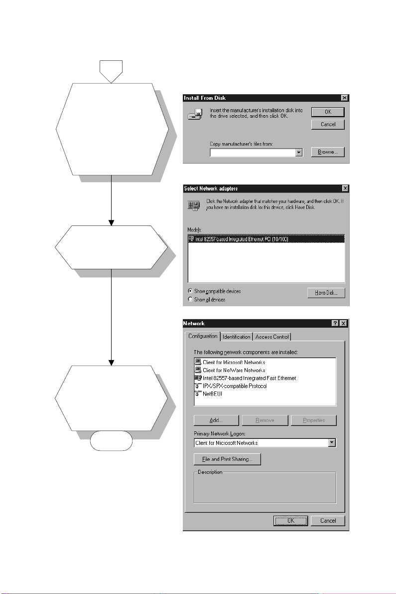
5.1 Introduction ...............................................................................54
5.2 Installation of Ethernet driver.................................................54
5.2.1 Installation for MS-DOS and Windows 3.1 ......................54
5.2.2 Installation for Windows 95 ..............................................55
5.2.3 Installation for Windows NT ............................................. 57
5.3 Further information.................................................................. 59
Chapter 6 PCI Bus Ethernet Interface With RTL-8139
(PCA-6751 only).................................................. 61
6.1 Introduction ...............................................................................62
6.2 Installation of Ethernet driver.................................................62
6.2.1 Installation for MS-DOS and Windows 3.1 ......................62
6.2.2 Installation for Windows 95/98 .........................................6 3
6.2.3 Installation for Windows NT ............................................. 65
6.3 Further information.................................................................. 67

Appendix A Programming the Watchdog Timer .............. 69
A.1 Programming the watchdog timer ..........................................70
Appendix B Installing PC/104 Modules ............................. 73
B.1 Installing PC/104 modules........................................................ 74
Appendix C Pin Assignments............................................. 77
C.1 Floppy drive connector (CN1) .................................................78
C.2 Parallel port connector (CN2) ................................................. 79
C.3 Keyboard lock, LED connector (CN3).................................... 8 0
C.4 USB1/USB2 connector (CN4)................................................... 80
C.5 24-bit LCD display connector (CN5) ...................................... 81
C.6 36-bit LCD display connector (CN6) ...................................... 82
C.7 LCD inverter connector (CN7)................................................ 83
C.8 IR connector (CN8)................................................................... 83
C.9 External speaker connector (CN9).......................................... 84
C.10 VGA connector (CN11) ............................................................ 8 4
C.11 PC/104 connector (CN12)......................................................... 85
C.12 Ethernet connector (CN13) ......................................................85
C.13 COM2 RS-422/485 connector (CN14)..................................... 8 6
C.14 COM2 RS-232 connector (CN15)............................................87
C.15 COM1 RS-232 connector (CN16)............................................88
C.16 External keyboard connector (CN17)..................................... 8 8
C.17 ATX power connector (CN18) .................................................8 9
C.18 AT power connector (CN20) .................................................... 89
C.19 Keyboard and PS/2 mouse connector (CN21)........................ 90
C.20 CompactFlash™ card connector (CN24) ...............................91
C.21 HDD LED connector (CN25) ...................................................92
C.22 System reset switch connector (CN26).................................... 92
C.23 ATX power button (CN27).......................................................92
C.24 Enhanced IDE connector (CN28) ............................................ 93
Appendix D System Assignments ..................................... 95
D.1 System I/O ports........................................................................ 96
D.2 DMA channel assignments .......................................................97
D.3 Interrupt assignments............................................................... 98
D.4 1st MB memory map................................................................. 99
Appendix E LCD Services................................................. 101
E.1 LCD services ............................................................................102

Tables
Table 1-1: Jumpers .......................................................................................... 8
Table 1-2: COM2 settings for RS-232/422/485 (JP1) ...................................... 9
Table 1-3: LCD panel select (JP2) ..................................................................10
Table 1-4: RTC power and CMOS clear (JP3) ................................................ 11
Table 1-5: Watchdog timer system reset select (JP4) ................................... 12
Table 2-1: Connectors ....................................................................................18
Table 2-2: Serial port connections (COM1, COM2) ........................................ 23
Table 2-3: Serial port default settings ............................................................24
Table B-1: PCA-6751 Series PC/104 connectors (CN12) ...............................76
Table C-1: Floppy drive connector (CN1) ....................................................... 78
Table C-2: Parallel port connector (CN2) .......................................................79
Table C-3: Keyboard lock, LED connector (CN3) ...........................................80
Table C-4: USB1/USB2 connector (CN4)........................................................ 80
Table C-5: 24-bit LCD display connector (CN5) ............................................. 81
Table C-6: 36-bit LCD display connector (CN6) ............................................. 82
Table C-7: LCD inverter connector (CN7) ....................................................... 83
Table C-8: IR connector (CN8) .......................................................................83
Table C-9: External speaker connector (CN9) ................................................84
Table C-10: VGA connector (CN11)................................................................ 84
Table C-11: Ethernet connector (CN1) ........................................................... 85
Table C-12: COM2 RS-232/422/485 connector (CN14) .................................86
Table C-13: COM2 RS-232 connector (CN15)................................................ 87
Table C-14: COM1 RS-232 connector (CN16)................................................ 88
Table C-15: External keyboard connector (CN17) ..........................................88
Table C-16: ATX power connector (CN18) ..................................................... 89
Table C-17: AT power connector (CN20)........................................................ 89
Table C-18: Keyboard and PS/2 mouse connector (CN21) ............................ 90
Table C-19: CompactFlash™ card connector (CN24)...................................... 91
Table C-20: HDD LED connector (CN25)........................................................ 92
Table C-21: System reset switch connector (CN26) ......................................92
Table C-22: ATX power button (CN27) ........................................................... 92
Table C-23: Enhanced IDE connector (CN28) ................................................ 93
Table D-1: System I/O ports ...........................................................................96
Table D-2: DMA channel assignments ...........................................................97
Table D-3: Interrupt assignments................................................................... 98
Table D-4: 1st MB memory map .................................................................... 99

Figures
Figure 1-1: PCA-6751 Series board layout: Dimensions .................................. 5
Figure 3-1: Setup program initial screen........................................................ 30
Figure 3-2: CMOS setup screen ..................................................................... 31
Figure 3-3: BIOS features setup screen ......................................................... 32
Figure 3-4: Chipset features setup screen .....................................................36
Figure 3-5: Power management setup screen ...............................................37
Figure 3-6: PCI configuration screen ............................................................. 38
Figure 3-7: Integrated peripherals.................................................................. 39
Figure B-1: PC/104 module mounting diagram ............................................. 75
Figure B-2: PC/104 module dimensions (mm) (±0.1) ...................................75

1
CHAPTER
Hardware
Configuration
This chapter gives background information on the PCA-6751 Series. It then
shows you how to configure the card to
match your application and prepare it for
installation into your PC.
Sections include:
• Card specifications
• Board layout: Dimensions
• Board layout: Jumper locations
• Board layout: Connector locations
• Safety precautions
• Jumper settings
• Installing DRAM (SODIMMs)

1.1 Introduction
The PCA-6751 Series is a half-size ISA-bus CPU card designed with
an onboard Intel® Pentium® MMX CPU. Featuring powerful onboard
functions such as VGA, LCD, LAN and SSD, the versatile PCA-6751
Series can meet the needs of different applications.
Embedded Pentium® MMX CPU
The PCA-6751 Series is equipped with Intel's new embedded Pentium® MMX CPU at 166 MHz and 266 MHz. The CPU provides high
performance with low power consumption and better thermal management, which is ideal for POS terminals, ATMs, and industrial and
embedded applications
Guaranteed long product supply time
In addition to the CPU, all the major components of the PCA-6751
Series are Intel® EMD solutions. These include the 430 TX system
chipset, C&T 69000/69030 VGA/LCD controller, and
SB82558/SB82559/RTL-8139 10/100Base-T Ethernet. Unlike regular
commercial solutions, Intel® EMD solutions provide higher system
stability and longer product supply time (Intel EMD products' typical
life cycle is 5 years). This guarantee is particularly important for end
systems that will last for years.
2 PCA-6751 Series User's Manual

1.2 Specifications
Standard SBC functions
• CPU: Intel Pentium® MMX CPU 166/266 MHz
• BIOS: AWARD 2 Mbit Flash BIOS, supports Plug & Play, APM
1.2, Ethernet boot ROM, boot from CD-ROM, LS-120, and ZIP
drive
• Chipset: Intel® 430 TX
• L2 cache: 512 KB PB SRAM
• System memory: Two 144-pin SODIMM RAM sockets support
SDRAM memory module from 8 MB to 256 MB
• PCI IDE interface: One Enhanced IDE interface, supports 2 IDE
devices PIO mode 3, 4 with bus mastering up to 14 MB/sec Ultra
DMA mode up to 33 MB/sec
• Floppy disk drive interface: Supports up to two floppy disk drives:
3½" (720 KB or 1.44 MB) and/or 5¼" (360 KB or 1.2 MB)
• Parallel port: One parallel port , supports SPP/EPP/ECP
• IR port: Supports up to 115 Kbps transmission rate
• Serial ports: one RS-232, one RS-232/422/485
• Watchdog timer: Can generate a system reset or IRQ 11. Software
enabled/disabled. Time interval is from 1 ~ 62 seconds. Jumperless
with run-time setup
VGA function
• Controller: C&T 69000/69030, supports CRT and 36-bit LCD
display types
• Display memory: 2 MB SDRAM built-in (optional 4 MB with
C&T 69030)
• Display resolution: Up to 1280 x 1024 @ 256 colors (16 million
colors @ 4 MB)
Chapter 1 Hardware Configuration 3

Ethernet controller functions (PCA-6751 only)
• Controller: Intel® SB82558/SB82559, RTL-8139; 10/100 Mbps
• I/O address switchless setting
• Connector type: RJ-45
• Boot ROM: Built-in system (optional)
Solid state disk
• Supports CompactFlash™ disks
Mechanic and environmental specifications
• Max. power requirement: 5 A @ +5 V
• Operating temperature: 0 ~ 70° C (32 ~ 166° F)
• Size: 185 mm x 122 mm
PCA-6751 Series' models comparison table
Mod el Name B rief d esc riptio n A1 versio n B1 vers i on
PCA-6751 All-in-one
With CPU, LAN, VGA,
LCD and SSD
PCA-6751V Without LAN PCA-6751-F0A1
PCA-6751L Lit e
Without VGA, LCD, LAN
4 PCA-6751 Series User's Manual
PCA-6751-F0A1
(with Intel
LAN, 266 MHz CPU)
PCA-6751-A0A1
(with Intel
LAN, 166 MHz CPU)
(OEM only)
- PCA-6751L-F0B1
fi
82558
fi
82558
PCA-6751-F1B1
(with Intel
LAN, 266 MHz CPU)
PCA-6751-F0B1
(with RTL8139 LAN,
266 MHz CPU)
-
(with 266 MHz CPU)
fi
82559

1.3 Board layout: Dimensions
19.50
7.62
161.44
157.44
155.13
22.04
185.00
4.0Ø3-
111.95
109.84
104.04
101.84
25.64
23.44
18.36
15.44
8.48
5.00
0.00
103.45
19.50
102.18
81.86
3.2Ø4-
23.44
0.00
1.86
7.33
8.62
11.88
16.96
27.09
7.62
13.82
61.36
85.63
7.23
102.68
107.77
Figure 1-1: PCA-6751 Series board layout: Dimensions
118.82
118.00
122.00
Unit: mm
108.53
106.47
99.64
54.17
25.98
12.03
4.00
Chapter 1 Hardware Configuration 5

1.4 Safety precautions
Follow these simple precautions to protect yourself from harm and your
PC from damage.
1. To avoid electric shock, always disconnect the power from your
PC chassis before you work on it. Do not touch any components
on the CPU card or other cards while the PC is on.
2. Disconnect power before making any configuration changes. The
sudden rush of power as you connect a jumper or install a card
may damage sensitive electronic components.
3. Always ground yourself to remove any static charge before you
touch your CPU card. Be particularly careful not to touch the chip
connectors. Modern integrated electronic devices, especially CPUs
and memory chips, are extremely sensitive to static electric
discharges and fields. Keep the card in its antistatic packaging
when it is not installed in the PC, and place it on a static dissipative mat when you are working with it. Wear a grounding wrist
strap for continuous protection.
6 PCA-6751 Series User's Manual

1.5 Jumper settings
1.5.1 Introduction
This section tells how to set the jumpers to configure your card. It
gives the card default configuration and your options for each jumper.
After you set the jumpers and install the card, you will also need to
run the BIOS Setup program (discussed in Chapter 3) to configure the
serial port addresses, floppy/hard disk drive types and system operating parameters. Connections, such as hard disk cables, appear in
Chapter 2.
For the locations of each jumper, see the board layout diagram
depicted earlier in this chapter.
You configure your card to match the needs of your application by
setting jumpers. A jumper is the simplest kind of electric switch. It
consists of two metal pins and a small metal cap (often protected by a
plastic cover) that slides over the pins to connect them. To "close" a
jumper, connect the pins with the cap. To "open" a jumper, remove
the cap. Sometimes a jumper will have three pins, labeled 1, 2 and 3.
In this case you connect either pins 1 and 2 or 2 and 3.
2
1
3
Closed 2-3Open Closed
You may find a pair of needle-nose pliers useful for setting the
jumpers.
If you have any doubts about the best hardware configuration for your
application, contact your local distributor or sales representative before
you make any changes.
Chapter 1 Hardware Configuration 7

Table 1-1: Jumpers
Label Function
JP1 COM2 setting for RS-232/422/485
JP2 LCD panel select
JP3 CMOS backup select
JP4 Watchdog timer configuration
1.5.2 Locating jumpers
8 PCA-6751 Series User's Manual

1.5.3 COM2 settings for RS-232/422/485 (JP1)
Table 1-2: COM2 settings for RS-232/422/485 (JP1)
*RS-232 RS-422 RS-485
JP1
1 2
43
56
12
56
* default setting
1.5.4 LCD panel select (JP2)
12
43
56
Chapter 1 Hardware Configuration 9
43
Table 1-3: LCD panel select (JP2)
LCD type JP2 LCD type JP2
2
1
4
1024 x 600 TFT 800 x 600 DSTN
48 K
3
6
5
8
7
1
3
5
7
2
4
6
8
2
1
3
800 x 600 DSTN2 800 x 600 DSTN
48 K
1280 x 1024 DSTN *640 x 480 TFT
48 K 18-bit
800 x 600 TFT2 1280 x 1024 TFT
48 K
1024 x 600 DSTN 1024 x 768 TFT
800 x 600 DSTN 640 x 480 DSTN
48 K
1024 x 768 DSTN 640 x 480 Sharp
48 K TFT
4
6
5
8
7
2
1
4
3
6
5
8
7
2
1
4
3
6
5
8
7
2
1
3
4
6
5
8
7
2
1
3
4
6
5
8
7
2
1
3
4
6
5
8
7
2
1
3
4
6
5
8
7
2
1
4
3
5
7
5
7
5
7
6
8
2
1
4
3
6
8
2
1
3
4
6
5
8
7
2
1
3
4
6
8
2
1
3
4
6
5
7
8
2
1
4
800 x 600 TFT1 1024 x 768 DSTN
48 K
3
6
5
8
7
* default setting
10 PCA-6751 Series User's Manual
2
1
4
3
5
7
6
8

1.5.5 CMOS backup select (JP3)
Warning: To avoid damaging the computer, always turn off the
power supply before setting "Clear CMOS". Set the
jumper back to normal before turning on the power
supply.
Table 1-4: RTC power and CMOS clear (JP3)
*Normal CMOS data clear
JP3
* default setting
1
Chapter 1 Hardware Configuration 11
1

1.5.6 Watchdog timer configuration (JP4)
An onboard watchdog timer reduces the chance of disruptions which
EMP (electro-magnetic pulse) interference can cause. This is an invaluable protective device for standalone or unmanned applications. Setup
involves two jumpers and running the control software. (Refer to
Appendix A.)
When the watchdog timer is enabled and the CPU shuts down, the
watchdog timer will automatically either reset the system or generate
an interrupt on IRQ 11, depending on the setting of jumper JP4, as
shown below:
Table 1-5: Watchdog timer system reset select (JP4)
*System reset IRQ11 interrupt
JP4
* default setting
12 PCA-6751 Series User's Manual
1
1

1.6 Installing system memory (SODIMMs)
You can install anywhere from 8 to 256 MB of SDRAM into your
PCA-6751 Series card. The card provides two 144-pin SODIMM
sockets. Each socket accepts 8, 16, 32, 64 or 128 MB 3.3 V power
level SODIMMs. If only one SODIMM module is installed, it may be
installed in either SODIMM socket on the solder side of the
PCA-6751 Series card.
Note: PCA-6751 Series cards only support SDRAM
SODIMM modules. EDO SODIMM is not supported.
1.6.1 Installing SODIMMs
Note: The modules can only fit into a socket one way.
Their gold pins must point down into the SODIMM
socket.
The procedure for installing SODIMMs appears below. Please follow
these steps carefully.
1. Make sure that all power supplies to the system are switched off.
2. Install the SODIMM card. Install the SODIMM so that its gold
pins point down into the SODIMM socket.
3. Slip the SODIMM into the socket at a 45 degree angle and
carefully fit the bottom of the card against the connectors.
4. Gently push the SODIMM into a perpendicular position until the
clips on the ends of the SODIMM sockets snap into place.
5. Check to ensure that the SODIMM is correctly seated and all
connector contacts touch. The SODIMM should not move around in
its socket.
Chapter 1 Hardware Configuration 13
Important: Only use standard form SODIMM memory modules
(as shown in the diagram below). Standardized
dimensions ensure a proper fit. Check with your
memory supplier about the SODIMM modules you
will use.
14 PCA-6751 Series User's Manual

CHAPTER
2
Connecting
Peripherals
This chapter tells how to connect
peripherals, switches and indicators to the
PCA-6751 Series board. You can access
most of the connectors from the top of the
board while it is installed in the chassis. If
you have a number of cards installed, or
your chassis is very tight, you may need
to partially remove the card to make all
the connections.
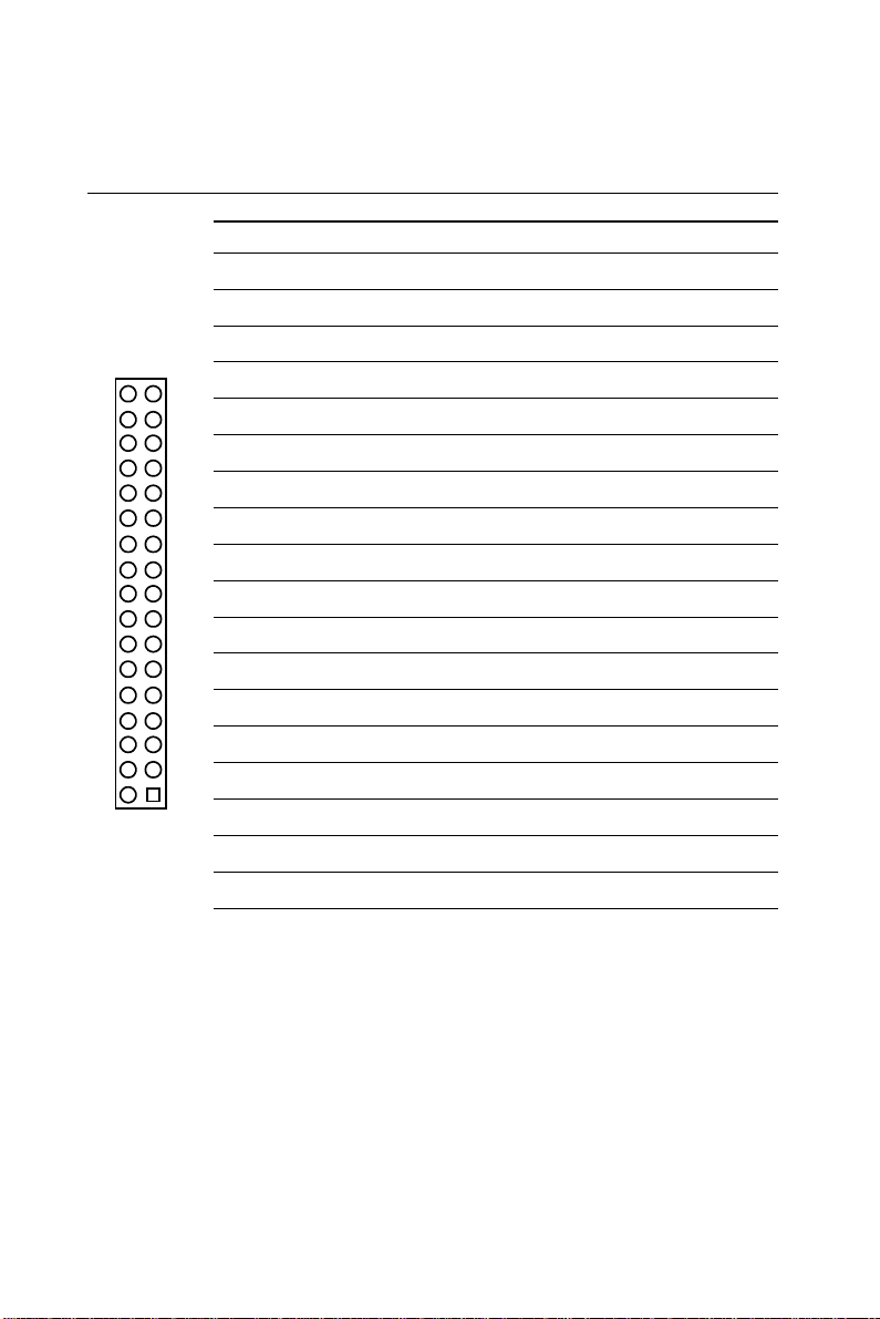
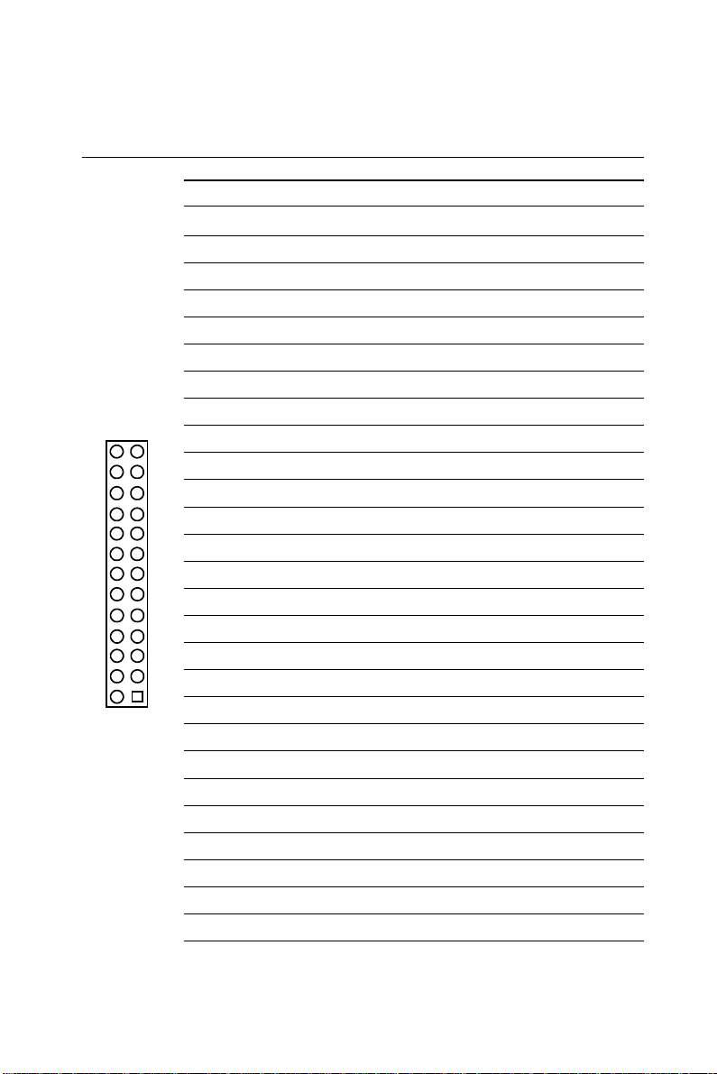
2.1 Board layout: Connector locations (component side)
CN27
CN8
CN3
CN20
CN28
CN18
CN22
CN23
CN12
CN21
CN17
CN14
CN15
CN16
CN13
CN10
CN11
CN9
CN4
CN25
CN26
VR2
CN5
CN1
CN6
CN7
CN2
VR1
16 PCA-6751 Series User's Manual

2.2 Board layout: Connector locations (solder side)
SODIMM BANK 1
CN24
SODIMM BANK 0
Chapter 2 Connecting Peripherals 17

The following table lists the connectors on the PCA-6751 Series.
Table 2-1: Connectors
Number Function
CN1 FDD connector
CN2 Parallel port connector
CN3 Keyboard lock, LED connector
CN4 USB connector
CN5 24-bit LCD display connector
CN6 36-bit LCD display connector
CN7 LCD inverter connector
CN8 IR connector
CN9 External speaker connector
CN10 Reserved
CN11 VGA connector
CN12 PC/104 connector
CN13 Ethernet connector
CN14 COM2 RS-422/485 connector
CN15 COM2 RS-232 connector
CN16 COM1 RS-232 connector
CN17 External keyboard connector
CN18 ATX power connector
CN19 Reserved
CN20 AT power connector
CN21 Keyboard and PS/2 mouse connector
CN22 ISA gold finger connector
CN23 ISA gold finger connector
CN24 CompactFlash™ card connector
CN25 HDD LED connector
CN26 System reset switch connector
CN27 ATX power button
CN28 Enhanced IDE connector
18 PCA-6751 Series User's Manual

The following sections tell how to make each connection. In most
cases, you will simply need to connect a standard cable. All of the
connector pin assignments are shown in Appendix C.
Warning! Always completely disconnect the power cord from
your chassis whenever you are working on it. Do not
make connections while the power is on. Sensitive
electronic components can be damaged by a
sudden rush of power. Only experienced electronics
personnel should open the PC chassis.
Caution! Always ground yourself to remove any static charge
before touching the CPU card. Modern electronic
devices are very sensitive to static electric charges.
Use a grounding wrist strap at all times. Place all
electronic components on a static-dissipative
surface or in a static-shielded bag when they are not
in the chassis.
2.3 FDD connector (CN1)
You can attach up to two floppy disk drives to the PCA-6751 Series’
onboard controller. You can use any combination of 5.25" (360 KB/
1.2 MB) and/or 3.5" (720 KB/1.44/2.88 MB) drives.
The card comes with a 34-pin daisy-chain drive connector cable. On
one end of the cable is a 34-pin flat-cable connector. On the other
end are two sets of floppy disk drive connectors. Each set consists of
a 34-pin flat-cable connector (usually used for 3.5" drives) and a
printed-circuit-board connector (usually used for 5.25" drives). You
can use only one connector in each set. The set on the end (after the
twist in the cable) connects to the A: floppy. The set in the middle
connects to the B: floppy.
Chapter 2 Connecting Peripherals 19

2.4 Parallel port connector (CN2)
The parallel port is normally used to connect the CPU card to a
printer. The PCA-6751 Series includes an on-board parallel port,
accessed through a 26-pin flat-cable connector, CN3. The card comes
with an adapter cable which lets you use a traditional DB-25 connector. The cable has a 26-pin connector on one end and a DB-25
connector on the other, mounted on a retaining bracket. The bracket
installs at the end of an empty slot in your chassis, giving you access
to the connector.
The parallel port is designated as LPT1, and can be disabled or
changed to LPT2 or LPT3 in the system BIOS setup.
To install the bracket, find an empty slot in your chassis. Unscrew the
plate that covers the end of the slot. Screw in the bracket in place of
the plate. Next, attach the flat-cable connector to CN2 on the CPU
card. Wire 1 of the cable is red or blue, and the other wires are gray.
Make sure that wire 1 corresponds to pin 1 of CN2. Pin 1 is on the
right side of CN2.
2.5 Keyboard lock, LED connector (CN3)
Connecting CN3 enables the keyboard locking function from the front
panel of your chassis.
2.6 USB connector (CN4)
The PCA-6751 Series board provides two USB (Universal Serial Bus)
interfaces, which give complete plug and play and also hot
attach/detach for up to 127 external devices. The USB interfaces
comply with USB specification rev. 1.0 and are fuse protected.
The USB interfaces are accessed through a 10-pin flat-cable connector, CN9. The adapter cable has a 10-pin connector on one end and a
USB connector on the bracket.
The USB interfaces can be disabled in the system BIOS setup.
20 PCA-6751 Series User's Manual

2.7 24-bit LCD display connector (CN5)
CN5 is a 40-pin dual-in-line header and is used to connect an LCD
display to the PCA-6751 Series. The PCA-6751 Series has bias
control which can be used to control the LCD signal voltage. Pin 7 of
CN5 is for LCD contrast adjustments, the LCD contrast can be
adjusted via the VR2 (located on the upper left corner of CN5).
The VGA interface is set up solely with the software utiliity provided.
Refer to Chapter 4 for details.
2.8 36-bit LCD display connector (CN6)
The PCA-6751 Series supports 36-bit LCD that must be connected to
both CN5 (40-pin) and CN6 (20-pin).
The pin assignments for both CN5 and CN6 can be found in
Appendix C.
2.9 LCD inverter connector (CN7)
The LCD inverter is connectoed to CN7 via a 5-pin connector to
provide +12 V power to the LCD display. Pin 4 of CN7 provides LCD
brightness control and can be adjusted via the VR1 (located on the
uppper right corner of CN7).
2.10 IR connector (CN8)
This connector supports the optional wireless infrared transmitting
and receiving module. This module mounts on the system case. You
must configure the setting through BIOS setup.
2.11 External speaker connector (CN9)
Connect external speakers to CN9. To activate the on-board buzzer,
set the connector so that Pins 4 and 5 are closed.
Chapter 2 Connecting Peripherals 21

2.12 VGA display connector (CN11)
The PCA-6751 Series provides a VGA controller for a high resolution
VGA interface. The PCA-6751Series' CN7 is a DB-15 connector for
VGA monitor input. Pin assignments for the CRT display are detailed
in Appendix C.
2.13 PC/104 connectors (CN12)
The PCA-6751 Series is equipped with a 16-bit ISA signal PC/104
connector for future expansion. See Appendix B for details.
2.14 Ethernet connector (CN13) (PCA-6751 only)
The PCA-6751 is equipped with a high performance 32-bit PCI-bus
Fast Ethernet interface which is fully compliant with IEEE 802.3u
100/10Base-T specifications. It is supported by all major network
operating systems.
The medium type can be configured via the Intel82558.EXE program
included on the utility disk. (See Chapter 5 for detailed information.)
2.14.1 RJ-45A connector (CN13)
100/10Base-T connects to the PCA-6751 via an adapter cable to the
RJ-45 standard jack.
2.14.2 Network boot
The network boot feature is built into the BIOS. It can be enabled or
disabled in the chipset setup of the CMOS configuration. Refer to
"BIOS Setting" in Chapter 4 for more information.
22 PCA-6751 Series User's Manual

2.15 Serial ports (CN16: COM1; CN15: COM2/RS-232; CN14: COM2/RS-422/485)
The PCA-6751 Series offers two serial ports: COM1 in RS-232 and
COM2 (CN15: RS-232, CN14:RS-422/485). These ports let you
connect to serial devices (a mouse, printers, etc.) or a communication
network.
You can select the address for each port (for example, 3F8H [COM1],
2F8H [COM2]) or disable each port. Use the BIOS Advanced Setup
program, which is covered in Chapter 4.
The card mounting bracket holds the serial port connector for the one
port. The parallel port and serial port adapter kit (supplied with the
card) holds the connector for the other port. This lets you connect and
disconnect cables after you install the card. The DB-9 connector on
the bottom of the bracket is the first RS-232 port, COM1. The DB-9
connector on the adapter kit is the second serial port, COM2.
Table 2-2: Serial port connections (COM1, COM2)
Connector Function
COM1 RS-232
COM2 RS-232/422/485
2.15.1 RS-232 connection (COM1: CN16)
Different devices implement the RS-232 standard in different ways. If
you are having problems with a serial device, be sure to check the pin
assignments for the connector.
Chapter 2 Connecting Peripherals 23

2.15.2 RS-232/422/485 connection (COM2: CN15: RS-232; CN14: RS-422/485)
COM2 is an RS-232/422/485 serial port. The specific port type is
determined by jumper settings (JP1), as detailed in Chapter 1.
The IRQ and address range for both ports are fixed. However, if you
wish to disable the port or change these parameters later, you can do
this in the system BIOS setup. The table below shows the settings for
the PCA-6751 Series' board's ports:
Table 2-3: Serial port default settings
Port Address Interrupt Default
COM1 3F8, 3E8 IRQ4 3F8
COM2 2F8, 2E8 IRQ3 2F8
2.16 External keyboard connector (CN17)
In addition to the PS/2 mouse/keyboard connector, an additional
external keyboard connector is provided.
For external keyboard pin assignments, see Appendix D.
2.17 ATX power connector (CN18)
If the PCA-6751 Series is used as a standalone card, both the 4-pin
main power connector (CN20) and the ATX power connector (CN18)
must be connected to the power supply. If the PCA-6751 Series is
used with a passive backplane, the main power connector (CN20)
should not be connected as the card will be powered from the backplane.
Use the ATX adapter cable (provided) to connect the PCA-6751
Series with the ATX power supply. The ATX adapter cable has two
different connectors at either end. The ATX 20-pin (female type)
connects to the power supply, while the 3-pin (female type) connects
to the ATX power connector (CN18) on the board itself.
24 PCA-6751 Series User's Manual

2.18 AT power connector (CN20)
If you prefer not to acquire power through PCA-6751 Series' backplane via the gold H-connectors, CN20 also provides power input
connectors for +5 V, -12 V and +12 V. Pin 8 of the PS/2 power
supply can be used, too.
2.19 Keyboard and PS/2 mouse connector (CN21)
The PCA-6751 Series' board provides a keyboard connector. A 6-pin
mini-DIN connector (CN21) on the card mounting bracket supports
single-board computer applications. The card comes with an adapter
to convert from the 6-pin mini-DIN connector to a standard DIN
connector and to a PS/2 mouse connector.
2.20 ISA gold fingers (CN22, CN23)
The 16-bit ISA gold fingers are used for connecting the PCA-6751
Series to an ISA passive backplane.
2.21 CompactFlash™ disk (CN24)
The PCA-6751 Series is equipped with a CompactFlash™ disk socket
on the solder side that supports the IDE interface for CompactFlash
cards. The onboard CompactFlash™ socket is designed to prevent
incorrect installation. Make sure that the system power is off when
installing and removing CompactFlash™ cards.
The CompactFlash™ card is defaulted as the E drive on your
PC.system.
Chapter 2 Connecting Peripherals 25

2.22 Front panel connector (CN25, CN26, CN27)
Next, you may want to install external switches to monitor and control
the PCA-6751 Series. These features are optional - install them only if
you need them. The front panel connector provides connections for
both a speaker and a hard disk access indicator, and it also provides an
input switch for resetting the card and the ATX system power switch.
2.22.1 Hard disk drive LED (CN25)
You can connect an LED to connector CN25 to indicate when the
HDD is active. Marks on the circuit board indicate LED polarity.
2.22.2 Reset switch (CN26)
If you install a reset switch, it should be a single pole switch rated at
10 mA, 5 V. Momentarily pressing the switch will activate a reset.
For reset switch pin assignments, please see Appendix C.
2.22.3 ATX power button (CN27)
The PCA-6751 Series provides an ATX power input connector. When
connected with the ATX power switch, the ATX power switch
connector (CN27) enables power On/Off from the chassis.
26 PCA-6751 Series User's Manual

2.23 Enhanced IDE connector (CN28)
You can attach two IDE (Integrated Device Electronics) drives to the
PCA-6751 Series' internal controller. The PCA-6751 Series CPU card
has an EIDE connector, CN28.
Wire number 1 on the cable is red or blue, and the other wires are
gray. Connect one end to connector CN28 on the CPU card. Make
sure that the red (or blue) wire corresponds to pin 1 on the connector
(on the right side). See Chapter 1 for help in finding the connector.
Unlike floppy drives, IDE hard drives can connect in either position
on the cable. If you install two drives, you will need to set one as the
master and one as the slave. You do this by setting the jumpers on the
drives. If you use just one drive, you should set it as the master. See
the documentation that came with your drive for more information.
Connect the first hard drive to the other end of the cable. Wire 1 on
the cable should also connect to pin 1 on the hard drive connector,
which is labeled on the drive circuit board. Check the documentation
that came with the drive for more information.
Connect the second drive, as described above, on CN28.
Chapter 2 Connecting Peripherals 27
2.24 ATX Feature Connector (CN27)
When the PCA-6751 is used as a standalone card, both the main
power connector (CN20) and the ATX feature connector (CN27) must
be connected to the power supply. If the PCA-6751 is used with a
passive backplane, the main power connector (CN20) should not be
connected. This is because the card will be powered from the backplane.
To ATX feature
connector (CN27)
ATX power supply source
(P8) 6-pin in backplane
(P9) 6-pin in backplane
P8
P9P8P9
20-pin female connector
Figure 2-4: ATX adaptor cable
The ATX adapter cable (provided) is used to connect the PCA-6751
to the ATX power supply. The ATX adapter cable has different
connectors at both ends. On one end is the ATX 20-pin (female type)
which connects to the (male) ATX power supply source. The other
end has a 3-pin connector (female type) which connects to the ATX
feature connector (CN27) on the board itself. This end also has the
6-pin main power connector (P8) and a 6-pin connector (P9) which is
used when the board is mounted on a passive backplane.
28 PCA-6751 Series User's Manual

CHAPTER
3
Award BIOS Setup
This chapter describes how to set the
card’s BIOS configuration data.

3.1 Introduction
Figure 3-1: Setup program initial screen
Award’s BIOS ROM has a built-in Setup program that allows users to
modify the basic system configuration. This type of information is
stored in battery-backed RAM so that it retains the Setup information
when the power is turned off.
3.2 Entering setup
Turning on the computer and pressing <DEL> immediately will allow
you to enter Setup.
30 PCA-6751 Series User's Manual

3.3 Standard CMOS setup
Choose the “STANDARD CMOS SETUP” option from the INITIAL
SETUP SCREEN Menu, and the screen below is displayed. This
standard Setup Menu allows users to configure system components
such as date, time, hard disk drive, floppy drive, display, and memory.
Figure 3-2: CMOS setup screen
Chapter 3 Award BIOS Setup 31

3.4 BIOS features setup
The “BIOS FEATURES SETUP” screen appears when choosing the
BIOS FEATURES SETUP item from the CMOS SETUP UTILITY
Menu. It allows the user to configure the PCA-6751 Series according
to his particular requirements.
Below are some major items that are provided in the BIOS FEATURES SETUP screen:
Figure 3-3: BIOS features setup screen
Virus Warning
During and after the system boots up, any attempt to write to the boot
sector or partition table of the hard disk drive will halt the system. In
this case, a warning message will be displayed. You can run the antivirus program to locate the problem.
If Virus Warning is Disabled, no warning message will appear if
anything attempts to access the boot sector or hard disk partition.
CPU Internal Cache/External Cache
Depending on the CPU/chipset design, these options can speed up
memory access when enabled.
32 PCA-6751 Series User's Manual

Quick Power On Self Test
This option speeds up the Power-On Self Test (POST) conducted as
soon as the computer is turned on. When enabled, BIOS shortens or
skips some of the items during the test. When disabled, normal POST
procedures assumes.
Boot Sequence
This function determines the sequence in which the computer will
search the drives for the disk operating system (i.e. DOS). The default
value is “C, A”.
A,C System will first search the FDD, then the HDD.
C,A System will first search the HDD, then the FDD.
C only System will only search the HDD.
• •
• •
• •
Boot Up Floppy Seek
During POST, BIOS will determine if the floppy disk drive installed is
40 or 80 tracks. 360 KB type is 40 tracks while 720 KB, 1.2 MB, and
1.44 MB are all 80 tracks.
Enabled BIOS searches the floppy drive to determine if it is 40 or 80
tracks. Note that BIOS cannot differentiate 720 KB, 1.2 MB,
and 1.44 MB type drives as they are all 80 tracks.
Disabled BIOS will not search for the floppy drive type by track
number. Note that there will not be any warning message if
the drive installed is 360 KB.
Boot Up NumLock Status
The default is “On”.
On Keypad boots up to number keys.
Off Keypad boots up to arrow keys.
Chapter 3 Award BIOS Setup 33

Boot Up System Speed
High Sets the speed to high
Low Sets the speed to low
IDE HDD Block Mode
Enabled Enable IDE HDD Block Mode. BIOS will detect the block size
of the HDD and send a block command automatically.
Disabled Disable IDE HDD Block Mode
Gate A20 option
Normal The A20 signal is controlled by the keyboard controller or
chipset hardware
Fast Default: Fast. The A20 signal is controlled by Port 92 or
chipset specific method.
Typematic Rate Setting
The typematic rate determines the characters per second accepted by
the computer. Typematic Rate setting enables or disables the typematic rate.
Typematic Rate (Char/Sec)
BIOS accepts the following input values (character/second) for
Typematic Rate: 6, 8, 10, 12, 15, 20, 24, 30.
Typematic Delay (msec)
When holding down a key, the Typematic Delay is the time interval
between the appearance of the first and second characters. The input
values (msec) for this category are: 250, 500, 750, 1000.
34 PCA-6751 Series User's Manual

Security Option
This setting determines whether the system will boot if the password
is denied, while limiting access to Setup.
System The system will not boot, and access to Setup will be
denied if the correct password is not entered at the prompt.
Setup The system will boot, but access to Setup will be
denied if the correct password is not entered at the prompt.
Note: To disable security, select PASSWORD SETTING in the main
menu. At this point, you will be asked to enter a password. Simply hit
the <ENTER> key to disable security. When security is disabled, the
system will boot, and you can enter Setup freely.
OS Select for DRAM>64 MB
This setting is under OS/2 system.
Video BIOS Shadow
This determines whether video BIOS will be copied to RAM, which is
optional according to the chipset design. When enabled, Video
Shadow increases the video speed.
C8000 - CFFFF Shadow/DC000-DFFFF Shadow
These determine whether optional ROM will be copied to RAM in
blocks of 16 KB.
Enabled Optional shadow is enabled
Disabled Optional shadow is disabled
Chapter 3 Award BIOS Setup 35

3.5 Chipset features setup
By choosing the “CHIPSET FEATURES SETUP” option from the
INITIAL SETUP SCREEN Menu, the screen below is displayed. This
sample screen contains the manufacturer’s default values for the
PCA-6751 Series.
Figure 3-4: Chipset features setup screen
36 PCA-6751 Series User's Manual

3.6 Power management setup
The power management setup controls the CPU cards’ “green”
features. The following screen shows the manufacturer’s default.
Figure 3-5: Power management setup screen
Power Management
This option allows you to determine if the values in power management are disabled, user-defined, or predefined.
HDD Power Management
You can choose to turn the HDD off after a one of the time interval
listed, or when the system is in Suspend mode. If in a power saving
mode, any access to the HDD will wake it up.
Note: HDD will not power down if the Power Management
option is disabled.
IRQ Activity
IRQ can be set independently. Activity on any enabled IRQ will wake
up the system.
Chapter 3 Award BIOS Setup 37

3.7 PnP PCI configuration setup
Figure 3-6: PCI configuration screen
3.8 Load BIOS defaults
“LOAD BIOS DEFAULTS” indicates the most appropriate values for
the system parameters for minimum performance. These default
values are loaded automatically if the stored record created by the
Setup program becomes corrupted (and therefore unusable).
3.9 Load setup defaults
“LOAD SETUP DEFAULTS” loads the values required by the
system for maximum performance.
38 PCA-6751 Series User's Manual

3.10 Integrated peripherals
Figure 3-7: Integrated peripherals
Note: If you enable the IDE HDD block mode, the en-
hanced IDE driver will be enabled.
3.11 Password setting
To change, confirm, or disable the password, choose the “PASSWORD SETTING” option form the Setup main menu and press
[Enter]. The password can be at most 8 characters long.
Remember, to enable this feature. You must first select the Security
Option in the BIOS FEATURES SETUP to be either “Setup” or
“System.” Pressing [Enter] again without typing any characters can
disable the password setting function.
Chapter 3 Award BIOS Setup 39

3.12 IDE HDD auto detection
“IDE HDD AUTO DETECTION” automatically self-detects for the
correct hard disk type.
3.13 Save & exit setup
If you select this and press the [Enter] key, the values entered in the
setup utilities will be recorded in the CMOS memory of the chipset.
The microprocessor will check this every time you turn your system
on and compare this to what it finds as it checks the system. This
record is required for the system to operate.
3.14 Exit without saving
Selecting this option and pressing the [Enter] key lets you exit the
Setup program without recording any new values or changing old
ones.
40 PCA-6751 Series User's Manual

CHAPTER
PCI SVGA Setup
• Introduction
• Installation of SVGA driver
- for Windows 3.1
- for Windows 95
- for Windows NT
• Further information
4

4.1 Introduction
The PCA-6751 Series has an onboard PCI flat panel/VGA interface.
The specifications and features are described as follows:
4.1.1 Chipset
The PCA-6751 Series uses a C&T 69000/69030 chipset for its
PCI/SVGA controller. It supports many popular LCD, EL, and gas
plasma flat panel displays and conventional analog CRT monitors.
The 6900/69030 VGA BIOS supports monochrome LCD, EL, color
TFT and STN LCD flat panel displays. In addition, it also supports
interlaced and non-interlaced analog monitors (color and monochrome VGA) in high-resolution modes while maintaining complete
IBM VGA compatibility. Digital monitors (i.e. MDA, CGA, and
EGA) are NOT supported. Multiple frequency (multisync) monitors
are handled as if they were analog monitors.
4.1.2 Display memory
With on-board 2 MB display memory, the VGA controller can drive
CRT displays or color panel displays with resolutions up to 1024 x
768 at 64 K colors. The display memory can be expanded to 4 MB for
true-color resolution of 1024 x 768 with C&T 69030.
4.1.3 Display types
CRT and panel displays can be used simultaneously. The PCA-6751
Series can be set in one of three configurations: on a CRT, on a flat
panel display, or on both simultaneously. The system is initially set to
simultaneous display mode. The utility disks includes three *.COM
files in the subdirectory Utility\vga\ which can be used to
configure the display. In order to use these configuration programs,
type the file name and path at the DOS prompt.
CT.COM: Enables CRT display only
FP.COM: Enables panel display only
SM.COM: Enables both displays simultaneously
42 PCA-6751 Series User's Manual

4.2 Installation of SVGA driver
Complete the following steps to install the SVGA driver. Follow the
procedures in the flow chart that apply to the operating system that you
you are using within your PCA-6751 Series.
Important: The following windo ws illustrations are e xamples only.
You must follow the flow chart instructions and pay
attention to the instructions which then appear on your
screen.
Note: <Enter> means pressing the “Enter” key on the
keyboard.
Chapter 4 PCI SVGA Setup 43
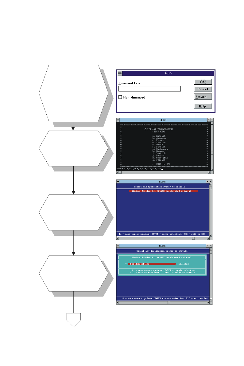
4.2.1 Installation for Windows 3.1
a. Insert the utility
disc into the
CD-ROM drive.
1.
2.
3.
b. Select "File" in
Program Manager.
c. Click "Run" and
type: D:\SlotPC\
6751\VGA\69000\
Win31
a. Choose the
language you want
to use during
installation.
a. Select the
highlighted item.
b. Press "ENTER".
D:\SlotPC\6751\VGA\69000\Win31
a. Press "ENTER" to
4.
44 PCA-6751 Series User's Manual
install all
resolutions.
5.
6.
7.
a. Type the path of
the operating
system.
a. When installation
is completed,
reboot the system.
b. You will see the
"ChipsCPL" icon in
the control panel.
a. Double click
"ChipsCPL".
b. Adjust screen size,
color and refresh
rate to your
preferences.
ChipsCPL
END
Chapter 4 PCI SVGA Setup 45
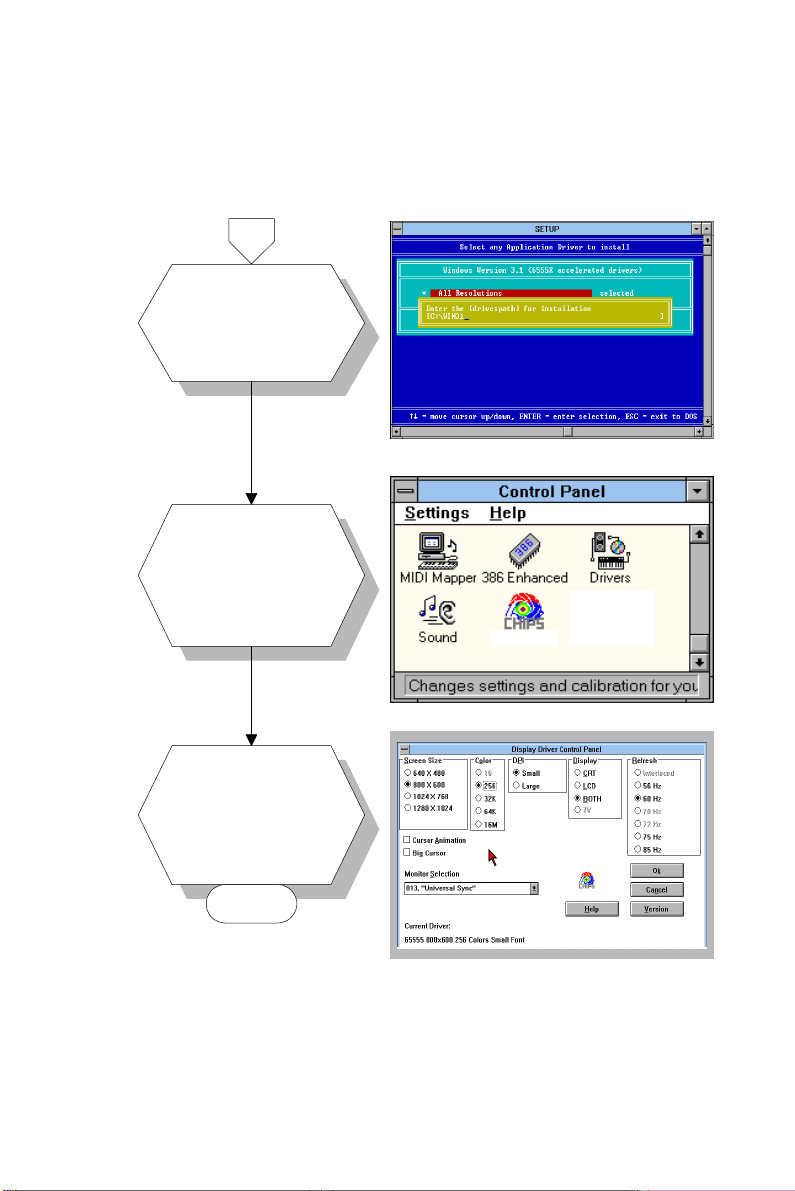
4.2.2 Installation for Windows 95
a. Select "Start",
"Settings" ,
"Control Panel" ,
1.
2.
"Display" ,
"Settings".
b. Press "Advanced
Properties".
a. Choose the
"Adapter" label.
b. Press the
"Change..."
button.
3.
4.
46 PCA-6751 Series User's Manual
a. Press the "Have
Disk" button.
a. Insert the utility
disc into the
CD-ROM drive.
b. Type: D:\SlotPC\
6751\VGA\69000\
Win95
c. Press "OK".
D:\SlotPC\6751\VGA\69000\Win95

5.
6.
a. Select the
highlighted item.
b. Click the "OK"
button.
a. C&T69000/69030
appears in the
adapter label.
b. Click the "Apply"
button.
69000
69000
7.
8.
a. Press "Yes" to
reboot.
a. Repeat Step 1 on
the previous page
of this manual.
The "CHIPS"
label appears in
"Display".
b. Adjust resolution
and color.
Chapter 4 PCI SVGA Setup 47
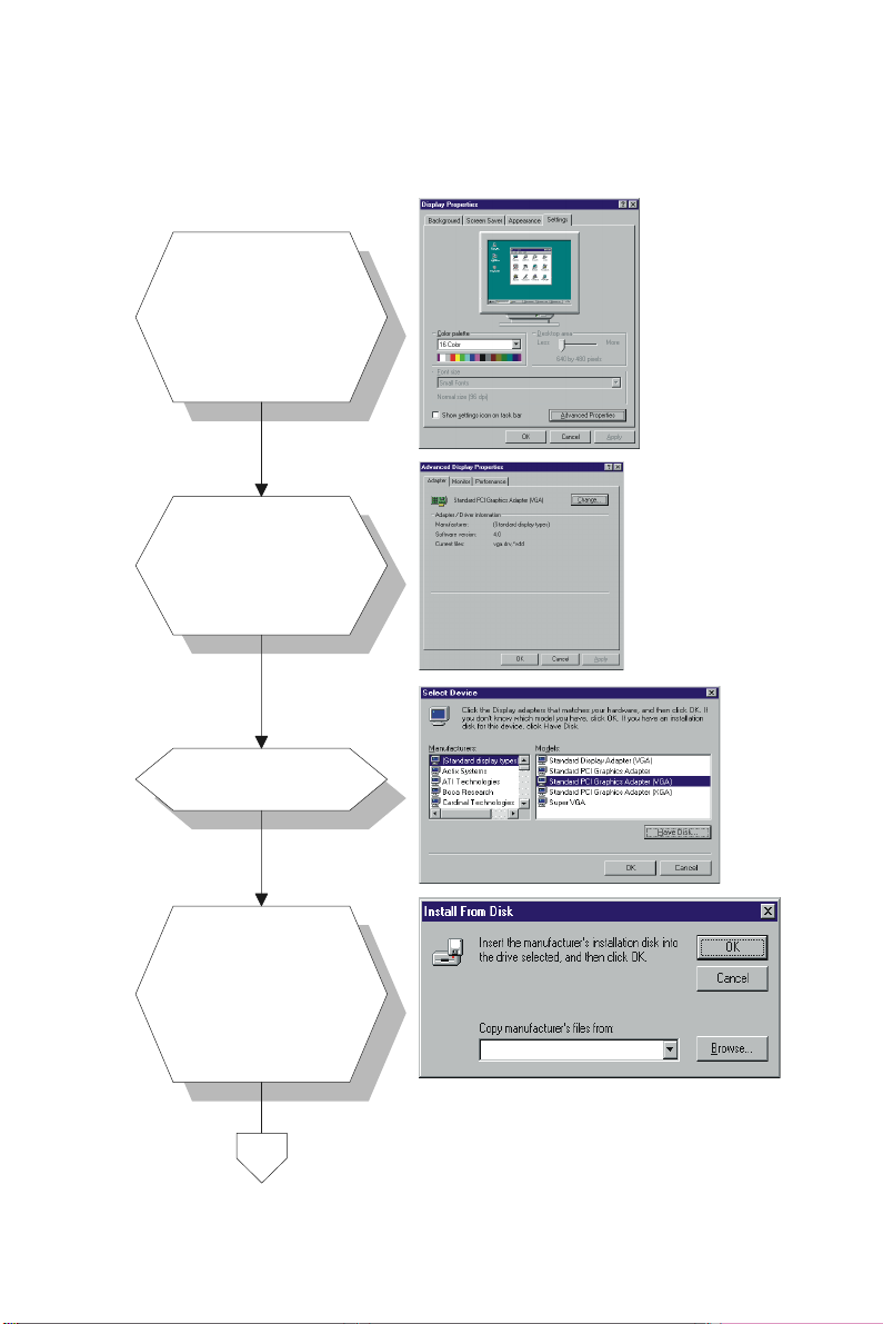
9.
10.
11.
a. Click the "CHIPS"
label.
b. Adjust the refresh
rate and display
type.
c. Press "OK" to
exit.
a. Press "Yes" to
set the monitor
type.
a. Select
"Standard",
"Super VGA 800
x 600", or "XGA".
b. Press the "OK"
button.
[7]
12.
48 PCA-6751 Series User's Manual
a. Choose "Restart"
to reboot.
END

4.2.3 Installation for Windows NT
a. Select "Start", "Settings",
1.
2.
"Control Panel".
b. Double click the "Display"
icon.
a. Choose the "Settings" label.
b. Press the "Display Type"
button.
3.
4.
a. Press the "Change..." button.
a. Click the "Have Disk..."
button.
Chapter 4 PCI SVGA Setup 49

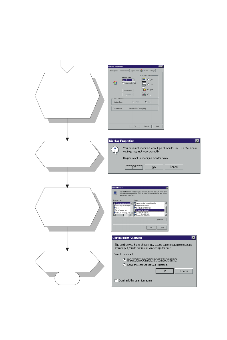
5.
6.
a. Insert the utility disc into
the CD-ROM drive.
b. Type D:\SlotPC\6751\
VGA\NT40\
c. Press the "OK" button.
D:\SlotPC\6751\VGA\NT40\
a. Select the highlighted
item.
b. Press the "OK" button.
7.
8.
50 PCA-6751 Series User's Manual
a. Press "Yes" to proceed.
a. Press "OK" to reboot.

9.
a. Repeat Step 1 in this
manual, to select the
"Settings" label.
b. Adjust resolution and color.
c. Click "Test" to see the
result.
d. Click "OK" to save the
setting.
END
Chapter 4 PCI SVGA Setup 51

4.3 Further information
For more information about the PCI/SVGA installation in your
PCA-6751 Series, including driver updates, troubleshooting guides
and FAQ lists, visit the following web resources:
C&T website: www.chips.com
Advantech websites: www.advantech.com
www.advantech.com/support
52 PCA-6751/6751V Series User's Manual

CHAPTER
5
PCI Bus Ethernet
Interface With Intel
SB82558/SB82559
(PCA-6751 only)
This chapter provides information on
Ethernet configuration.
• Introduction
• Installation of Ethernet driver
- Installation for MS-DOS and
Windows 3.1
- Installation for Windows 95
- Installation for Windows NT
• Further information
®

5.1 Introduction
The PCA-6751 is equipped with a high performance 32-bit Ethernet
chipset which is fully compliant with IEEE 802.3 100 Mbps
CSMA/CD standards. It is supported by major network operating
systems. It is also both 100Base-T and 10Base-T compatible. The
medium type can be configured via the 82558.exe program included
on the utility disk.
The Ethernet port provides a standard RJ-45 jack. The network boot
feature can be utilized by incorporating the boot ROM image files for
the appropriate network operating system. The boot ROM BIOS files
are combined with system BIOS, which can be enabled/disabled in the
BIOS setup.
5.2 Installation of Ethernet driver
Before installing the Ethernet driver, note the procedures below. You
must know which operating system you are using in your PCA-6751,
and then refer to the corresponding installation flow chart. Then just
follow the steps described in the flow chart. You will quickly and
successfully complete the installation, even if you are not familiar
with instructions for MS-DOS or WINDOWS.
Note 1: The windows illustr ations in this chapter are e xam-
ples only. You must follow the flow chart instructions
and pay attention to the instructions which then
appear on your screen.
5.2.1 Installation for MS-DOS and Windows 3.1
If you want to set up your Ethernet connection under the MS-DOS or
Windows 3.1 environment, you should first check your server system
model. For example, MS-NT, IBM-LAN server, and so on.
Then choose the correct driver to install in your panel PC.
The installation procedures for various servers can be found in the
directory path "LAN/TXT/*" of the drivers and utilities disks, where *
is your server model.
54 PCA-6751 Series User's Manual

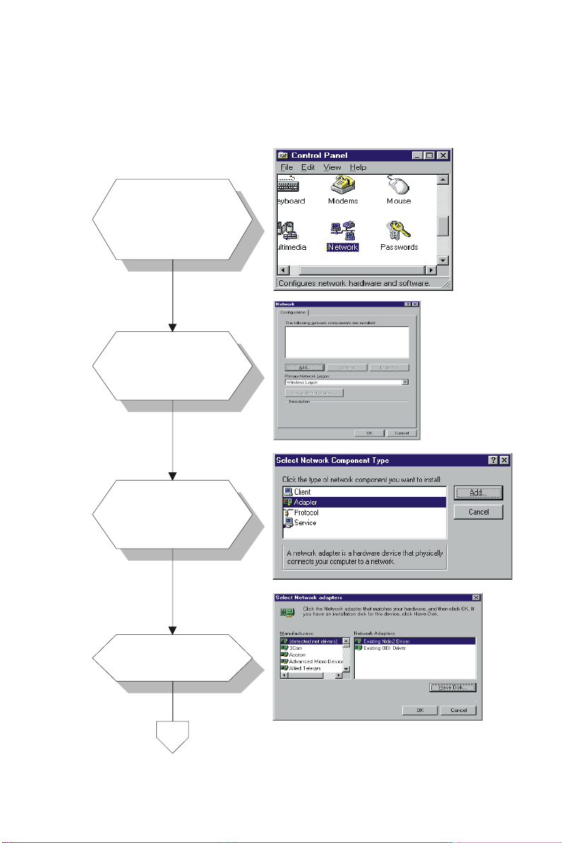
5.2.2 Installation for Windows 95
a. Select "Start",
"Settings",
1.
2.
3.
"Control Panel".
b. Double click
"Network".
a. Click "Add" and
prepare to install
network functions.
a. Select the
"Adapter" item to
add the Ethernet
card.
4.
a. Click "Have Disk"
to install the driver.
Chapter 5 PCI Bus Ethernet Interface With Intel® SB82558/SB82559 (PCA-6751 only) 55
5.
6.
7.
a. Insert the utility
disc into the
CD-ROM drive.
Type: D:\SlotPC\
b.
6751\Ether.100\
82558\Win95\
Setup.exe
c. Click "OK".
a. Choose the "Intel"
item.
b. Click "OK".
a. Make sure the
configurations of the
relevant items are
set correctly.
b. Click "OK" to
reboot.
D:\SlotPC\6751\Ether.100\82558\Win95\Setup.exe
END
56 PCA-6751 Series User's Manual

5.2.3 Installation for Windows NT
a. Select "Start",
"Settings",
1.
2.
"Control Panel".
b. Double click
"Network".
a. Choose the
"Adapters" label.
b. Click the "Add"
button.
3.
4.
Chapter 5 PCI Bus Ethernet Interface With Intel® SB82558/SB82559 (PCA-6751 only) 57
a. Press "Have
Disk".
a. Type "D:".
b. Press "OK".
D:

5.
6.
7.
a. Insert the utility
disc into the
CD-ROM drive.
Type: D:\SlotPC\
b.
6751\Ether.100\
82558\Winnt\
Click "OK".
c.
a. Choose the
"Realtek" item.
b. Click "OK".
a. Make sure the
configurations of
relevant items are
set correctly.
b. Click "OK" to
reboot.
D:\SlotPC\6751\Ether.100\82558\Winnt\
END
58 PCA-6751 Series User's Manual

5.3 Further information
Intel® website: www.intel.com
Advantech websites: www.advantech.com
www.advantech.com/support
Chapter 5 PCI Bus Ethernet Interface With Intel® SB82558/SB82559 (PCA-6751 only) 59

60 PCA-6751 Series User's Manual

CHAPTER
6
PCI Bus Ethernet
Interface With
RTL-8139
(PCA-6751 only)
This chapter provides information on
Ethernet configuration.
• Introduction
• Installation of Ethernet driver
- for Windows 95/98
- for Windows NT
• Further information

6.1 Introduction
The PCA-6751 is equipped with a high performance 32-bit Ethernet
chipset which is fully compliant with IEEE 802.3 100 Mbps CSMA/
CD standards. It is supported by major network operating systems. It
is also both 100Base-T and 10Base-T compatible. The medium type
can be configured via the RSET8139.exe program included on the
utility disk.
The Ethernet port provides a standard RJ-45 jack on board. The
network boot feature can be utilized by incorporating the boot ROM
image files for the appropriate network operating system. The boot
ROM BIOS files are combined with system BIOS, which can be
enabled/disabled in the BIOS setup.
6.2 Installation of Ethernet driver
Before installing the Ethernet driver, note the procedures below. You
must know which operating system you are using in your PCA-6751,
and then refer to the corresponding installation flow chart. Then just
follow the steps described in the flow chart. You will quickly and
successfully complete the installation, even if you are not familiar
with instructions for MS-DOS or Windows.
Note: The windows illustrations in this chapter are exam-
ples only. You must follow the flow chart instructions
and pay attention to the instructions which then
appear on your screen.
6.2.1 Installation for MS-DOS and Windows 3.1
If you want to set up your Ethernet connection under the MS-DOS or
Windows 3.1 environment, you should first check your server system
model. For example, MS-NT, IBM-LAN server, and so on.
Then choose the correct driver to install in your panel PC.
The installation procedures for various servers can be found on
CD-ROM. The file path is: D:\SlotPC\6751\Ethernet\8139\wfw311
62 PCA-6751 Series User's Manual
6.2.2 Installation for Windows 95/98
a. Select "Start",
"Settings",
1.
2.
3.
"Control Panel".
b. Double click
"Network".
a. Click "Add" and
prepare to install
network functions.
a. Select the
"Adapter" item to
add the Ethernet
card.
4.
a. Click "Have Disk"
to install the driver.
Chapter 6 PCI Bus Ethernet Interface With RTL-8139 (PCA-6751 only) 63
5.
6.
7.
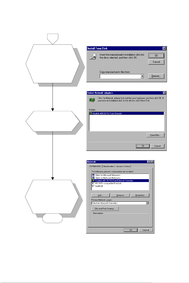
Insert the utility
a.
disc into the
CD-ROM drive.
Type: D:\SlotPC\
b.
6751\Ethernet\8139\
Win95\
c. Click "OK".
a. Choose the
"Realtek" item.
b. Click "OK".
a. Make sure the
configurations of
relevant items are
set correctly.
b. Click "OK" to
reboot.
D:\SlotPC\6751\Ethernet\8139\Win95\
END
Note: The correct path for Windo ws 98 is:
D:\SlotPC\6751\Ethernet\8139\Win98\
64 PCA-6751 Series User's Manual

6.2.3 Installation for Windows NT
a. Select "Start",
"Settings",
1.
2.
"Control Panel".
b. Double click
"Network".
a. Choose the
"Adapters" label.
b. Click the "Add"
button.
3.
4.
a. Press "Have
Disk".
a. Insert the utility
disc into the
CD-ROM drive.
Type: D:\SlotPC\
b.
6751\Ethernet\8139\
Winnt\
Click "OK".
c.
Chapter 6 PCI Bus Ethernet Interface With RTL-8139 (PCA-6751 only) 65
D:\SlotPC\6751\Ethernet\8139Winnt\

5.
6.
a. Choose the
"Realtek" item.
b. Click "OK".
a. Make sure the
configurations of
relevant items are
set correctly.
b. Click "OK" to
reboot.
END
66 PCA-6751 Series User's Manual

6.3 Further information
Realtek website: www.realtek.com
Advantech websites: www.advantech.com
www.advantech.com/support
Chapter 6 PCI Bus Ethernet Interface With RTL-8139 (PCA-6751 only) 67

68 PCA-6751 Series User's Manual

APPENDIX
A
Programming the
Watchdog Timer
The PCA-6751 Series is equipped with a
watchdog timer that resets the CPU or
generates an interrupt if processing comes
to a standstill for any reason. This feature
ensures system reliability in industrial
standalone or unmanned environments.

A.1 Programming the watchdog timer
To program the watchdog timer, you must write a program which
writes I/O port address 443 (hex). The output data is a value of time
interval. The value range is from 01 (hex) to 3E (hex), and the related
time interval is 1 sec. to 62 sec.
Data Time Interval
01 1 sec.
02 2 sec.
03 3 sec.
04 4 sec.
••
••
••
3E 62 sec.
70 PCA-6751 Series User's Manual

After data entry, your program must refresh the watchdog timer by
rewriting the I/O port 443 (hex) while simultaneously setting it. When
you want to disable the watchdog timer, your program should read I/O
port 443 (hex).
The following example shows how you might program the watchdog
timer in BASIC:
10 REM Watchdog timer example program
20 OUT &H443, data REM Start and restart the watchdog
30 GOSUB 1000 REM Your application task #1,
40 OUT &H443, data REM Reset the timer
50 GOSUB 2000 REM Your application task #2,
60 OUT &H443, data REM Reset the timer
70 X=INP (&H443) REM, Disable the watchdog timer
80 END
1000 REM Subroutine #1, your application task
••
••
••
1070 RETURN
2000 REM Subroutine #2, your application task
••
••
••
2090 RETURN
Appendix A Programming the Watchdog Timer 71

72 PCA-6751 Series User's Manual

APPENDIX
B
Installing PC/104
Modules
This appendix gives instructions for
installing PC/104 modules.

B.1 Installing PC/104 modules
The PCA-6751 Series' PC/104 connectors give you the flexibility to
attach PC/104 modules.
Installing these modules on the PCA-6751 Series is quick and simple.
The following steps show how to mount the PC/104 modules:
1. Remove the PCA-675 Series from your system paying particular
attention to the safety instructions already mentioned above.
2. Make any jumper or link changes required to the CPU card now.
Once the PC/104 module is mounted you may have difficulty in
accessing these.
3. Normal PC/104 modules have male connectors and mount directly
onto the main card. (Refer to the diagram on the following page.)
4. Mount the PC/104 module onto the CPU card by pressing the
module firmly but carefully onto the mounting connectors.
5. Secure the PC/104 module onto the CPU card using the four
mounting spacers and screws.
74 PCA-6751 Series User's Manual
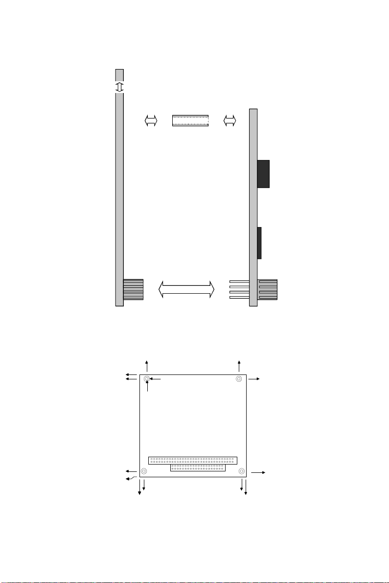
PC/104
Mounting Support
Female
PCA-6751 Series
Male
PC/104 module
Figure B-1: PC/104 module mounting diagram
95.9
90.8
5.1
8.9
φ
6.4
φ
3.2
0
5.1
0
82.5
85.1
90.8
5.1
90.2
Figure B-2: PC/104 module dimensions (mm) (±0.1)
Appendix B Installing PC/104 Modules 75

Table B-1: PCA-6751 Series PC/104 connectors (CN12)
Pin Signal (CN12)
Number Row A Row B Row C Row D
0 —— 0 V 0 V
1 IOCHCHK* 0 V SBHE* MEMCS16*
2 SD7 RESETDRV LA23 IOCS16*
3 SD6 +5 V LA22 IRQ10
4 SD5 IRQ9 LA21 IRQ11
5 SD4 -5 V LA20 IRQ12
6 SD3 DRQ2 LA19 IRQ15
7 SD2 -12 V LA18 IRQ14
8 SD1 ENDXFR* LA17 DACK0*
9 SD0 +12 V MEMR* DRQ0
10 IOCHRDY N/C MEMW* DACK5*
11 AEN SMEMW* SD8 DRQ5
12 SA19 SMEMR* SD9 DACK6*
13 SA18 IOW* SD10 DRQ6
14 SA17 IOR* SD11 DACK7*
15 SA16 DACK3* SD12 DRQ7
16 SA15 DRQ3 SD13 +5 V
17 SA14 DACK1* SD14 MASTER*
18 SA13 DRQ1 SD15 0 V
19 SA12 REFRESH* KEY 0 V
20 SA11 SYSCLK ——
21 SA10 IRQ7 ——
22 SA9 IRQ6 ——
23 SA8 IRQ5 ——
24 SA7 IRQ4 ——
25 SA6 IRQ3 ——
26 SA5 DACK2* ——
27 SA4 TC ——
28 SA3 BALE ——
29 SA2 +5 V ——
30 SA1 OSC ——
31 SA0 0 V ——
32 0 V 0 V ——
*active low
76 PCA-6751 Series User's Manual

APPENDIX
C
Pin Assignments
This appendix contains information of a
detailed or specialized nature. It includes:
• FDD connector
• Parallel port connector
• Keyboard lock connector
• USB connector
• 24-bit LCD display connector
• 36-bit LCD display connector
• LCD inverter connector
• IR connector
• External speaker connector
• VGA connector
• PC/104 connector
• Ethernet connector
• COM2 RS-422/485 connector
• COM2 RS-232 connector
• COM1 RS-422/485 connector
• External keyboard connector
• ATX power connector
• AT power connector
• Keyboard and PS/2 mouse connector
• CompactFlash™ card connector
• HDD LED connector
• System reset switch connector
• ATX power button
• Enhanced IDE connector
C.1 Floppy drive connector (CN1)
Table C-1: Floppy drive connector (CN1)
Pin Signal Pin Signal
1 GND 2 DENSITY SELECT*
3 GND 4 N/C
5 GND 6 N/C
34
32 31
33
7 GND 8 INDEX*
9 GND 10 MOTOR 0*
11 GND 12 DRIVE SELECT 1*
13 GND 14 DRIVE SELECT 0*
15 GND 16 MOTOR 1*
17 GND 18 DIRECTION*
19 GND 20 STEP*
21 GND 22 WRITE DATA*
23 GND 24 WRITE GATE*
25 GND 26 TRACK 0*
34
27 GND 28 WRITE PROTECT*
12
29 GND 30 READ DATA*
31 GND 32 HEAD SELECT*
33 GND 34 DISK CHANGE*
* low active
78 PCA-6751 Series User's Manual
C.2 Parallel port connector (CN2)
Table C-2: Parallel port connector (CN2)
Pin Signal
1 *STROBE
2 *AUTOFD
3D0
4 ERR
5D1
6 *INIT
7D2
26 13
25 12
15
8 *SLCTINI
9D3
10 GND
11 D4
12 GND
13 D5
14 GND
15 D6
16 GND
2
17 D7
114
18 GND
19 *ACK
20 GND
21 BUSY
22 GND
23 PE
24 GND
25 SLCT
26 N/C
* low active
Appendix C Pin Assignments 79

C.3 Keyboard lock, LED connector (CN3)
1
2
3
4
5
Table C-3: Keyboard lock, LED connector (CN3)
Pin Signal
1 +5 V
2 N/C
3 GND
4 KBLOCK
5 GND
C.4 USB1/USB2 connector (CN4)
57693
1
10
8
Table C-4: USB1/USB2 connector (CN4)
2
4
USB1 USB2
Pin Signal Pin Signal
1 +5 V 2 +5 V
3 UV- 4 UV5 UV+ 6 UV+
7 GND 8 GND
9 Chassis GND 10 N/C
80 PCA-6751 Series User's Manual

C.5 24-bit LCD display connector (CN5)
Table C-5: 24-bit LCD display connector (CN5)
Pin Signal Pin Signal
1 VDDSAFE5 2 VDDSAFE5
3 GND 4 GND
5 VDDSAFE3 6 VDDSAFE3
2
43
1
7 Vcon 8 GND
9P0 10P1
11 P2 12 P3
13 P4 14 P5
15 P6 16 P7
17 P8 18 P9
19 P10 20 P11
21 P12 22 P13
23 P14 24 P15
25 P16 26 P17
27 P18 28 P19
29 P20 30 P21
3738
31 P22 32 P23
3940
33 GND 34 GND
35 SHIFT CLOCK 36 FILM
37 M 38 LP
39 N/C 40 ENAVEE
Note: The model number of the CN18 socket is
DF13A-40DP-1.25V (Hirose Electric Co., Ltd.)
Appendix C Pin Assignments 81

C.6 36-bit LCD display connector (CN6)
2
4
18 17
20 19
Table C-6: 36-bit LCD display connector (CN6)
1
3
Pin Signal Pin Signal
1 GND 2 GND
3 P24 4 P25
5 P26 6 P27
7 P28 8 P29
9 P30 10 P31
11 P32 12 P33
13 P34 14 P35
15 GND 16 GND
17 N/C 18 N/C
19 N/C 20 N/C
Note: The model number of the CN19 socket is
DF13A-20DP-1.25V (Hirose Electric Co., Ltd.)
82 PCA-6751 Series User's Manual

C.7 LCD inverter connector (CN7)
5
4
3
2
1
Table C-7: LCD inverter connector (CN7)
Pin Signal
1 +12 V
2 GND
3 ENABKL
4 VBR
5+ 5 V
C.8 IR connector (CN8)
1
2
3
4
5
Table C-8: IR connector (CN8)
Pin Signal
1 +5 V
2 N/C
3 IR_RX
4 GND
5 IR_TX
Appendix C Pin Assignments 83

C.9 External speaker connector (CN9)
1
2
3
4
Table C-9: External speaker connector (CN9)
Pin Signal
1+ 5 V
2 N/C
3 Internal speaker
4 External speaker
C.10 VGA connector (CN11)
5
10 6
15
Table C-10: VGA connector (CN11)
Pin Signal Pin Signal
1 RED 9 N/C
2 GREEN 10 GND
3 BLUE 11 N/C
4 N/C 1 2 N/C
5 GND 13 H-SYNC
6 GND 14 V-SYNC
7 GND 15 N/C
8 GND
84 PCA-6751 Series User's Manual
1
11

C.11 PC/104 connector (CN12)
For details on PC/104 connectors, please refer to Appendix B.
C.12 Ethernet connector (CN13)
64528
10
1
3
Table C-11: Ethernet connector (CN1)
9
7
Pin Signal Pin Signal
1 Vcc (+5 V) 2 ACTLED3 RX+ 4 RX5 LILED- 6 GND
7NC 8GND
9 TX+ 10 TX-
Appendix C Pin Assignments 85

C.13 COM2 RS-422/485 connector (CN14)
57693
1
10
8
Table C-12: COM2 RS-232/422/485 connector (CN14)
2
4
Pin RS-232 port RS-422 port RS-485 port
1 DCD TXD- DATA2 DSR N/C N/C
3 RxD TXD+ DATA+
4 RTS N/C N/C
5 TxD RXD+ N/C
6 CTS N/C N/C
7 DTR RXD- N/C
8 RI N/C N/C
9 GND GND GND
10 N/C N/C N/C
86 PCA-6751 Series User's Manual
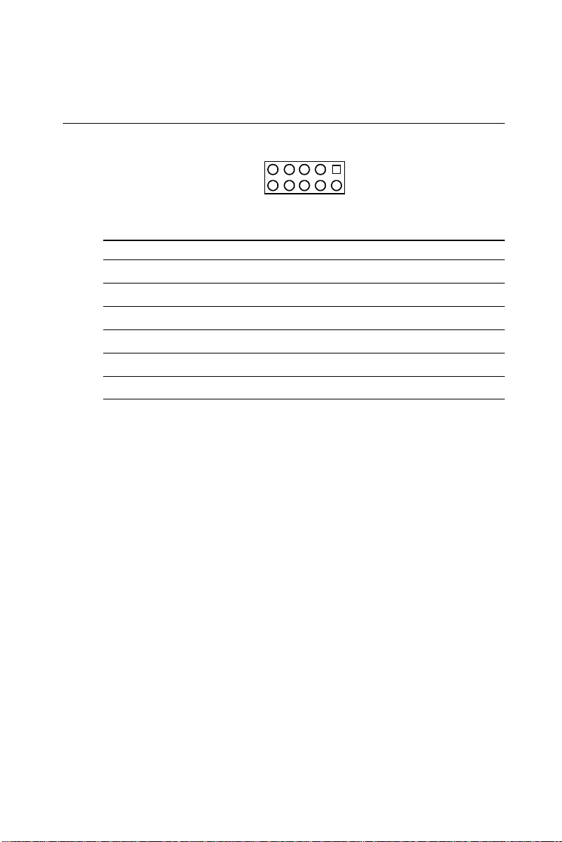
C.14 COM2 RS-232 connector (CN15)
57693
1
10
8
Table C-13: COM2 RS-232 connector (CN15)
2
4
Pin RS-232 port Pin RS-232 port
1 DCD 6 CTS
2 DSR 7 DTR
3 RxD 8 RI
4 RTS 9 GND
5 TxD 10 N/C
Appendix C Pin Assignments 87
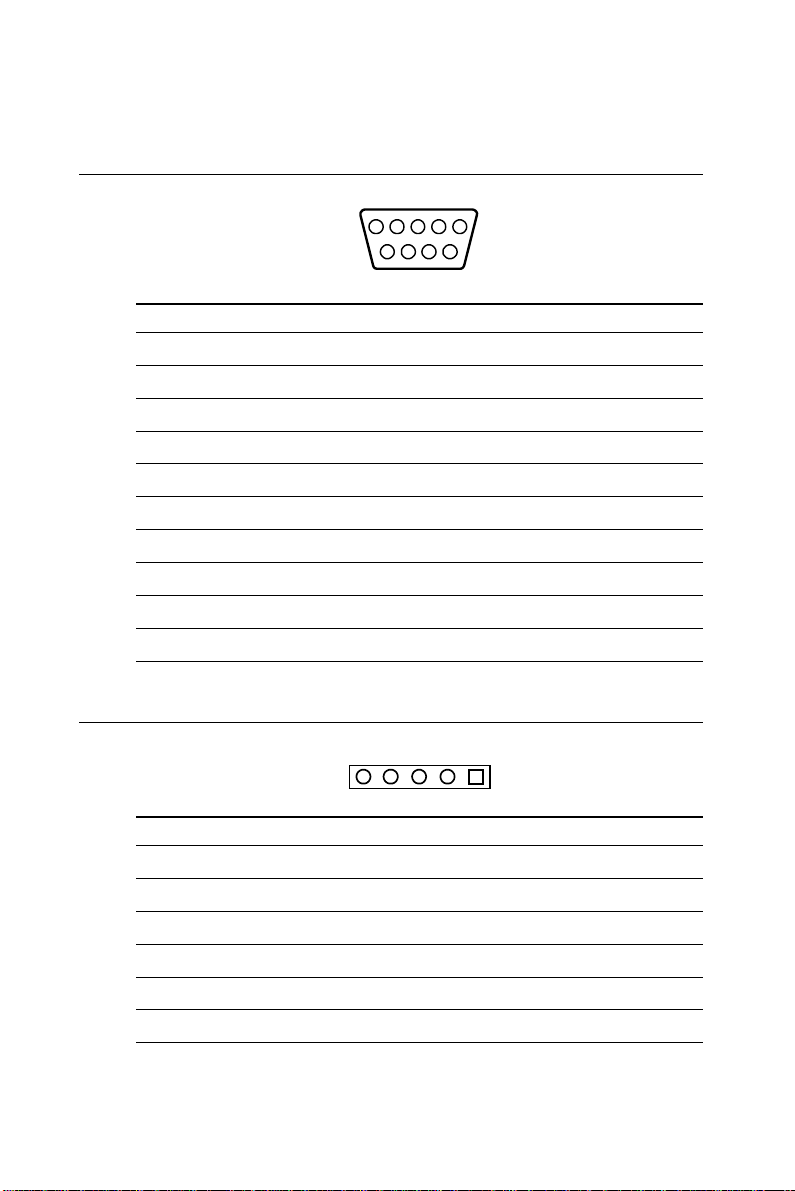
C.15 COM1 RS-232 connector (CN16)
15
324
78
9
6
Table C-14: COM1 RS-232 connector (CN16)
Pin Signal
1 DCD
2 RXD
3 TXD
4DTR
5 GND
6 DSR
7 RTS
8 CTS
9RI
C.16 External keyboard connector (CN17)
54 231
Table C-15: External keyboard connector (CN17)
Pin Signal
1 CLK
2 DATA
3NC
4 GND
5+ 5 V
88 PCA-6751 Series User's Manual

C.17 ATX power connector (CN18)
1
2
3
Table C-16: ATX power connector (CN18)
Pin Signal
1 5 V SB
2 N/C
3 PS_ON
C.18 AT power connector (CN20)
1
2
3
4
Table C-17: AT power connector (CN20)
Pin Signal
1 +12 V
2 GND
3 GND
4 +5 V
Appendix C Pin Assignments 89
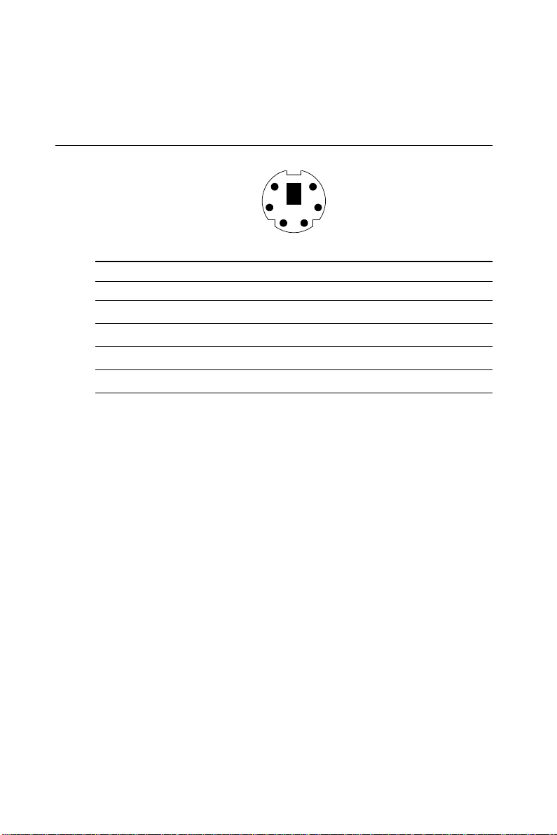
C.19 Keyboard and PS/2 mouse connector
(CN21)
6
4
Table C-18: Keyboard and PS/2 mouse connector (CN21)
Pin Signal
1 KB DATA
2 MS DATA
3 GND
4 +5 V
5
3
12
90 PCA-6751 Series User's Manual

C.20 CompactFlash™ card connector (CN24)
Table C-19: CompactFlash™ card connector (CN24)
Pin Signal Pin Signal
1 GND 2 D03
3 D04 4 D05
5 D06 6 D07
7 *CS0 8 A10
9 *ATA SEL 10 A09
11 A08 12 A07
13 +5 V 14 A06
15 A05 16 A04
17 A03 18 A02
19 A01 20 A00
21 D00 22 D01
23 D02 24 -IOCS16
25 *CD2 26 -CD1
27 D11 28 D12
29 D13 30 D14
31 D15 32 -CS1
33 *VS1 34 -IORD
35 *IOWR 36 -WE
37 INTRQ 38 +5 V
39 *CSEL 40 -VS2
41 *RESER 42 IORDY
43 *INPACK 44 -REG
45 *DASP 46 -PDIAG
47 D08 48 D09
49 D10 50 GND
* low active
Appendix C Pin Assignments 91
 Loading...