

Page 1
Twin Stabilised
D.C. Supplies
PP3& PP3R
Instruction Manual
Page 2
Twin Stabilised
D.C. Supplies
P P3 & PP3R
Instruction Manual
ADVANCE E LECT RONI CS L IM I T ED
INSTRUMENT DIVISION
ROEBUCK ROAD, H A iN AU lT , ILFORD. ESSEX, ENG LAND
TELEPHONE HAIN AULT 4444 TELEGRAPH ATT E N U ATE, ILFORD
Publication I 209
I l*i [PIia! m I ngl.iiKi
1
Page 3
Co ntents
S E C T IO N I In tr o d u ctio n 3
SE C T I O N 2 Spe cific atio n 4
S E C T IO N 3 O per at i n g In stru c t i o ns 5
3.1 Preparations for Use 5
3. 2 Metering 5
3.3 Overload 5
3.4 Four Terminal Network 5
3.5 Fuses 5
S E CT I O N 4 C ir c ui t D e sc rip t io n 6
4.1 General 6
4.2 Stabilising Circuit 6
4.3 Overload Cut-out 6
S E CT I O N 5 M a in t e n a n c e 7
5.1 General 7
5.2 Re-alignment of Voltage Calibration 7
5.3 Adjustment of Overload Cut-out 7
S E CT I O N 6 C o m po n en t s Li s t 9
SE CT I O N 7 Fa c t o ry Se r v i ce 10
Illu stra tio ns
Fig. I Componen t Location Diagram X
Fig. 2 Circuit Diagram 9
2
Page 4

1 1 ntrod uc ti on
Th e T win Stabilised D.C , Su pply PP 3 is a por table
instru ment prov iding two i ndep enden t an d floating
stabilised d.c. supplies, each variabl e from 0 to 30V at
1A m axim um . Th e tw o supplies can be used se parately,
or connec ted in series to pr ovide a max im um o utp ut of
60V at 1A.
In bo th sections of the instru ment, the rang e is covered
in three o verla ppin g no min al 10V steps, wit h fine
adjus tment pr ovided by a variable co ntrol directly
calibrated in volts. A voltm eter and a dual -ran ge
am me ter are pro vided, an d these can be switched
indep endently to m oni tor eith er section.
Both sections are p rovided with f our ter minal o utp ut
netwo rks wh ich virtually elim inate the effect of
resistance in the c onnec ting leads to the load.
Overl oad p rotection is effected by an e lectronic circuit
which affords co mplete protec tion agai nst b oth
progressive a nd sud den short circuit overloa ds. This
circuit is reset from the fro nt panel by o per atio n o f the
o n /o f f switch.
Th e instrum ent will oper ate from a.c. suppli es of 90 to
130V and 200 to 240V. Fuses ar e pro vided to protect
against bot h suppl y surges a nd in ternal c om pon en t
failure. Th e T win Stabilised D.C . Sup ply PP 3R is a
19-inch rack m ou ntin g version of the PP3. Th e specifi
cation is identical to the PP3 but the P P3 R has the
addition al facility o f the ou tp ut being avai lable o n a
10-way ter minal block at the re ar of the instrum ent.
3
Page 5
2 S pec if ica ti on
Po w e r R eq u i r em ents T he in strumen t o perates
from an a.c. sup ply of 90 to 130V, or 200 to 240V, at
40 to 60e/s,
Per f o rm a n c e ( e a ch un it) o u t p u t v o l t A GF. Oto
30V d.c. in three o verlapp ing ranges, 0 to 10V, 10 to
20V an d 20 to 30V.
OUTPUT CURRENT OtolA,
o u t p u t im p e da n ce d .c.— less than 0-01 oh ms,
a.c. ( up to lOOkc/s)—less than 0*2 oh ms.
ri p p le Less t han ImV pe ak-to-pe ak.
st a b i l i s a t i o n Allowable supply variation from n o m i
nal value is j_7°,0 before loss o f stabilisation or
co mpo nent ove rloa ding occurs. Ch ang e o f ou tput
voltages du e to supply i nput var iation o f ± 7% is
app roxim ately lOmV.
M e te r i n g Tw o meters are fitt ed: a n a mm et er which
can be sw itched to either supply, ranges 0 to 1A an d 0
to 0-1A F .S .D .; a voltmeter w hich can be switched
lo read either ou tput voltage with an acc uracy o f
2°/
Vo l t a ge C alib r at i o n Th e c oarse an d line voltage
setting con trols arc calibrated to a n acc uracy o f
ap proxi mate ly 0-2V, using external meters.
O v er l o a d P ro t e cti o n Provid ed by electronic cut
outs which can be reset f rom the front panel.
O p e r a tin g T e m per a tu r e Th e in stru ment can
ope rate at full load in am bient tem pera ture s up to
35 ('. .
Dim e ns i o ns P P 3 W idth I8in., depth 1 U in., height
13jin. (46 x 29 • 34cm).
Dim e n si o n s PP3R W idt h I9in., height 12|in.,
dep th 9£in. b ehind pa nel and I Jin. projecting in front
of panel' (48-25 x 31 x [24 + 3-5]cm).
W e i g h t 381b (17kg).
F i n i sh PP 3 D ark blue metal case with light grey
front panel and me dium grey su rroun d. All co lour s to
B.S.2660. C ase tint N o. 7-0 86, front panel tint No.
9-093, fr ont panel s urr oun d tint No , 9-095.
PP3 R Panel an d pro tectio n cover d ark a dmi ralt y grey
to B.S.381.C, tint No . 632.
Page 6
3 O p e ratin g In stru ctio ns
W a rnin g ,
This i nstr ume nt uses transistors, and for this reason it
should not be opera ted in am bient t empe rature s in
excess o f3 5° C (95 F), or un der condit ions which limit
free circulation of air throu gh the ventilation panels.
3.1 P r e p a r a t i o n s f o r u s e
Re move the rec tangula r plate that covers the a.c.
supply soc ket at the rear o f the case, a nd e nsure that
the supp ly voltage adjustm ent panel is correctly set for
the local supply, and that the correct fuse is fitted.
Alternativ e fuses are provided, a 3A fuse for use when
the in strum ent is op erated f rom a 200 to 240V supply,
and a 5A fuse for ope ration fro m a 90 to 130V supply.
Th e fuse not in use is carried in a clip next to the supply
socket. Switch the am mete r selector switch to on e of
the 1A ranges, and c onnect the load or loads to the
o u t p u t terminals. Th e two sec tions of the inst rument
can be con nected in series if mo re t han 30V is required,
but under no circ umstanc es shou ld the tw o sections be
connec ted in parallel.
Con nect the inst rument to the a.c. supply, set the
out put voltage c ontrols to the require d setting, and
switch
o n . .
3.2 M e t e ri n g
The a mm ete r and vo ltmeter can be switched inde pen
dently to mo nitor each section o f the instru ment. W hen
the two supplies are used in series, the ou tput voltage
is indicated by the su m of the two voltme ter readings,
3.3 O v e r l o ad
The o verload circuit will oper ate whe n the load current
exceeds ap proxi matel y 1-4A. To reset, switch the
supply switch to of f , wait three se conds, a nd then
switch o n again.
It should be noted that the conn ectio n o f a capacitive
load to the out put terminals, while the ins trumen t is
opera ting, can cause the cut-out to op erate due to the
initial surge current.
3.4 F our T e r m i n a l N e twor k
The fou r terminal n etwor k is pr ovide d to ke ep the
voltage acro ss the load cons tant irrespective of voltage
dr op occ urring alo ng the d.c. supply leads.
To m ake use o f this facility, use two furt her leads of
any conv enient g auge to co nnect each end o f the
actual load to the app rop riat e p o te n ti a l terminals.
3 . 5 Fuses
The a.c. input circuit includes a single fuse, the rating
of which is chosen ac cord ing to the s upply voltage. In
the lower voltage range, 90 to 130V, the fuse rating is
5A, for the higher voltage range, 200 to 240V, the fuse
rating is 3A.
The internal circuits are pr otected by two 3.A fuses.
Page 7
4 Ci rcui t Des cr i ption
4.1 G e n e r a l
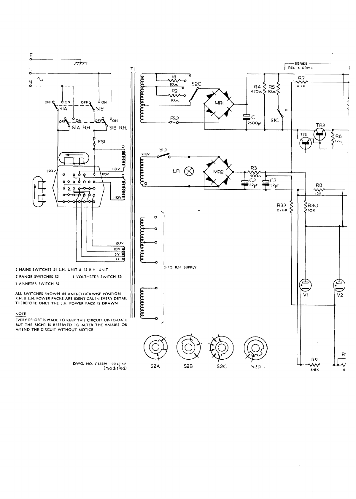
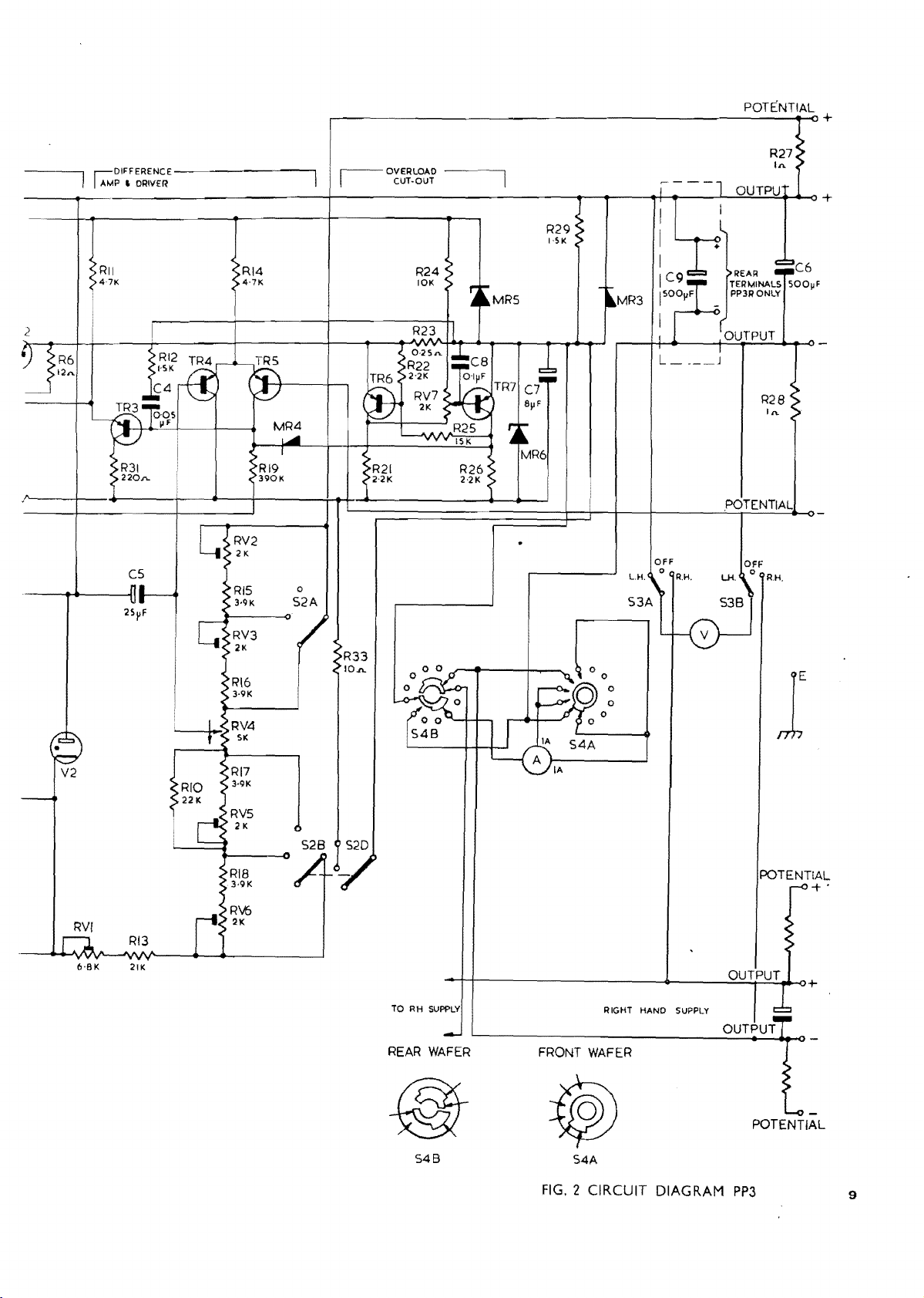
The two sections o f the PP3 ; ii t identical, and the
circuit di agram in fig . . show s only on e section
complete.
The a.c. input is app lied to the t r a nsf or m e r (TIS
primary win ding via sections A and B o f th e on- ' o i i
switch, the fuse FSI and the s u ppl y voltage tapping
panel. Th e su pply trans form er has one high vo l ta g e
and one low voltage s e c o n d a ry windin g for each
sec tio n , the low voltage w ild ing being lappe d to
provide three ou tpu t \o ltr gc ranges. T o prevent
switching surges, resistors R1 am! R2 are switched into
eireuil m omen tarily as th e ra nee s w i tc h is o perated,
A selenium bridge rectifier, M R I, rectifies the out put
from the low- voltaec winding, an d the resulting d.c. is
smo othed by the 2500;*F capac itor Cl an d fed to the
outp ut terminals via the series regu lator transistor
TR2. O r e section o f the c urrent switch S4, inserted in
(lie line to the negative out put terminal , is used to
snitc h the internal a mm ete r into circuit wh en required.
The voltmeter isco nne ctcd acro ss the ou tpu t terminals
by mea ns o f switches S3 A a nd S3H.
A bleed resistor R4 is perm anen tly c onnec ted across
Cl , the Mi ioothmg capacitor , and this is paralleled b\ a
lOohm resistor R5 whe n the unit is switch,ed of!'. R2()
is a further bleed resistor connecte d across C6 and any
capacity in the load circuit to provi de a discharge
path in dependent o f the scries re gulato r T R2.
4.2 Sta bi l is in g C ir cu it
The o utpu t from the high \olt age secon dary winding
of Tl is rectified by the selenium bridge rectifier M R2.
sm ooth ed by an R C filter C2. R3 and 0 3, an d used to
provide a reference \ol tage \ la two ca scaded neon
stabilisers VI (150V) a nd V2 (85V).
A potential divider netwo rk, R V2 to R V I , is con nected
across the neon stabiliser V2, via the lo hm resistoi
R27. Th e voltage at the wi per o f RV4, the front panel
\olta ge control, is c omp are d with the p otential across
the o utpu t terminals by m eans of a differential
amplifier, the long-tailed pair T R4 and T R5. Sections
A and B o f switch S2 adjust the potential divider ratios
as each o utp ut voltage range is selected. T he preset
contro ls in the divid er netwo rk are incl uded to p er mit
ac c u ra t e c alibratio n of the voltage ranges.
Any o utpu t from the differential amplifie r is curre nt-
amplified by two emit ter follower stages TR 3 and TR I,
and appli ed as a corre ction signal to the base o f the
series regula tor TR 2. T he effective imp eda nce o f T R2
is thus ad justed until the out put an d reference voltages
a re‘equal.
A fo ur-term inal o ut p u t net work is provi ded, an d when
this is in use the po te n t i al term inals are conn ectcd
indep endent ly t o the load. T he stabilising circuit thu s
cont rols the actu al voltage across the load, virtually
elimina ting the effect of the resistance o f the pow er
suppl y leads. •
The correct ope ratin g potentials for the t ransisto r
circuits, includin g the over load cut-out, are derived
from the high voltage d.c. supp ly via the zene r diodes
M R5 and MR6 .
4.3 O ver l o a d C u t -o u t
Tran sistor s T R 6 and T R 7 const itute a bi-stable
mult ivibra tor circuit with T R6 norm ally con ducting .
Wh en the o utp ut curr ent fr om th e section exceeds a
pred etermin ed val ue , the potential dev eloped across
the series resistor R23 triggers the mu ltivib rator which
then ch a ng e s its slate. T R7 n ow c ond ucts and the
potential d eveloped acro ss R 26 is used to sh u t -ol T the
dilleienlial amplifier, caus ing the section o utp ut
voltage to fa l l to zero. T he ge rm aniu m d iode M R4
is includ ed in circuit to block signals f rom the diller-
eimal amplifier w hich might' o therwis e trigger the
muliivi brator.
To reset the c ut-out c ir cui t it is only necessa ry to
switch the u ni t o h - f o r a lew- s ec on d s, a nd th en switch
on again. T he mul tivib rato r w il l then be in its original
slate w i t h TR 6 co nduc t i ng.
The selenium rectificr M R 3 is conn ected acr oss the
out put termi nals to prevent the de velo pm ent of a
reverse voltage w hen the cut-o ut op erates . This
provision is parti cularly necessary when the two supply
sections are o pera ted in series.
Page 8
5 M a in te n a n c e
5.1 G e n e ra l
The PP3 is of robu st co nstruct ion, an d em ploy s semi
cond ucto rs th rou gho ut, with the exceptio n of the two
neon stabilisers. A high level o f reliability has been
achieved and the instru ment sh ould op era te indefinitely
withou t requiring extensive m ainten ance . In cases of
difficulty, it is re com me nd ed that the in strum ent is
returned to the factory for atten tion.
To o btain access to the internal co mpo nen ts, place the
instrument face dow nw ar ds on a Hat surface, remov e
the four retaining screws in the back, and lift off the
case. Fin. / show s the location of the co mp one nts on
the chassis assemb ly.
To rem ove the con trol kn obs, it is lirsi necessary to
remove the sp ring-loade d plastic section o f each kn ob
to expose the retain ing screw. W he n replacing the k nob
ensure that the inden tation o n the top of the plastic
section coincides with the curs or on I he skirt.
Voltage cal ibration accurac y using the built-in volt
meter is 2 Increased accura cy c an be ob tain ed b\
using a suitable external m eter co nnec ted direetlv
across tiie voltm eter terminals.
5.2 R e-alig n m e n t o f V olta ge C a l i b ratio n
To re-align I he v oltage calibra tion using internal or
exterra I meters, pr oceed as follows: -
I. Remo ve the inst rumeni from the case, connec t it
to the a.c. supply, and switch on.
3. Set the vol tmeter selector '-witch to the required
seci ion.
3. Sei the range selector switch to the 0 ION'
position, a nd adjust [he variab le c ontro l to give a
leading of exactly IV on the voltmete r.
4. Check that the cu rsor on the variable co mroi
indicates 'I '. If necessaiv, rota te the co ntrol kno b
on its spindle until the ali gnment is correct.
5. Switch to the 20 30V rar-gc and .set the variable
conti ol to ’10'. Adjust R \ I, located near the
valves on the main ch assis, until the vollmetci
indicates exaetls 30 V (a ccuracy • 2 i.e. 0-6V
using internal meter).
(' Set the variable control lo ‘O ' a ml adjust RV2
(sec/a*. I) with an insulated rod until the vollmelet
indicates exactlv 20V.
7. Repeat 5 a nd 6 until no I'ui liter adj ustm ent is
necessary.
8. Svvitch to the 10- 20V range, set the variable
control to ‘10’ an d adjust R V5 until the m eter
indicates 20V (accurac y : 2 ,\„ i.e. : 0-4V using
internal meter).
9. Set the variable control to ‘O' and adjust R V 3 until
the meter indicates 10V (accur acy : 2 <>0 i.e. ; 0-2V
using internal meter).
10. Rep eat 8 and 9 until no f urther a djus tmen t is
necessary.
I I. Switch to the 0- 10V range, sei the variable control
to '10' and adjust RV 6 until the m eter indicates
10V. T he voltage c alibratio n shou ld no w be
correct.
5.3 Adju s t m en t o f O v er l o a d C ut-o ut
To adjust the over load cut- out, a multi meter such as
the Avo metc r mod el 7 o r 8 an d a variable resistor
rated at 0 to 10 o hms (m inim um ) I -5A , will be
required. To m ake the ad justm ent, pro ceed as
fol lows:
1. R emov e the ins trume nt from the case, and invert
the chassis.
2. Set the slider o f the a ppr opr iate section p otent io
meter R V7 (located at the front o f llie c o m p o nent
boa ri l l to that end o f the pot entio meter track
connec ted lo the I0K resistor.
3. Set the m ultime ter to the I0A range and connec t
it in series with the load resistor a cross the outp ut
terminals of the supply. Set the oa d to m axi mum
resistance and switch off the internal a mmeter .
4. Set the ou tput to NY and switch on
5 Adjust the load resistoi until the mult imeter
indicates a current of I -4A.
ft. Move the slider o f RV ~ a wav from the INK
resistoi- end of its track until the outp ut drop s
siiddenlv to zero
~. Switch oil, slightly iiieieasc die load resistance
and then switch o \ again.
N. Decrease the lo ad resistance an d cheek t h a t the
cut-out again op er a te s at 1-4A. If the cut -out fails
to o p e r a te at th e c o rr ec t level, r e- a dj u st RV7 as
iiecessarv.
Page 9
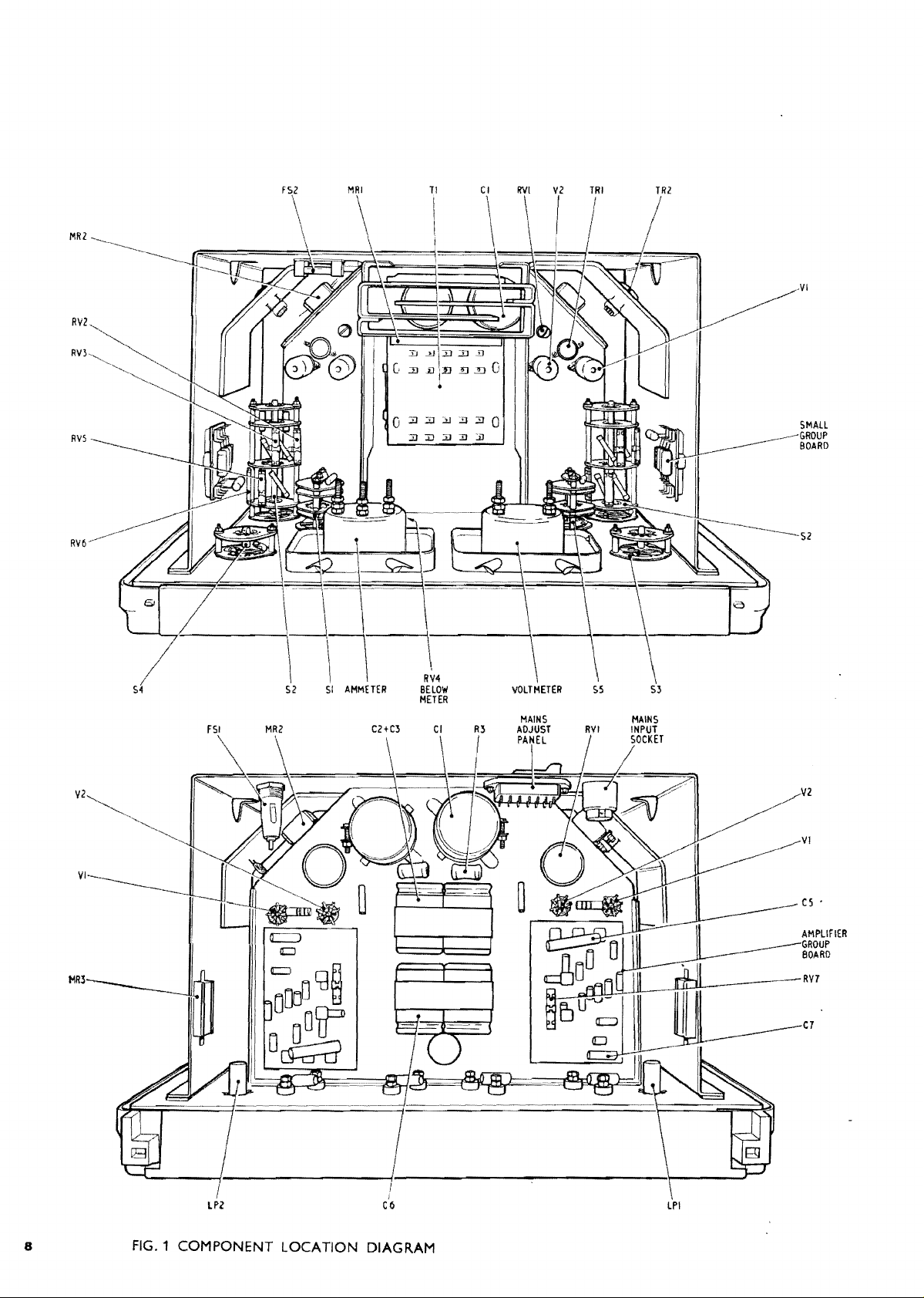
FS1 MR2 C2 + C3 Cl RJ ADJUST RVI INPUT
MAINS MAINS
8
FIG. 1 C O M P O N ENT LO C A TIO N DIAG R AM
Page 10
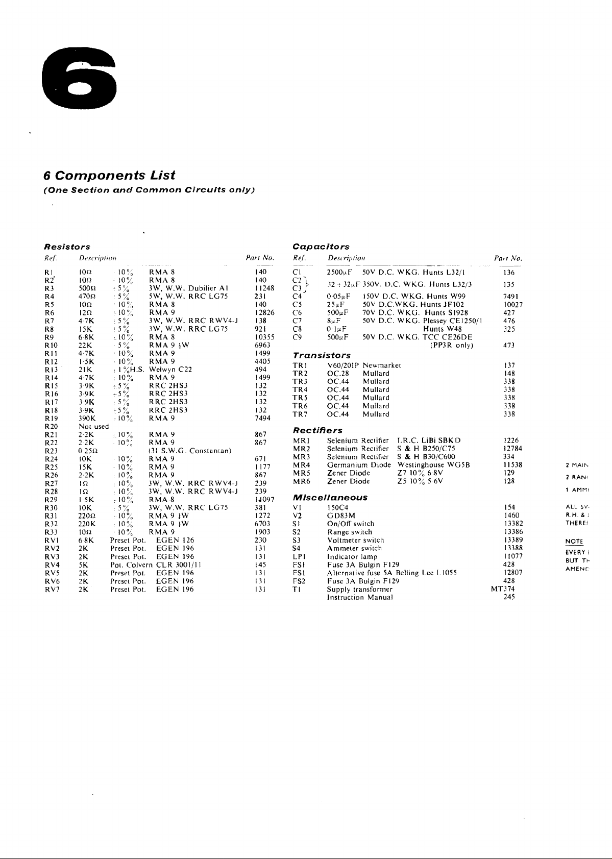
6 Com p onents List
(O n e S ec t io n a n d C o m m on C i rc uits o n l y )
R esi st ors C ap a citors
Kef.
RI
R2‘
R3
R4
R5
R6 I 2n
R7
R8
R9
RIO 22K
RI I
Rl 2
RI3
R14
R 15
R16
RI7
RI8
R 19
R20
R21
R22 2 2K
R23 0 -2 5n
R24 I0K
R25
R26 2 2K
R27 in
R28
R29 I-5K
R30
R31
R32 220 K
R33
RVI 68 K
RV2
RV3 2K Preset Pot.
RV4
RV5 2K Preset Pot.
RV6 2K
RV7
Description
io n
io n
SOOn
470 0
io n
4 7K
15K
6-8K
4-7K
1 5K
21K
4 7K
3-9K
3-9 K.
3 9K
3 9K
390K
Not usee
2-2K
I5K
in
10K
220n
ion
2K Preset Pot. E G E N 196 131 S4
5K Pol. Colve rn C L R 3001/11
2K
■ 10%
; 10%
; 5 %
! 5 %
' 10%
:-10%
: 5 %
! 5%
l !0% RM A 8 10355
■ 5%
‘ 10%
-1 0 %
: 1 %H. S.
: 10%
"I" 5 /o
r 5 %
• 5 %
--5%
: 10%
10 % R M A 9
10%
- 10%
- 10 %
: 10%
: 10%
: 10%
r 10%
- 5 %
r 10%
: 10%
: 10%,
Preset Pot.
Preset Pot. E G E N 196
Preset Pot. E G E N 196 131 T1
RM A 8
RM A 8
3W, W.W , Du bilie r Al
5W, W . W . RRC L G 75
RM A 8
RM A 9 12826
3W, W. W . RR C R WV 4-J
3W, W.W . R R C LG7 5
RM A 9 1W
RM A 9 1499
RM A 9
Welwyn C22
RMA 9
R R C 2H S 3
RR C 2 HS 3
RR C 2HS 3
RR C 2HS 3
RMA 9
RM A 9
(3! S .W . G . Co n s ta m a n )
RM A 9
RM A 9
RM A 9 867
3W, W.W . RR C
3W, W.W . R R C
RM A 8
3W, W .W . R R C
RM A 9 JW
RM A 9 JW 6703
RM A 9
EGEN 126
EG E N 196
EG E N 196 131
RWV 4-J 239
RWV 4-J
LG75
Pari N o,
140
140
11248
231
140
138 C l
921
6963
4405
494
1499
132
132
132
132
7494
867
867
671
1 177
239
IJ097
381
1272
1903
230
131 LPI Ind ica to r la mp
145
131
Ref,
Cl 2500sxF 50V D.C. WK G . H u nt s L32/1
C 2 \
C3 /
C4 0-05 nF 150V D .C. W K G . H u nt s W99
C5 2 5n F 50V D .C . WK G . Hu n ts J F I0 2
C6
C8
C9
Description Pari No.
32 I 32u F 350V. D.C. W K G . H u nt s L32/3
500 nF 70V D .C. W K G . Hu nt s S1928
8m-F 50V D .C. W K G . Plessey C E 1250/1
0- l n F Hu nt s W48 325
500 nF 50V D .C. W K G . TC C CE 2 6 D E
T ra n s is t ors
TR I
TR 2
TR 3
TR 4
TR 5
TR 6
TR 7
V60/2QIP New m ark et
OC. 28 Mul lard
OC. 44 Mul lard
OC .4 4 Mulla rd
OC .4 4 Mulla rd
OC .4 4 M ullard
OC .4 4 Mu llard
Re ctifi e r s
MR1
MR 2
MR 3
MR 4 Ge rm a n i u m Dio de W es tin gho use WG 5 B
MR 5
M R6 Zen e r Dio de Z5 10 % 5 6V
Selen ium Rectifier I.R .C . LiBi S B K D
Selen ium Rectifier S & H B250/C75
Selen ium Rectifier S & H B30/C600 334
Zen er D io de Z7 1 0% 6 8V
M i s cell a n eo u s
VI
V2
SI
S2 Rang e switch
S3
FSI
FS1
FS2
150C4
GD 8 3 M
On /O f f switch
Volt me ter switch
Am m e te r switch
Fuse 3A Bulgin F I29
Altern ati ve fuse 5A Belling Lee LI055
Fuse 3A Bulgin F129
Sup pl y t ra nsf or me r MT374
Instr uct ion Man ual 245
(PP 3R only)
136
135
7491
10027
427
476
473
137
148
338
338
338
338
338
1226
12784
11538
129
128
154
1460
1 3382
13386
13389
13388
11077
428
12807
428
2 MAIN
2 RAN!
1 AMMt
ALL SV-
R.H. 8, :
THERE?
NOTE
EVERY I
BUT Tb
AM ENT
Page 11
E
o
L
I
--------
SERIES —
I Reg. « d riv e
2 MAINS SWITCHES St L.H. U NIT & S5 R.H. UNIT
2 RANGE SWITCHES S2 1 VOLTMETER SW ITCH S3
1 AMMETER SW ITC H S*
ALL SWITCHES SH O W N IN AN TI-CLOC K W ISE PO SITION
R.H. & L.H. POWER PACKS ARE IDEN TIC AL IN EVERY DETAIL
THEREFORE O N LY THE L.H. POWER PACK IS DRA W N
NOTE
EVERY EFFORT IS MADE TO KEEP THIS CIRC U IT UP-TO-D ATE
BUT THE RIGHT IS RESERVED TO ALTER THE VALUES OR
AMEND THE C IRCUIT W IT HO UT NOTICE
DW G . NO. C13529 ISSUE 17
(m o d i f ie d )
Page 12
potential
FIG, 2 CIRCU IT DIA GRA M PP3
Page 13
7 F a cto ry S erv ice
Our Factory Service Department is at your disposal should
you wish to obtain further repair information by telephone
or letter. The Type and Serial N umbe r of the instrument
should always be quoted. We maintain an efficient service
facility and the instrument can, if necessary, be returned to
our factory for repair.
The instrument is guaranteed for a period of one year from
its delivery to the purchaser for the replacement of defective
parts, other than valves, semiconductors a nd fuses.
Valves and semiconductors are subject to the manufac
turer’s guarantee.
Full details of the service or repair required should accom
pany equipment returned to us for servicing. The equipment
must be adequately packed, preferably in the special box
supplied, and shipped with transportation charges pre
paid. We can accept no responsibility for instruments
arriving damaged. Should the cause of failure during the
guarantee period be due to misuse or abuse of the instru
ment, or if the guarantee has expired, the repair will be
charged and put in hand without delay unless other instruc
tions are received.
OUR SA LES, SERVICE AND EN GIN EE R ING DEPAR T MENTS ARE AT
YOUR SERV ICE AT A LL TIMES.
Manual Part No. 245
 Loading...