

Advanced Power Technology APT ARF461B, ARF461A Datasheet
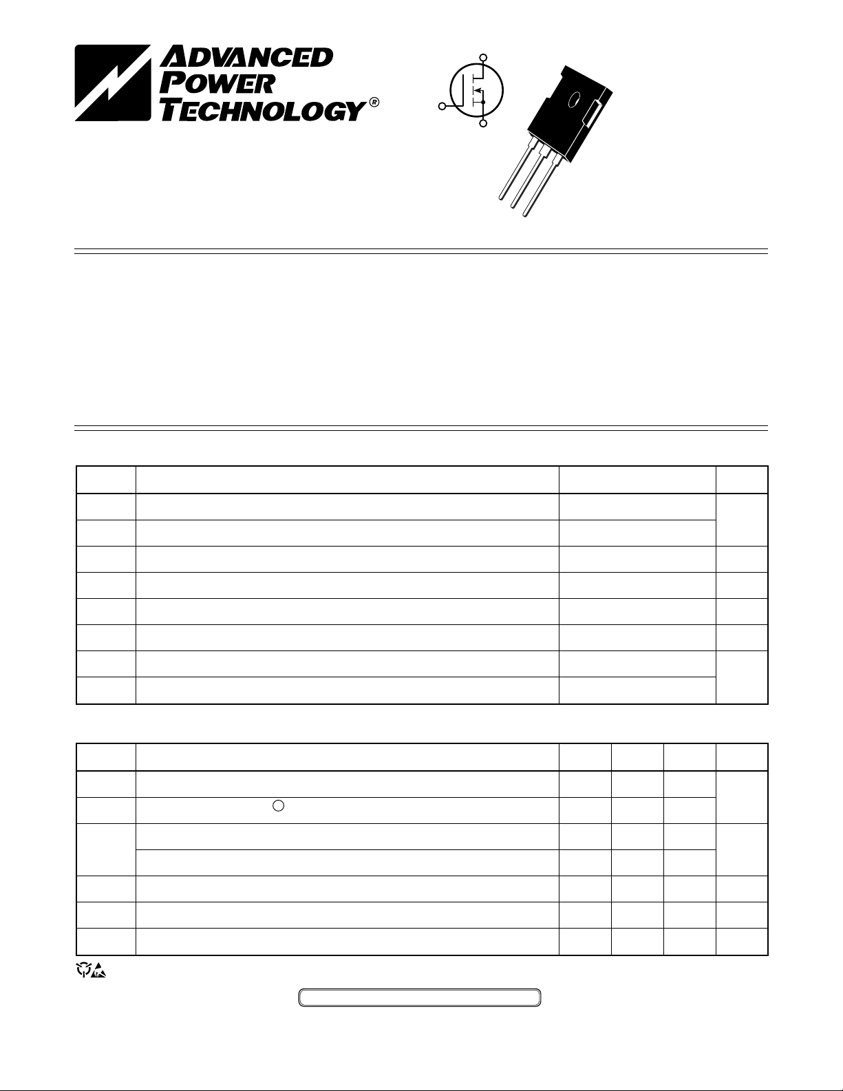
D
ARF461A
G
S
TO-247
ARF461B
Common
Source
RF POWER MOSFETs
N-CH ANNEL ENHANCEMENT MODE 250V 150W 65MHz
The ARF461A and ARF461B comprise a symmetric pair of common source RF power transistors designed for pushpull scientific, commercial, medical and industrial RF power amplifier applications up to 65 MHz. They have been
optimized for both linear and high efficiency classes of operation.
• Specified 250 Volt, 40.68 MHz Characteristics:
• Output Power = 150 Watts.
• Gain = 13dB (Class AB)
• Efficiency = 75% (Class C)
MAXIMUM RATINGS All Ratings: TC = 25°C unless otherwise specified.
Symbol
Parameter
• Low Cost Common Source RF Package.
• Low Vth thermal coefficient.
• Low Thermal Resistance.
• Optimized SOA for Superior Ruggedness.
ARF461A/B
UNIT
V
V
V
R
TJ,T
DSS
DGO
I
P
qJC
T
Drain-Source Voltage
Drain-Gate Voltage
Continuous Drain Current @ TC = 25°C
D
Gate-Source Voltage
GS
Total Power Dissipation @ TC = 25°C
D
Junction to Case
Operating and Storage Junction Temperature Range
STG
L
PRELIMINARY
Lead Temperature: 0.063" from Case for 10 Sec.
STATIC ELECTRICAL CHARACTERISTICS
Symbol
BV
VDS(ON)
I
DSS
I
GSS
g
VGS(TH)
Characteristic / Test Conditions
Drain-Source Breakdown Voltage (V
DSS
On State Drain Voltage
Zero Gate Voltage Drain Current (V
Zero Gate Voltage Drain Current (V
Gate-Source Leakage Current (VGS = ±30V, V
Forward Transconductance (VDS = 25V, ID = 3.25A)
fs
Gate Threshold Voltage (V
1
(ID(ON) = 3.25A, VGS = 10V)
DS
DS
= VGS, ID = 50mA)
DS
= 0V, ID = 250 µA)
GS
= V
= 0.8 V
, VGS = 0V)
DSS
, VGS = 0V, TC = 125°C)
DSS
= 0V)
DS
1000
1000
Volts
6.5
±30
250
0.50
Amps
Volts
Watts
°C/W
-55 to 150
300
°C
MIN TYP MAX
UNIT
1000
6.5
Volts
25
250
µA
±100
34
35
nA
mhos
Volts
CAUTION: These Devices are Sensitive to Electrostatic Discharge. Proper Handling Procedures Should Be Followed.
APT Website - http://www.advancedpower.com
USA 405 S.W. Columbia Street Bend, Oregon 97702-1035 Phone: (541) 382-8028 FAX: (541) 388-0364
EUROPE Chemin de Magret F-33700 Merignac - France Phone: (33) 5 57 92 15 15 FAX: (33 ) 5 56 47 97 61
050-5987 Rev A 7-2001
DYNAMIC CHARACTERISTICS ARF461A/B
Symbol
C
iss
C
oss
C
rss
t
d(on)
t
r
t
d(off)
t
f
Characteristic
Input Capacitance
Output Capacitance
Reverse Transfer Capacitance
Turn-on Delay Time
Rise Time
Turn-off Delay Time
Fall Time
Test Conditions
V
= 0V
GS
VDS = 50V
f = 1 MHz
VGS = 15V
VDD = 0.5 V
ID = I
D[Cont.]
@ 25°C
RG = 1.6W
DSS
FUNCTIONAL CHARACTERISTICS
Symbol
G
PS
h
y
1
Pulse Test: Pulse width < 380 µS, Duty Cycle < 2%
APT Reserves the right to change, without notice, the specifications and information contained herein.
Characteristic
Common Source Amplifier Power Gain
Drain Efficiency
Electrical Ruggedness VSWR 10:1
Test Conditions
f = 40.68 MHz
= 0V VDD = 250V
V
GS
= 150W
P
out
MIN TYP MAX
UNIT
1700
175
pF
50
8
5
ns
21
10.1
MIN TYP MAX
13 15
70 75
UNIT
dB
%
No Degradation in Output Power
30
25
20
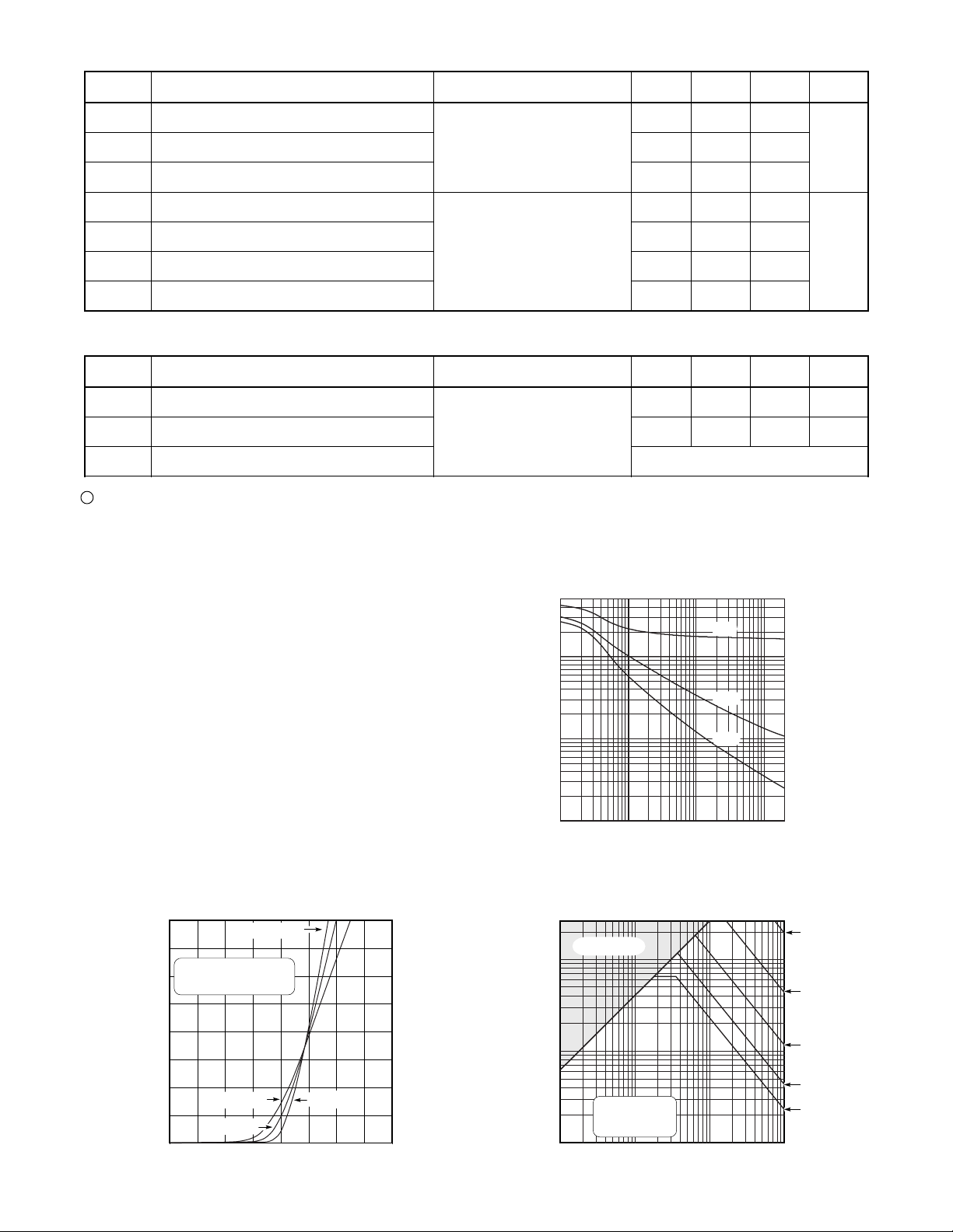
15
GAIN (dB)
10
PRELIMINARY
5
0
30 45 60 75 90 105 120
8
VDS> ID (ON) x RDS (ON)MAX.
6
4
FREQUENCY (MHz)
Figure 1, Typical Gain vs Frequency
TJ = -55°C
250µSEC. PULSE TEST
@ <0.5 % DUTY CYCLE
Class C
V
DD
P
out
= 150V
= 150W
5000
C
iss
1000
500
100
CAPACITANCE (pf)
50
10
.1 .5 1 5 10 50 200
VDS, DRAIN-TO-SOURCE VOLTAGE (VOLTS)
Figure 2, Typical Capacitance vs. Drain-to-Source Voltage
26
OPERATION HERE
LIMITED BY RDS (ON)
10
5
1
C
oss
C
rss
100uS
1mS
10mS
2
, DRAIN CURRENT (AMPERES)
D
I
0
050-5987 Rev A 7-2001
TJ = +125°C
TJ = +25°C
02468
, GATE-TO-SOURCE VOLTAGE (VOLTS)
V
GS
Figure 3, Typical Transfer Characteristics
TJ = -55°C
.5
, DRAIN CURRENT (AMPERES)
D
I
.1
Figure 4, Typical Maximum Safe Operating Area
TC =+25°C
TJ =+150°C
SINGLE PULSE
1 10 100 1000
VDS, DRAIN-TO-SOURCE VOLTAGE (VOLTS)
100mS
DC
 Loading...