

Advanced Power Technology APT ARF441, ARF440 Datasheet
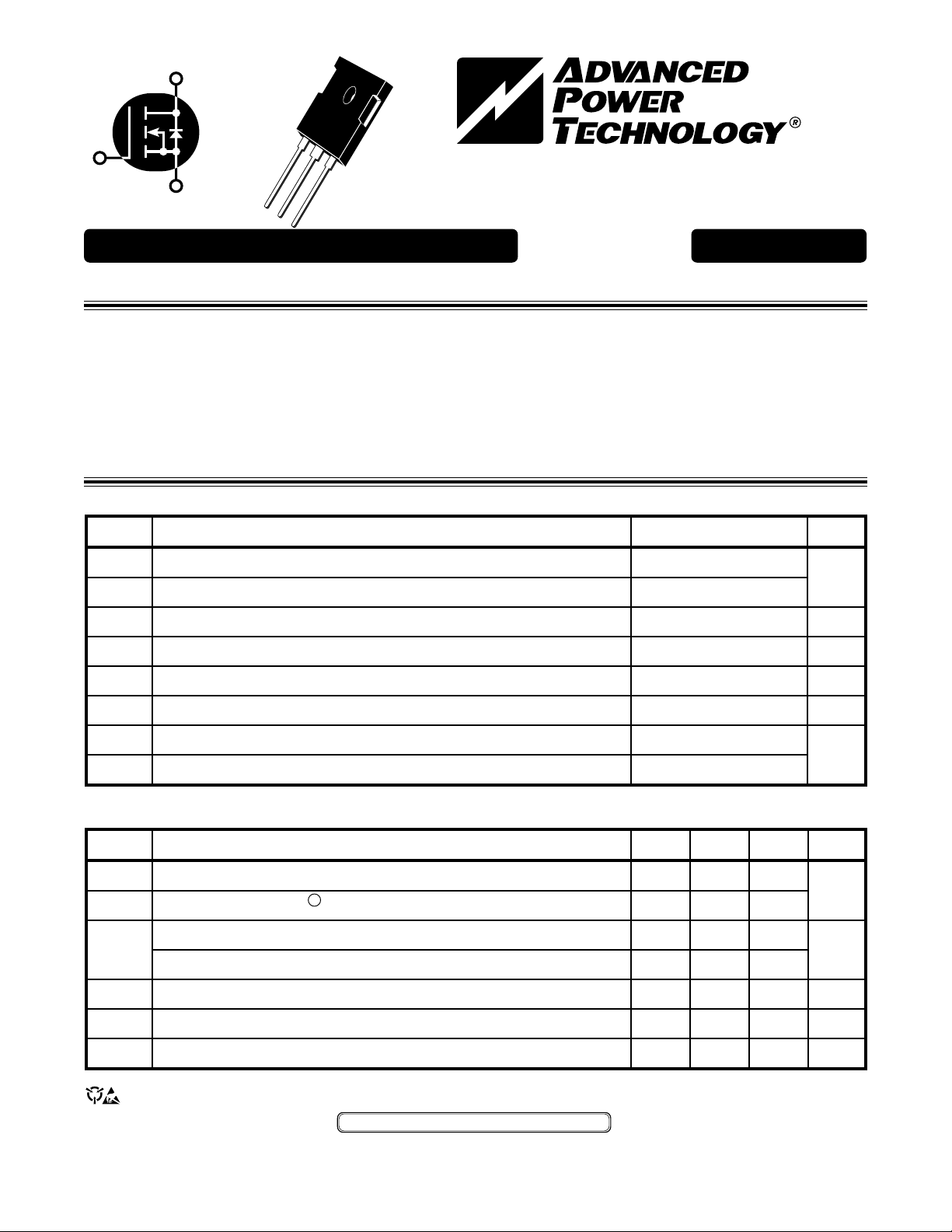
D
G
TO-247
ARF440 125W 50V 13.56MHz
S
RF OPERATION 1-15MHz
()
N-CH ANNEL ENHANCEMENT MODE RF POWER MOSFET
The ARF440 and ARF441 comprise a symmetric pair of RF power transistors designed for narrow-band push-pull
commercial, medical and industrial RF power amplifier applications.
• Specified 50 Volt, 13.56 MHz Characteristics:
• Output Power = 125 Watts.
• Gain = 21dB (Typ.)
• Efficiency = 63% (Typ.)
MAXIMUM RATINGS All Ratings: TC = 25°C unless otherwise specified.
Symbol
V
DSS
V
DGO
I
V
P
R
TJ,T
T
Parameter
Drain-Source Voltage
Drain-Gate Voltage
Continuous Drain Current @ T
D
Gate-Source Voltage
GS
Total Power Dissipation @ TC = 25°C
D
Junction to Case
θJC
Operating and Storage Junction Temperature Range
STG
Lead Temperature: 0.063" from Case for 10 Sec.
L
= 25°C
C
ARF441 125W 50V 13.56MHz
THE ARF440 PIN-OUTS ARE MIRROR IMAGE OF THE ARF441.
POWER MOS IV
• Low Cost Common Source RF Package.
• Very High Breakdown for Improved Ruggedness.
• Low Thermal Resistance.
• Nitride Passivated Die for Improved Reliability.
ARF440/441
150
150
11
±30
167
0.75
-55 to 150
300
®
UNIT
Volts
Amps
Volts
Watts
°C/W
°C
STATIC ELECTRICAL CHARACTERISTICS
Symbol
BV
VDS(ON)
I
DSS
I
GSS
g
VGS(TH)
USA
405 S.W. Columbia Street Bend, Oregon 97702-1035 Phone: (541) 382-8028 FAX: (541) 388-0364
EUROPE
Avenue J.F. Kennedy Bât B4 Parc Cadéra Nord F-33700 Merignac - France Phone: (33)557 92 1515 FAX: (33) 5 56 47 97 61
Characteristic / Test Conditions
Drain-Source Breakdown Voltage (V
DSS
On State Drain Voltage
Zero Gate Voltage Drain Current (V
Zero Gate Voltage Drain Current (V
Gate-Source Leakage Current (V
Forward Transconductance (VDS = 10V, ID = 5.5A)
fs
Gate Threshold Voltage (V
CAUTION: These Devices are Sensitive to Electrostatic Discharge. Proper Handling Procedures Should Be Followed.
1
(ID(ON) = 10A, VGS = 10V)
= VGS, ID = 200mA)
DS
APT Website - http://www.advancedpower.com
= 0V, ID = 250 µA)
GS
= V
DS
DSS
= 0.8 V
DS
= ±30V, V
GS
, VGS = 0V)
, VGS = 0V, TC = 125°C)
DSS
= 0V)
DS
MIN TYP MAX
150
250
1000
±100
45
25
UNIT
Volts
6
µA
nA
mhos
Volts
050-4406 Rev C
DYNAMIC CHARACTERISTICS
ARF440/441
Symbol
C
C
C
Characteristic
Input Capacitance
iss
Output Capacitance
oss
Reverse Transfer Capacitance
rss
Test Conditions
V
= 0V
GS
VDS = 50V
f = 1 MHz
FUNCTIONAL CHARACTERISTICS
Symbol
G
1
Pulse Test: Pulse width < 380 µS, Duty Cycle < 2%
APT Reserves the right to change, without notice, the specifications and information contained herein.
Characteristic
Common Source Amplifier Power Gain
PS
η
Drain Efficiency
ψ
Electrical Ruggedness VSWR 30:1
Test Conditions
= 50V
V
DD
P
= 125W
out
IDQ = 200mA
f = 13.56MHz
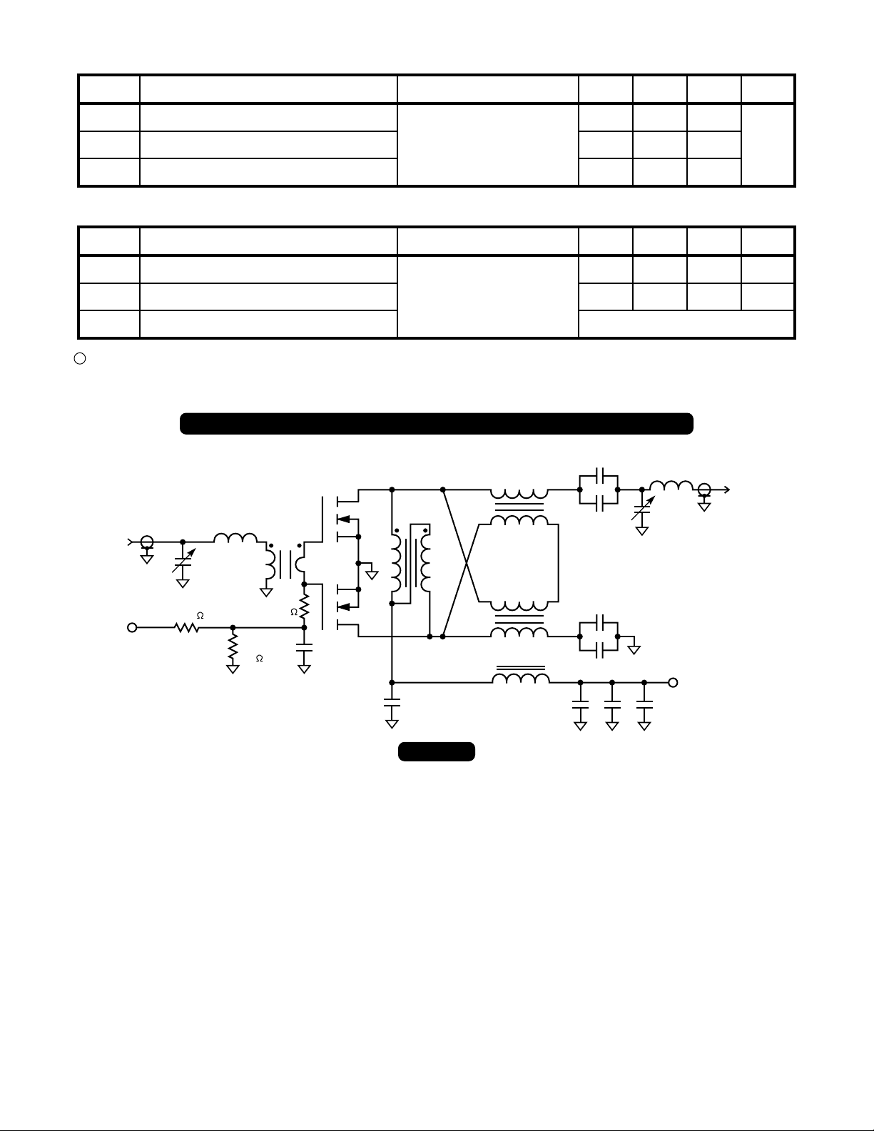
TYPICAL 13.56 MHz, 250 WATT PUSH-PULL POWER AMPLIFIER CIRCUIT
T2
RF
Input
C1
L1
75-480pF
0.5µH
2:1
Q1
T1
BFC1
MIN TYP MAX
UNIT
755 900
155 215
pF
55 90
MIN TYP MAX
18 21
63
UNIT
dB
%
No Degradation in Output Power
ATC"B"
.01µF
C5
C6
.01µF
ATC"B"
C4
L2
25-240pF
0.4µH
RF
Output
ATC"B"
.01µF
C7
C8
.01µF
ATC"B"
C9 C10 C11
.01µF .1µF 10µF (50V)
+
V
I
DD
dq
= 50V
= 0.4A
+Vbias
R3
3.3K
3.3K
Q2
C2
.1µF
C3
.1µF
T3
RFC1
3.3K
R1
R2
Parts List
C1 = 75-480pF Compression Mica
C2, C3 & C10 = .1µF @ 50V, Novacap #1210B104K500N
C4 = 25-240pF Compression Mica
C5, C6, C7, C8 & C9 = .01µF @ 50V, Novacap #1210B103K500N
C11 = 10µF @ 50V Electrolytic
R1, R2 & R3 = 1KΩ, 5%, 1/4W, Carbon
Q1 = ARF440
Q2 = ARF441
L1 = 7.5 T of #18AWG, ID = .438", L = 0.5µH
L2 = 6.5 T of #18AWG, ID = .438", L = 0.4µH
BFC1 = Balanced DC Feed Choke; 7 T of #18 stranded PTFE twisted pair on an Indiana General #F624-19-Q1 toroid. µi = 125
RFC1 = 2 T of #18 stranded PTFE on a Fair-Rite #2677006301 shield bead. µi = 2000
T1 = 4:1 Z Conventional Transformer; 2:1 T of #22 stranded PTFE on a Fair-Rite #2843000202 Balun Core. µi = 850
T2 & 3 = 1:4 Z Transmission Line Transformer; 6 T of mini 25Ω PTFE coax on a Fair-Rite #2643102002 shield bead. µi = 2000
PCB = .062" G10 Epoxy Glass.
050-4406 Rev C
 Loading...