

Advanced Power Technology APT APT6035BN Datasheet
D
G
S
POWER MOS IV
TO-247
APT6035BN 600V 19.0A 0.35Ω
®
N-CHANNEL ENHANCEMENT MODE HIGH VOLTAGE POWER MOSFETS
MAXIMUM RATINGS All Ratings: TC = 25°C unless otherwise specified.
Symbol
V
DSS
I
D
I
DM
V
GS
P
D
TJ,T
STG
T
L
Parameter
Drain-Source Voltage
Continuous Drain Current @ T
Pulsed Drain Current
1
= 25°C
C
Gate-Source Voltage
Total Power Dissipation @ T
= 25°C
C
Linear Derating Factor
Operating and Storage Junction Temperature Range
Lead Temperature: 0.063" from Case for 10 Sec.
APT6035BN
600
19
76
±30
310
2.5
-55 to 150
300
UNIT
Volts
Amps
Volts
Watts
W/°C
°C
STATIC ELECTRICAL CHARACTERISTICS
Symbol
BV
ID(ON)
R
DS
I
DSS
I
GSS
VGS(TH)
Characteristic / Test Conditions
Drain-Source Breakdown Voltage (V
DSS
On State Drain Current
(ON)
Drain-Source On-State Resistance
Zero Gate Voltage Drain Current (V
Zero Gate Voltage Drain Current (V
Gate-Source Leakage Current (V
Gate Threshold Voltage (V
2
(V
> ID(ON) x RDS(ON) Max, VGS = 10V)
DS
GS
= VGS, ID = 1.0mA)
DS
= 0V, ID = 250µA)
GS
2
(VGS = 10V, 0.5 ID [Cont.])
= V
DSS
= 0.8 V
, VGS = 0V)
, VGS = 0V, TC = 125°C)
DSS
= 0V)
DS
DS
DS
= ±30V, V
MIN TYP MAX
600
19
2 4
THERMAL CHARACTERISTICS
Symbol
R
R
Characteristic
Junction to Case
θJC
Junction to Ambient
θJA
CAUTION: These Devices are Sensitive to Electrostatic Discharge. Proper Handling Procedures Should Be Followed.
MIN TYP MAX
0.35
250
1000
±100
0.40
40
UNIT
Volts
Amps
Ohms
µA
nA
Volts
UNIT
°C/W
USA
405 S.W. Columbia Street Bend, Oregon 97702-1035 Phone: (541) 382-8028 FAX: (541) 388-0364
EUROPE
Avenue J.F. Kennedy Bât B4 Parc Cadéra Nord F-33700 Merignac - France Phone: (33) 5 57 92 15 15 FAX: (33) 5 56 47 97 61
050-6107 Rev B
DYNAMIC CHARACTERISTICS
APT6035BN
Symbol
C
iss
C
oss
C
rss
Q
g
Q
gs
Q
gd
td(on)
t
r
td(off)
t
f
Characteristic
Input Capacitance
Output Capacitance
Reverse Transfer Capacitance
Total Gate Charge
3
Gate-Source Charge
Gate-Drain ("Miller") Charge
Turn-on Delay Time
Rise Time
Turn-off Delay Time
Fall Time
Test Conditions
V
VDS = 25V
f = 1 MHz
V
GS
VDD = 0.5 V
ID = ID [Cont.] @ 25°C
V
GS
VDD = 0.5 V
ID = ID [Cont.] @ 25°C
RG = 1.8Ω
SOURCE-DRAIN DIODE RATINGS AND CHARACTERISTICS
I
SM
Characteristic / Test Conditions
Continuous Source Current (Body Diode)
S
Pulsed Source Current
Diode Forward Voltage
SD
Reverse Recovery Time (I
rr
Reverse Recovery Charge (I
rr
1
(Body Diode)
2
(VGS = 0V, IS = -ID [Cont.])
= -ID [Cont.], dlS/dt = 100A/µs)
S
= -ID [Cont.], dlS/dt = 100A/µs)
S
Symbol
I
V
t
Q
= 0V
GS
= 10V
= 15V
DSS
DSS
MIN TYP MAX
2400 2950
436 610
154 230
87 130
11 16
46 69
14 28
23 46
63 95
23 46
MIN TYP MAX
19
76
1.3
152 334 668
2.5 5 10
UNIT
pF
nC
ns
UNIT
Amps
Volts
ns
µC
SAFE OPERATING AREA CHARACTERISTICS
Symbol
SOA1
SOA2
I
1
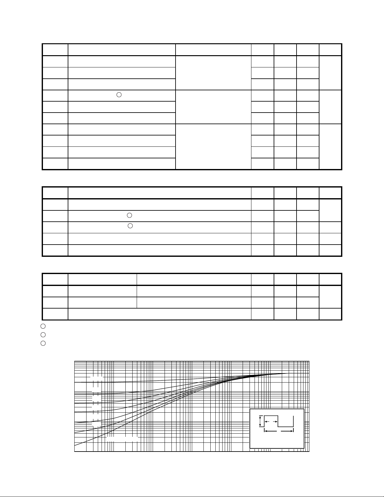
Repetitive Rating: Pulse width limited by maximum junction temperature. See Transient Thermal Impedance Curve. (Fig.1)
2
Pulse Test: Pulse width < 380 µS, Duty Cycle < 2%
3
See MIL-STD-750 Method 3471
APT Reserves the right to change, without notice, the specifications and information contained herein.
050-6107 Rev B
Characteristic
Safe Operating Area
Safe Operating Area
Inductive Current Clamped
LM
1.0
0.5
D=0.5
0.1
0.05
0.01
0.005
0.001
10
0.2
0.05
0.02
0.01
-5
FIGURE 1, MAXIMUM EFFECTIVE TRANSIENT THERMAL IMPEDANCE, JUNCTION-TO-CASE vs PULSE DURATION
0.1
SINGLE PULSE
-4
10
Test Conditions
V
= 0.4 V
DS
I
= ID [Cont.], VDS = PD / ID [Cont.], t = 1 Sec.
DS
-3
10
RECTANGULAR PULSE DURATION (SECONDS)
, IDS = PD / 0.4 V
DSS
10
, t = 1 Sec.
DSS
-2
10
-1
MIN TYP MAX
310
310
76
Note:
DM
P
Duty Factor D =
Peak TJ = PDM x Z
1.0 10
UNIT
Watts
Amps
t
1
t
2
t
1
/
t
2
+ T
θJC
C
 Loading...