

Advanced Power Technology APT APT6030BVFR Datasheet
APT6030BVFR
600V 21A 0.300W
POWER MOS V
®
Power MOS V® is a new generation of high voltage N-Channel enhancement
FREDFET
TO-247
mode power MOSFETs. This new technology minimizes the JFET effect,
increases packing density and reduces the on-resistance. Power MOS V
®
also achieves faster switching speeds through optimized gate layout.
• Fast Recovery Body Diode • 100% Avalanche Tested
D
• Lower Leakage • Popular TO-247 Package
G
• Faster Switching
S
MAXIMUM RATINGS All Ratings: TC = 25°C unless otherwise specified.
Symbol
V
DSS
I
D
I
DM
V
GS
V
GSM
P
D
TJ,T
STG
T
L
I
AR
E
AR
E
AS
Parameter
Drain-Source Voltage
Continuous Drain Current @ T
Pulsed Drain Current
Gate-Source Voltage Continuous
Gate-Source Voltage Transient
Total Power Dissipation @ TC = 25°C
Linear Derating Factor
Operating and Storage Junction Temperature Range
Lead Temperature: 0.063" from Case for 10 Sec.
Avalanche Current
Repetitive Avalanche Energy
Single Pulse Avalanche Energy
1
1
(Repetitive and Non-Repetitive)
= 25°C
C
1
4
APT6030BVFR
600
21
84
±30
±40
300
2.4
-55 to 150
300
21
30
1300
UNIT
Volts
Amps
Volts
Watts
W/°C
°C
Amps
mJ
STATIC ELECTRICAL CHARACTERISTICS
USA 405 S.W. Columbia Street Bend, Oregon 97702-1035 Phone: (541) 382-8028 FAX: (541) 388-0364
EUROPE Chemin de Magret F-33700 Merignac - France Phone: (33)5 57 9215 15 FAX: (33)556 47 9761
PRELIMINARY
Symbol
BV
I
D(on)
R
DS(on)
I
DSS
I
GSS
V
GS(th)
Characteristic / Test Conditions
Drain-Source Breakdown Voltage (V
DSS
On State Drain Current
Drain-Source On-State Resistance
Zero Gate Voltage Drain Current (VDS = V
Zero Gate Voltage Drain Current (V
Gate-Source Leakage Current (VGS = ±30V, V
Gate Threshold Voltage (VDS = VGS, ID = 1.0mA)
CAUTION: These Devices are Sensitive to Electrostatic Discharge. Proper Handling Procedures Should Be Followed.
2
(V
DS
APT Website - http://www.advancedpower.com
= 0V, ID = 250µA)
GS
> I
x R
D(on)
2
(VGS = 10V, 0.5 I
= 0.8 V
DS
Max, VGS = 10V)
DS(on)
D[Cont.]
, VGS = 0V)
DSS
, VGS = 0V, TC = 125°C)
DSS
= 0V)
DS
)
MIN TYP MAX
600
21
24
1000
±100
0.30
250
UNIT
Volts
Amps
Ohms
µA
nA
Volts
050-5944 Rev - 1- 2000
DYNAMIC CHARACTERISTICS APT6030BVFR
Note:
Duty Factor D =
t
1
/
t
2
Peak TJ = PDM x Z
θJC
+ T
C
t
1
t
2
P
DM
Symbol
C
iss
C
oss
C
rss
Q
g
Q
gs
Q
gd
td(on)
t
r
td(off)
t
f
Characteristic
Input Capacitance
Output Capacitance
Reverse Transfer Capacitance
Total Gate Charge
3
Gate-Source Charge
Gate-Drain ("Miller") Charge
Turn-on Delay Time
Rise Time
Turn-off Delay Time
Fall Time
Test Conditions
V
= 0V
GS
= 25V
V
DS
f = 1 MHz
V
= 10V
GS
= 0.5 V
V
DD
ID = I
[Cont.] @ 25°C
D
V
= 15V
GS
VDD = 0.5 V
ID = I
[Cont.] @ 25°C
D
R
= 1.6W
G
DSS
DSS
MIN TYP MAX
3750 4500
430 600
160 240
150 225
18 27
60 90
12 24
10 20
47 75
816
UNIT
pF
nC
ns
SOURCE-DRAIN DIODE RATINGS AND CHARACTERISTICS
Symbol
I
I
SM
V
dv
t
Characteristic / Test Conditions
Continuous Source Current (Body Diode)
S
Pulsed Source Current
Diode Forward Voltage
SD
Peak Diode Recovery dv/
/
dt
1
(Body Diode)
2
dt
Reverse Recovery Time
rr
= -ID [Cont.], di/dt = 100A/µs)
(I
S
(VGS = 0V, IS = -ID [Cont.])
5
Reverse Recovery Charge
Q
rr
(IS = -ID [Cont.], di/dt = 100A/µs)
Peak Recovery Current
I
RRM
(IS = -ID [Cont.], di/dt = 100A/µs)
THERMAL CHARACTERISTICS
Symbol
R
qJC
R
1
Repetitive Rating: Pulse width limited by maximum junction
temperature.
2
Pulse Test: Pulse width < 380 µS, Duty Cycle < 2%
Characteristic
Junction to Case
Junction to Ambient
qJA
PRELIMINARY
T
= 25°C 205 250
j
T
= 125°C 415 525
j
T
= 25°C 1.5
j
T
= 125°C 5.5
j
T
= 25°C 13
j
T
= 125°C 23
j
3
See MIL-STD-750 Method 3471
4
Starting T
5
IS £ ID [Cont.],
+25°C, L = 5.90mH, R
j
=
di
/
= 100A/µs, T
dt
MIN TYP MAX
21
84
1.3
5
MIN TYP MAX
0.42
40
25W, Peak IL = 21A
G
=
150°C, R
j
£
= 2.0W VR = 200V.
G
UNIT
Amps
Volts
V/ns
ns
µC
Amps
UNIT
°C/W
050-5944 Rev - 1- 2000
,
APT Reserves the right to change, without notice, the specifications and information contained herein.
0.5
D=0.5
0.1
0.05
0.01
0.005
, THERMAL IMPEDANCE (°C/W)
JC
q
Z
0.001
-5
10
0.2
0.1
0.05
0.02
0.01
SINGLE PULSE
-4
10
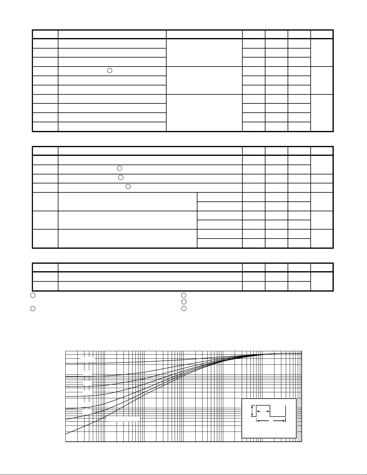
FIGURE 1, MAXIMUM EFFECTIVE TRANSIENT THERMAL IMPEDANCE, JUNCTION-TO-CASE vs PULSE DURATION
-3
10
RECTANGULAR PULSE DURATION (SECONDS)
-2
10
10
-1
1.0 10
 Loading...