

Advanced Power Technology APT APT50M50L2FLL Datasheet
APT50M50L2FLL
500V 89A 0.050W
POWER MOS 7
TM
Power MOS 7TM is a new generation of low loss, high voltage, N-Channel
enhancement mode power MOSFETS. Both conduction and switching
losses are addressed with Power MOS 7
and Qg. Power MOS 7
TM
combines lower conduction and switching losses
TM
by significantly lowering R
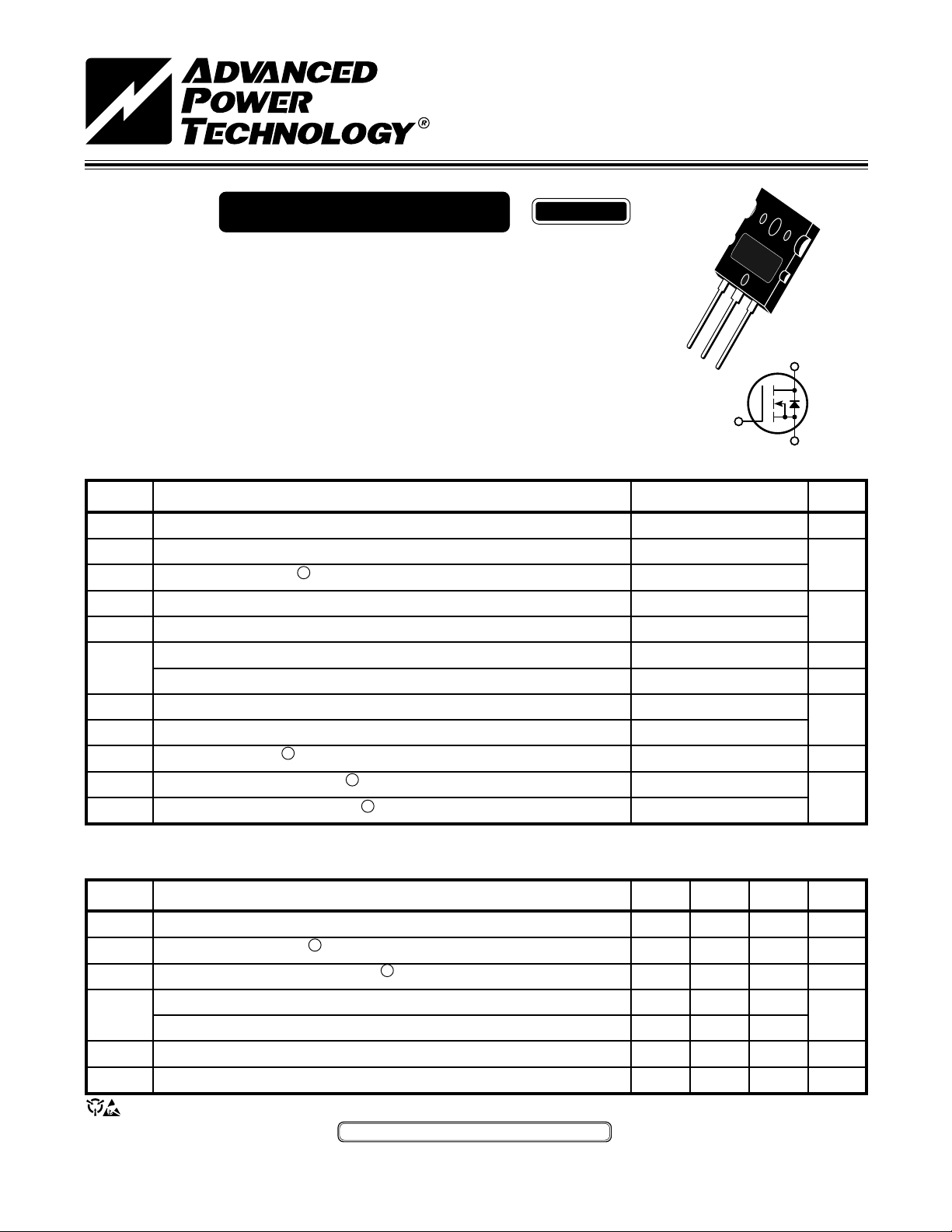
FREDFET
TO-264
Max
DS(ON)
along with exceptionally fast switching speeds inherent with APT's
patented metal gate structure.
• Lower Input Capacitance •Increased Power Dissipation
D
• Lower Miller Capacitance •Easier To Drive
• Lower Gate Charge, Qg • Popular TO-264
MAXIMUM RATINGS All Ratings: TC = 25°C unless otherwise specified.
Symbol
V
DSS
I
I
DM
V
V
GSM
P
TJ,T
T
I
AR
E
E
STATIC ELECTRICAL CHARACTERISTICS
Parameter
Drain-Source Voltage
Continuous Drain Current @ T
D
Pulsed Drain Current
Gate-Source Voltage Continuous
GS
Gate-Source Voltage Transient
Total Power Dissipation @ T
D
Linear Derating Factor
Operating and Storage Junction Temperature Range
STG
Lead Temperature: 0.063" from Case for 10 Sec.
L
Avalanche Current
Repetitive Avalanche Energy
AR
Single Pulse Avalanche Energy
AS
1
1
(Repetitive and Non-Repetitive)
ADVANCE TECHNICAL
= 25°C
C
= 25°C
C
1
4
INFORMATION
MAX Package
APT50M50L2FLL
-55 to 150
500
89
356
±30
±40
890
7.12
300
89
50
3200
G
S
UNIT
Volts
Amps
Volts
Watts
W/°C
°C
Amps
mJ
Symbol
BV
I
D(on)
R
DS(on)
I
DSS
I
GSS
V
GS(th)
USA 405 S.W. Columbia Street Bend, Oregon 97702-1035 Phone: (541) 382-8028 FAX: (541) 388-0364
EUROPE Chemin de Magret F-33700 Merignac - France Phone: (33 ) 5 57 9215 15 FAX: (33) 5 56 47 97 61
Characteristic / Test Conditions
Drain-Source Breakdown Voltage (V
DSS
On State Drain Current
Drain-Source On-State Resistance
Zero Gate Voltage Drain Current (VDS = V
Zero Gate Voltage Drain Current (V
Gate-Source Leakage Current (VGS = ±30V, V
Gate Threshold Voltage (VDS = VGS, ID = 5mA)
CAUTION: These Devices are Sensitive to Electrostatic Discharge. Proper Handling Procedures Should Be Followed.
2
(V
DS
APT Website - http://www.advancedpower.com
= 0V, ID = 250µA)
GS
> I
x R
D(on)
2
(VGS = 10V, 0.5 I
= 0.8 V
DS
Max, VGS = 10V)
DS(on)
D[Cont.]
, VGS = 0V)
DSS
, VGS = 0V, TC = 125°C)
DSS
= 0V)
DS
)
MIN TYP MAX
500
89
35
0.050
250
1000
±100
UNIT
Volts
Amps
Ohms
µA
nA
Volts
050-7115 Rev- 9-2001
DYNAMIC CHARACTERISTICS
Symbol
C
iss
C
oss
C
rss
Q
g
Q
gs
Q
gd
td(on)
t
r
td(off)
t
f
Characteristic
Input Capacitance
Output Capacitance
Reverse Transfer Capacitance
Total Gate Charge
3
Gate-Source Charge
Gate-Drain ("Miller") Charge
Turn-on Delay Time
Rise Time
Turn-off Delay Time
Fall Time
Test Conditions
V
VDS = 25V
f = 1 MHz
VGS = 10V
VDD = 0.5 V
ID = I
[Cont.] @ 25°C
D
V
GS
VDD = 0.5 V
ID = I
[Cont.] @ 25°C
D
RG =0.6W
SOURCE-DRAIN DIODE RATINGS AND CHARACTERISTICS
= 0V
GS
= 15V
DSS
DSS
APT50M50L2FLL
MIN TYP MAX
9840
2030
153
246
65
112
24
22
56
8
UNIT
pF
nC
ns
Symbol
I
I
SM
V
dv
t
Characteristic / Test Conditions
Continuous Source Current (Body Diode)
S
Pulsed Source Current
Diode Forward Voltage
SD
Peak Diode Recovery dv/
/
dt
ADVANCE TECHNICAL
1
(Body Diode)
2
dt
Reverse Recovery Time
rr
= -ID [Cont.], di/dt = 100A/µs)
(I
S
(VGS = 0V, IS = -ID [Cont.])
5
INFORMATION
Reverse Recovery Charge
Q
rr
(IS = -ID [Cont.], di/dt = 100A/µs)
Peak Recovery Current
I
RRM
(IS = -ID [Cont.], di/dt = 100A/µs)
THERMAL CHARACTERISTICS
Symbol
R
qJC
R
qJA
1
Repetitive Rating: Pulse width limited by maximum junction
temperature.
2
Pulse Test: Pulse width < 380 µs, Duty Cycle < 2%
APT Reserves the right to change,
without notice, the specifications
and information contained herein.
Characteristic
Junction to Case
Junction to Ambient
TO-264 MAXTM(L2) Package Outline
4.60 (.181)
5.21 (.205)
1.80 (.071)
2.01 (.079)
MIN TYP MAX
89
356
1.3
15
T
= 25°C 300
j
T
= 125°C 600
j
T
= 25°C 2.6
j
T
= 125°C 10
j
T
= 25°C 17
j
T
= 125°C 34
j
MIN TYP MAX
0.14
40
3
See MIL-STD-750 Method 3471
4
Starting T
5dv
/
dt
device itself. I
+25°C, L = 0.81mH, R
j
=
numbers reflect the limitations of the test circuit rather than the
£ -I
S
19.51 (.768)
20.50 (.807)
D[Cont.
di
/
dt
]
25W, Peak IL = 89A
G
=
£ 700A/µs V
£ V
R
DSS
T
UNIT
Amps
Volts
V/ns
ns
µC
Amps
UNIT
°C/W
£ 150°C
J
5.79 (.228)
6.20 (.244)
25.48 (1.003)
Drain
Dimensions in Millimeters and (Inches)
APT's devices are covered by one or more of the following U.S.patents: 4,895,810 5,045,903 5,089,434 5,182,234 5,019,522 5,262,336
050-7115 Rev- 9-2001
26.49 (1.043)
2.29 (.090)
2.29 (.090)
2.69 (.106)
19.81 (.780)
21.39 (.842)
0.48 (.019)
0.84 (.033)
2.59 (.102)
3.00 (.118)
5,256,583 4,748,103 5,283,202 5,231,474 5,434,095 5,528,058
0.76 (.030)
1.30 (.051)
2.79 (.110)
3.18 (.125)
5.45 (.215) BSC
2-Plcs.
2.69 (.106)
Gate
Drain
Source
 Loading...