

Advanced Power Technology APT APT5040CNR Datasheet
G
D
TO-254
S
TM
POWER MOS IV
APT5040CNR 500V 13.0A 0.400Ω
Avalanche Rated
N - CHANNEL ENHANCEMENT MODE HIGH VOLTAGE POWER MOSFETS
•Faster Switching •100% Avalanche Tested •Popular TO-254 Package
•Low Gate Charge •Similar to the 2N7228, JX2N7228 and JV2N7228
MAXIMUM RATINGS All Ratings: TC = 25°C unless otherwise specified.
Symbol
V
DSS
I
D
I
DM
V
GS
V
GSM
P
D
TJ,T
STG
T
L
I
AR
E
AR
E
AS
Parameter
Drain-Source Voltage
Continuous Drain Current @ T
Pulsed Drain Current
1
= 25°C
C
Gate-Source Voltage Continuous
Gate-Source Voltage Transient
Total Power Dissipation @ TC = 25°C
Linear Derating Factor
Operating and Storage Junction Temperature Range
Lead Temperature: 0.063" from Case for 10 Sec.
1
Avalanche Current
Repetitive Avalanche Energy
Single Pulse Avalanche Energy
(Repetitive and Non-Repetitive)
1
3
APT5040CNR
500
13
52
±30
±40
150
1.2
-55 to 150
300
13
20
800
UNIT
Volts
Amps
Volts
Watts
W/°C
°C
Amps
mJ
STATIC ELECTRICAL CHARACTERISTICS
Symbol
BV
I
D(on)
R
DS(on)
I
DSS
I
GSS
V
GS(th)
USA
405 S.W. Columbia Street Bend, Oregon 97702-1035 Phone: (541) 382-8028 FAX: (541) 388-0364
EUROPE
Avenue J.F. Kennedy Bât B4 Parc Cadéra Nord F-33700 Merignac - France Phone: (33) 5 5792 15 15 FAX: (33) 556 47 97 61
Characteristic / Test Conditions
Drain-Source Breakdown Voltage (V
DSS
On State Drain Current
2
(V
DS
Drain-Source On-State Resistance
Zero Gate Voltage Drain Current (VDS = V
Zero Gate Voltage Drain Current (V
Gate-Source Leakage Current (VGS = ±30V, V
= 0V, ID = 250µA)
GS
> I
x R
D(on)
2
(VGS = 10V, 0.5 I
= 0.8 V
DS
Max, VGS = 10V)
DS(on)
D[Cont.]
, VGS = 0V)
DSS
, VGS = 0V, TC = 125°C)
DSS
= 0V)
DS
)
Gate Threshold Voltage (VDS = VGS, ID = 1.0mA)
CAUTION: These Devices are Sensitive to Electrostatic Discharge. Proper Handling Procedures Should Be Followed.
APT Website - http://www.advancedpower.com
MIN TYP MAX
500
13
24
0.40
250
1000
±100
UNIT
Volts
Amps
Ohms
µA
nA
Volts
050-5016 Rev -
DYNAMIC CHARACTERISTICS
Note:
Duty Factor D =
t
1
/
t
2
Peak TJ = PDM x Z
θJC
+ T
C
t
1
t
2
P
DM
APT5040CNR
Symbol
C
DC
C
iss
C
oss
C
rss
Q
g
Q
gs
Q
gd
td(on)
t
r
td(off)
t
f
Characteristic
Drain-to-Case Capacitance
Input Capacitance
Output Capacitance
Reverse Transfer Capacitance
Total Gate Charge
Gate-Source Charge
Gate-Drain ("Miller") Charge
Turn-on Delay Time
Rise Time
Turn-off Delay Time
Fall Time
Test Conditions
f = 1 MHz
V
VDS = 25V
f = 1 MHz
VGS = 10V
VDD = 0.5 V
ID = ID [Cont.] @ 25°C
VGS = 10V
VDD = 0.5 V
ID = ID [Cont.] @ 25°C
RG = 1.80Ω
SOURCE-DRAIN DIODE RATINGS AND CHARACTERISTICS
Symbol
I
I
SM
V
t
Q
Characteristic / Test Conditions
Continuous Source Current (Body Diode)
S
1
Pulsed Source Current
Diode Forward Voltage 2 (VGS = 0V, IS = -ID [Cont.])
SD
Reverse Recovery Time (IS = -ID [Cont.], dlS/dt = 100A/µs)
rr
Reverse Recovery Charge (IS = -ID [Cont.], dlS/dt = 100A/µs)
rr
(Body Diode)
GS
= 0V
DSS
DSS
MIN TYP MAX
15 22
1430 1800
330 465
130 200
71 105
8.7 12
37 55
14 28
21 42
44 66
15 30
MIN TYP MAX
13
52
1.3
296 592
4.4 8.8
UNIT
pF
nC
ns
UNIT
Amps
Volts
ns
µC
050-5016 Rev -
THERMAL CHARACTERISTICS
Symbol
R
θJC
R
θJA
1
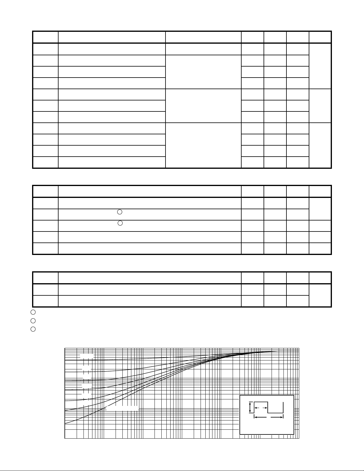
Repetitive Rating: Pulse width limited by maximum junction temperature. See Transient Thermal Impedance Curve. (Fig.1)
2
Pulse Test: Pulse width < 380 µS, Duty Cycle < 2%
3
Starting T
APT Reserves the right to change, without notice, the specifications and information contained herein.
Characteristic
Junction to Case
Junction to Ambient
+25°C, L = 9.47mH, R
j
=
1.0
0.5
0.1
0.05
0.01
0.005
, THERMAL IMPEDANCE (°C/W)
JC
θ
Z
0.001
-5
10
25Ω, Peak IL = 13A
G
=
D=0.5
0.2
0.1
0.05
0.02
0.01
FIGURE 1, MAXIMUM EFFECTIVE TRANSIENT THERMAL IMPEDANCE, JUNCTION-TO-CASE vs PULSE DURATION
SINGLE PULSE
-4
10
-3
10
RECTANGULAR PULSE DURATION (SECONDS)
-2
10
-1
10
MIN TYP MAX
1.0 10
UNIT
0.80
W/°C
50
 Loading...