Advanced Power Technology APT APT20M13PVR Datasheet

APT20M13PVR
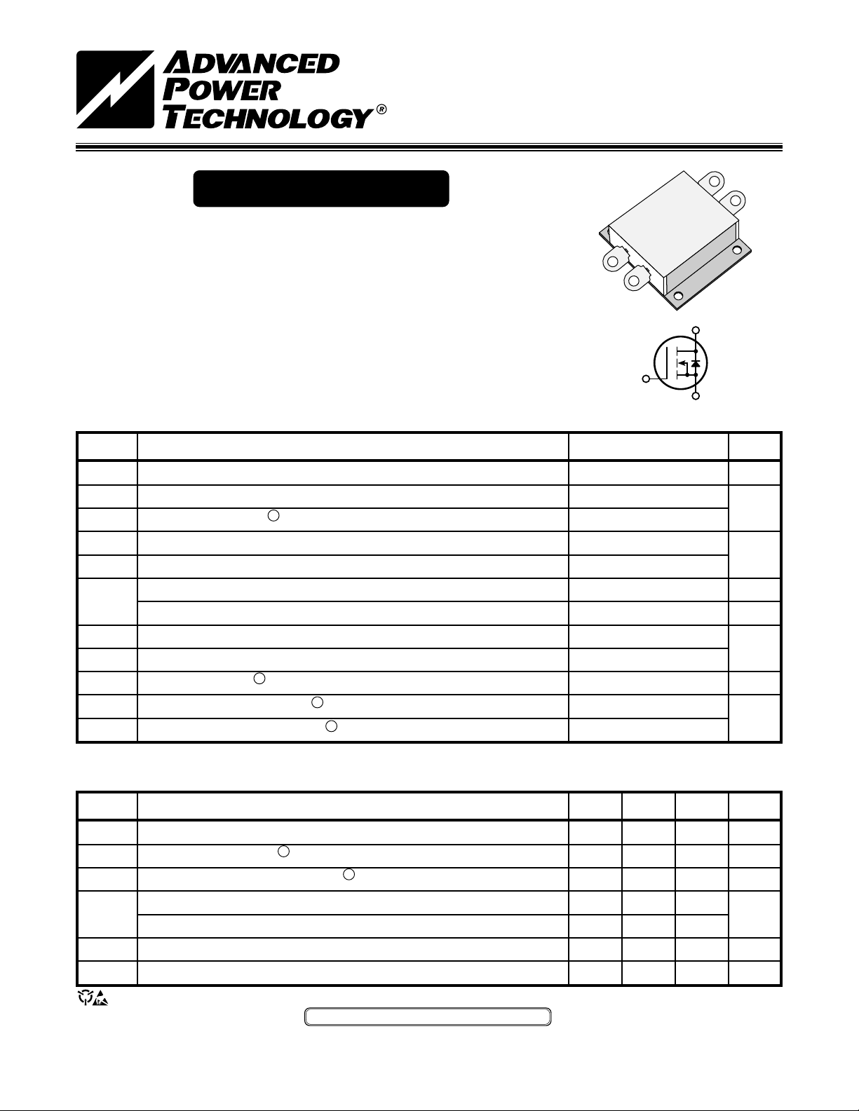
200V 146A 0.013Ω
POWER MOS V
®
Power MOS V® is a new generation of high voltage N-Channel enhancement
mode power MOSFETs. This new technology minimizes the JFET effect,
®
increases packing density and reduces the on-resistance. Power MOS V
also
achieves faster switching speeds through optimized gate layout.
• Faster Switching • 100% Avalanche Tested
• Lower Leakage • New High Power P-Pack Package
MAXIMUM RATINGS All Ratings: TC = 25°C unless otherwise specified.
Symbol
V
DSS
I
D
I
DM
V
GS
V
GSM
P
D
TJ,T
STG
T
L
I
AR
E
AR
E
AS
Parameter
Drain-Source Voltage
Continuous Drain Current @ T
Pulsed Drain Current
Gate-Source Voltage Continuous
Gate-Source Voltage Transient
Total Power Dissipation @ TC = 25°C
Linear Derating Factor
Operating and Storage Junction Temperature Range
Lead Temperature: 0.063" from Case for 10 Sec.
Avalanche Current
Repetitive Avalanche Energy
Single Pulse Avalanche Energy
1
1
(Repetitive and Non-Repetitive)
= 25°C
C
1
4
APT20M13PVR
P-Pack
G
200
146
584
±30
±40
625
5.0
-55 to 150
300
146
30
3600
D
S
UNIT
Volts
Amps
Volts
Watts
W/°C
°C
Amps
mJ
STATIC ELECTRICAL CHARACTERISTICS
Symbol
BV
I
D(on)
R
DS(on)
I
DSS
I
GSS
V
GS(th)
USA
405 S.W. Columbia Street Bend, Oregon 97702-1035 Phone: (541) 382-8028 FAX: (541) 388-0364
EUROPE
Avenue J.F. Kennedy Bât B4 Parc Cadéra Nord F-33700 Merignac - France Phone: (33)5 57 9215 15 FAX: (33) 5 56 4797 61
Characteristic / Test Conditions
Drain-Source Breakdown Voltage (V
DSS
On State Drain Current
Drain-Source On-State Resistance
Zero Gate Voltage Drain Current (VDS = V
Zero Gate Voltage Drain Current (V
Gate-Source Leakage Current (VGS = ±30V, V
Gate Threshold Voltage (VDS = VGS, ID = 5mA)
CAUTION: These Devices are Sensitive to Electrostatic Discharge. Proper Handling Procedures Should Be Followed.
PRELIMINARY
2
(V
DS
APT Website - http://www.advancedpower.com
= 0V, ID = 250µA)
GS
> I
x R
D(on)
2
(VGS = 10V, 0.5 I
= 0.8 V
DS
Max, VGS = 10V)
DS(on)
D[Cont.]
, VGS = 0V)
DSS
, VGS = 0V, TC = 125°C)
DSS
= 0V)
DS
)
MIN TYP MAX
200
146
24
0.013
100
500
±100
UNIT
Volts
Amps
Ohms
µA
nA
Volts
050-5834 Rev -

DYNAMIC CHARACTERISTICS
APT20M13PVR
Symbol
C
iss
C
oss
C
rss
Q
g
Q
gs
Q
gd
t
d(on)
t
r
t
d(off)
t
f
Characteristic
Input Capacitance
Output Capacitance
Reverse Transfer Capacitance
Total Gate Charge
3
Gate-Source Charge
Gate-Drain ("Miller") Charge
Turn-on Delay Time
Rise Time
Turn-off Delay Time
Fall Time
Test Conditions
V
VDS = 25V
f = 1 MHz
V
GS
VDD = 0.5 V
ID = I
D[Cont.]
VGS = 15V
VDD = 0.5 V
ID = I
D[Cont.]
RG = 0.6Ω
SOURCE-DRAIN DIODE RATINGS AND CHARACTERISTICS
Symbol
I
I
SM
V
t
Q
Characteristic / Test Conditions
Continuous Source Current (Body Diode)
S
1
Pulsed Source Current
Diode Forward Voltage 2 (VGS = 0V, IS = -I
SD
Reverse Recovery Time (IS = -I
rr
Reverse Recovery Charge (I
rr
(Body Diode)
S
= -I
, dlS/dt = 100A/µs)
D[Cont.]
, dlS/dt = 100A/µs)
D[Cont.]
D[Cont.]
)
= 0V
GS
= 10V
DSS
@ 25°C
DSS
@ 25°C
MIN TYP MAX
18000
4100
1350
630
95
290
20
40
75
10
MIN TYP MAX
146
584
1.5
460
7
UNIT
pF
nC
ns
UNIT
Amps
Volts
ns
µC
THERMAL CHARACTERISTICS
Symbol
R
θJC
R
1
Repetitive Rating: Pulse width limited by maximum junction
temperature.
2
Pulse Test: Pulse width < 380 µS, Duty Cycle < 2%
APT Reserves the right to change, without notice, the specifications and information contained herein.
Characteristic
Junction to Case
Junction to Ambient
θJA
3
PRELIMINARY
See MIL-STD-750 Method 3471
4
Starting T
+25°C, L = .34mH, R
j
=
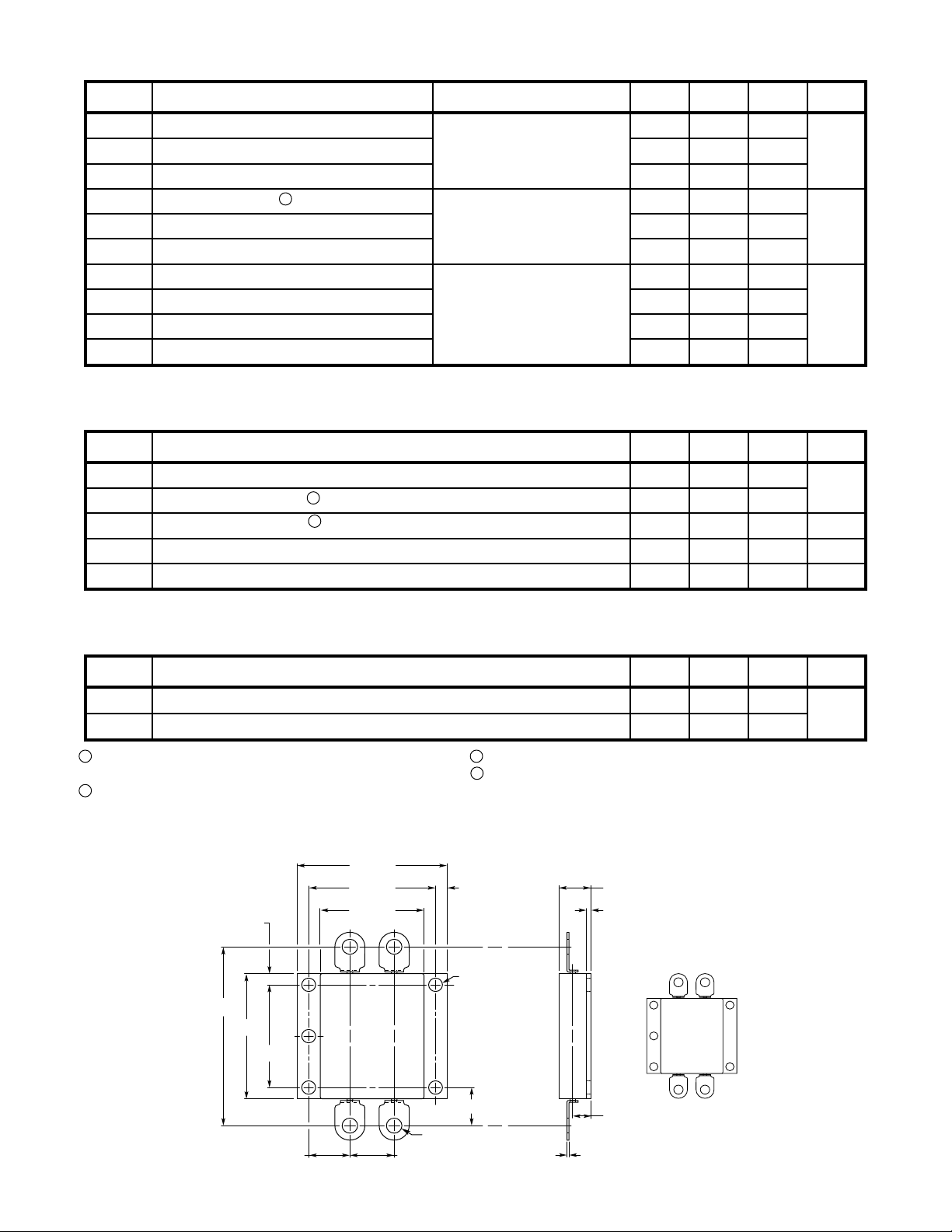
P-Pack Package Outline
41.53 (1.635)
41.02 (1.615)
3.43 (.135)
2.92 (.115)
(4-Places)
51.05 (2.01)
50.55 (1.99)
35.81 (1.41)
35.31 (1.39)
29.34 (1.155)
29.08 (1.145)
35.18 (1.385)
34.67 (1.365)
28.70 (1.130)
28.45 (1.120)
3.43 (.135)
2.92 (.115)
(4-Places)
4.06 (.160)
3.81 (.150)
(5 Places)
MIN TYP MAX
G
=
9.27 (.365)
8.64 (.340)
1.40 (.055)
1.02 (.040)
Drain Gate
0.20
40
25Ω, Peak IL =146A
Source Source Sense
UNIT
°C/W
050-5834 Rev -
11.63 (.458)
11.13 (.438)
10.92 (.430)
10.67 (.420)
4.39 (.173)
4.14 (.163)
(4 Places)
12.45 (.490)
11.94 (.470)
Dimensions in Millimeters and (Inches)
5.33 (.210)
4.83 (.190)
.635 (.025)
.381 (.015)
 Loading...