

Advanced Power Technology APT APT1004RGN Datasheet
G
D
TO-257
S
TM
APT1004RGN 1000V 3.3A 4.00Ω
POWER MOS IV
N - CHANNEL ENHANCEMENT MODE HIGH VOLTAGE POWER MOSFETS
MAXIMUM RATINGS All Ratings: TC = 25°C unless otherwise specified.
Symbol
V
DSS
I
D
I
DM
V
GS
P
D
TJ,T
STG
T
L
Parameter
Drain-Source Voltage
Continuous Drain Current @ T
Pulsed Drain Current
1
= 25°C
C
Gate-Source Voltage
Total Power Dissipation @ T
= 25°C
C
Linear Derating Factor
Operating and Storage Junction Temperature Range
Lead Temperature: 0.063" from Case for 10 Sec.
APT1004RGN
1000
3.3
13.2
±30
100
0.8
-55 to 150
300
UNIT
Volts
Amps
Volts
Watts
W/°C
°C
STATIC ELECTRICAL CHARACTERISTICS
Symbol
BV
ID(ON)
R
DS
I
DSS
I
GSS
VGS(TH)
Characteristic / Test Conditions
Drain-Source Breakdown Voltage (V
DSS
On State Drain Current
(ON)
Drain-Source On-State Resistance
2
(V
> ID(ON) x RDS(ON) Max, VGS = 10V)
DS
Zero Gate Voltage Drain Current (VDS = V
Zero Gate Voltage Drain Current (V
Gate-Source Leakage Current (VGS = ±30V, V
Gate Threshold Voltage (VDS = VGS, ID = 1.0mA)
= 0V, ID = 250µA)
GS
2
(VGS = 10V, 0.5 ID [Cont.])
= 0.8 V
DS
SAFE OPERATING AREA CHARACTERISTICS
Symbol
SOA1
SOA2
I
LM
Characteristic
Safe Operating Area
Safe Operating Area
Inductive Current Clamped
= 0.4 V
V
DS
DSS
IDS = ID [Cont.], VDS = PD / ID [Cont.], t = 1 Sec.
, VGS = 0V)
DSS
, VGS = 0V, TC = 125°C)
DSS
= 0V)
DS
Test Conditions
, IDS = PD / 0.4 V
, t = 1 Sec.
DSS
MIN TYP MAX
1000
3.3
4.00
250
1000
±100
2 4
MIN TYP MAX
100
100
3.3
UNIT
Volts
Amps
Ohms
µA
nA
Volts
UNIT
Watts
Amps
CAUTION: These Devices are Sensitive to Electrostatic Discharge. Proper Handling Procedures Should Be Followed.
USA
405 S.W. Columbia Street Bend, Oregon 97702-1035 Phone: (541) 382-8028 FAX: (541) 388-0364
APT Website - http://www.advancedpower.com
EUROPE
Avenue J.F. Kennedy Bât B4 Parc Cadéra Nord F-33700 Merignac - France Phone: (33)5 57 92 15 15 FAX: (33)5 56 47 97 61
050-0019 Rev B
DYNAMIC CHARACTERISTICS
Note:
Duty Factor D =
t
1
/
t
2
Peak TJ = PDM x Z
θJC
+ T
C
t
1
t
2
P
DM
APT1004RGN
Symbol
C
DC
C
iss
C
oss
C
rss
Q
g
Q
gs
Q
gd
td(on)
t
r
td(off)
t
f
Characteristic
Drain-to-Case Capacitance
Input Capacitance
Output Capacitance
Reverse Transfer Capacitance
Total Gate Charge
Gate-Source Charge
Gate-Drain ("Miller") Charge
Turn-on Delay Time
Rise Time
Turn-off Delay Time
Fall Time
Test Conditions
f = 1 MHz
V
VDS = 25V
f = 1 MHz
VGS = 10V
VDD = 0.5 V
ID = ID [Cont.] @ 25°C
VGS = 10V
VDD = 0.5 V
ID = ID [Cont.] @ 25°C
RG = 1.8Ω
SOURCE-DRAIN DIODE RATINGS AND CHARACTERISTICS
Symbol
I
I
SM
V
t
Q
Characteristic / Test Conditions
Continuous Source Current (Body Diode)
S
1
Pulsed Source Current
Diode Forward Voltage 2 (VGS = 0V, IS = -ID [Cont.])
SD
Reverse Recovery Time (IS = -ID [Cont.], dlS/dt = 100A/µs)
rr
Reverse Recovery Charge (IS = -ID [Cont.], dlS/dt = 100A/µs)
rr
(Body Diode)
GS
= 0V
DSS
DSS
MIN TYP MAX
812
805 950
115 160
37 60
35 55
4.3 7
18 27
10 20
12 24
33 50
16 32
MIN TYP MAX
3.3
13.2
1.3
290 580
1.65 3.3
UNIT
pF
nC
ns
UNIT
Amps
Volts
ns
µC
050-0019 Rev B
THERMAL CHARACTERISTICS
Symbol
R
θJC
R
θJA
1
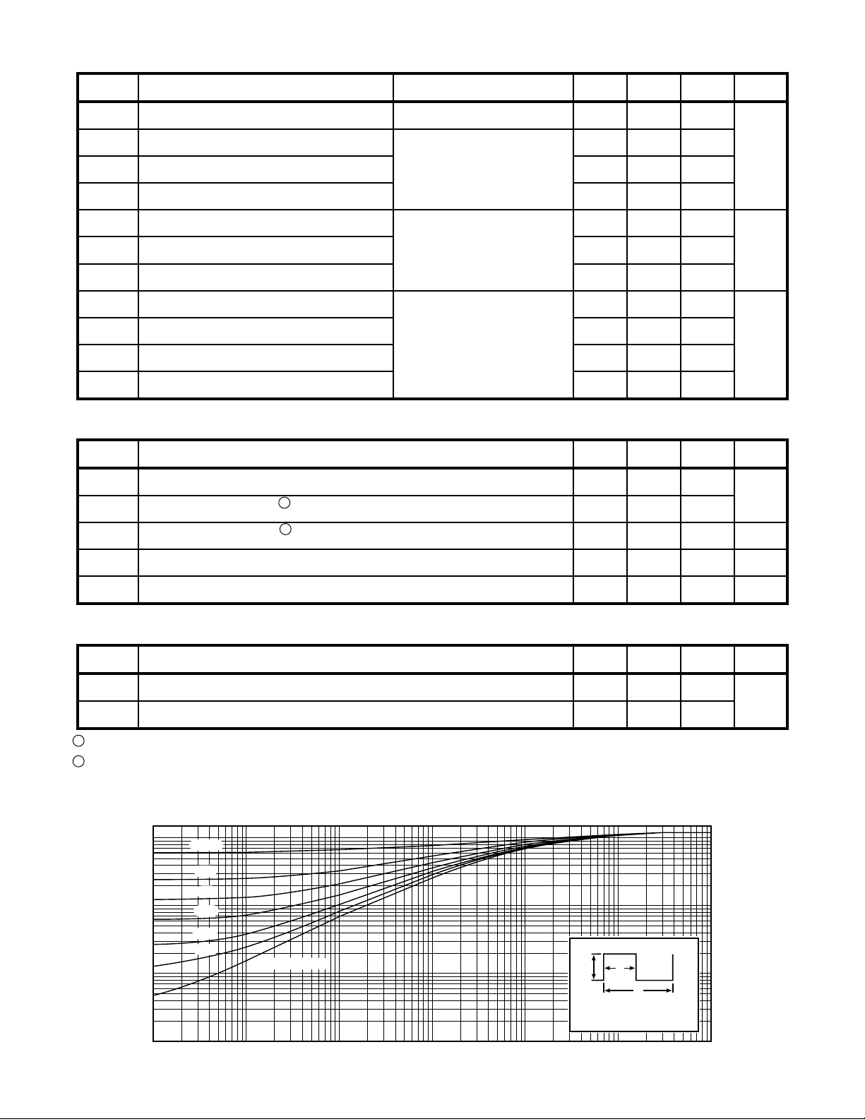
Repetitive Rating: Pulse width limited by maximum junction temperature. See Transient Thermal Impedance Curve. (Fig.1)
2
Pulse Test: Pulse width < 380 µS, Duty Cycle < 2%
APT Reserves the right to change, without notice, the specifications and information contained herein.
Characteristic
Junction to Case
Junction to Ambient
1.5
1.0
0.5
0.1
0.05
0.01
, THERMAL IMPEDANCE (°C/W)
0.005
JC
θ
Z
0.001
-5
10
D=0.5
0.2
0.1
0.05
0.02
0.01
SINGLE PULSE
-4
10
FIGURE 1, MAXIMUM EFFECTIVE TRANSIENT THERMAL IMPEDANCE, JUNCTION-TO-CASE vs PULSE DURATION
-3
10
RECTANGULAR PULSE DURATION (SECONDS)
-2
10
-1
10
MIN TYP MAX
1.0 10
UNIT
1.20
W/°C
80
 Loading...