

Page 1

www.DataSheet4U.com
APTM20TAM16FP
–
S
MOSFET Power Module
VBUS1 VBUS2 VBUS3
G1
S1
G2
S2
0/VBUS1
Triple phase leg
G5
S5
V
G6
S6
0/VBUS3
VBUS 3
G3
S3
0/VBUS 3
S4
G4
WV
VBUS 1
0/VBUS 1
G3
S3
U
G4
S4
0/VBUS2
VBUS 2
G1
S1
0/VBUS 2
S2
G2
U
W
G5
S5
S6
G6
Absolute maximum ratings
ymbol Parameter Max ratings Unit
V
Drain - Source Breakdown Voltage 200 V
DSS
ID Continuo us Drain Current
IDM Pulsed Drain current 416
VGS Gate - Source Voltage ±30 V
R
Drain - Source ON Resistance 16
DSon
PD Maximum Power Dissipation Tc = 25°C 390 W
IAR Avalanche current (repetitive and non repetitive) 100 A
EAR Repetitive Avalanche Energy 50
EAS Single Pulse Avalanche Energy 3000
These Devices are sensitive to Electrostatic Discharge. Proper Handing Procedures Should Be Followed.
V
R
I
= 200V
DSS
= 16mΩ max @ Tj = 25°C
DSon
= 104A @ Tc = 25°C
D
Application
• Welding converters
• Switched Mode Power Supplies
• Uninterruptible Power Supplies
• Motor control
Features
• Power MOS 7® FREDFETs
- Low R
DSon
- Low input and Miller capacitance
- Low gate charge
- Fast intrinsic reverse diode
- Avalanche energy rated
- Very rugged
• Kelvin source for easy drive
• Very low stray inductance
- Symme trical design
- Lead frames for power connections
• High level of integration
Benefits
• Outsta ndi ng performa nce at hi gh freq uenc y opera tion
• Direct mounting to heatsink (isolated package)
• Low junction to case thermal resistance
• Solderable terminals both for power and signal for
easy PCB mounting
• Very low (12mm) profile
• Each leg can be easily paralleled to achieve a phase
leg of three times the current capability
• Module can be configured as a three phase bridge
• Module can be configured as a boost followed by a
full bridge
Tc = 25°C 104
Tc = 80°C 74
A
mΩ
mJ
APT website – http://www.advancedpower.com 1
APTM20TAM16FP – Rev 0 September, 2004
6
Page 2

APTM20TAM16FP
–
All ratings @ Tj = 25°C unless otherwise specified
Electrical Characteristics
Symbol Characteristic Test Conditions Min Typ Max Unit
BV
Drain - Source Breakdown Voltage VGS = 0V, ID = 250µA 200 V
DSS
I
Zero Gate Voltage Drain Current
DSS
R
Drain – Source on Resistance VGS = 10V, ID = 52A
DS(on)
V
Gate Threshold Voltage VGS = VDS, ID = 2.5mA 3 5 V
GS(th )
I
Gate – Source Leakage Current VGS = ±30 V, VDS = 0V ±100 nA
GS S
VGS = 0V,VDS = 200V T
VGS = 0V,VDS = 160V T
Dynamic Characteristics
Symbol Characteristic Test Conditions Min Typ Max Unit
C
Input Capacitance 7220
is s
C
Output Capacitance 2330
oss
C
Reverse Transfer Capacitance
rss
Qg Total gate Charge 140
Qgs Gate – Source Charge 53
Qgd Gate – Drain C harge
T
Tur n-o n Del ay Ti me 32
d(on)
T
Rise Time 64
r
T
Turn-off Delay Time 88
d(off)
T
Fall Time
f
E
Tur n-o n Sw i tchi ng Energy X 849
on
E
Turn-off Switching Energy Y
off
VGS = 0V
VDS = 25V
f = 1MHz
VGS = 10V
V
= 100V
Bus
ID =104A
Inductive switching @ 125°C
VGS = 15V
V
= 133V
Bus
ID = 104A
RG = 5Ω
Inductive switching @ 25°C
VGS = 15V, V
= 133V
Bus
ID = 104A, RG = 5Ω 929
= 25°C 250
j
= 125°C 1000
j
16
146
67
116
µA
mΩ
pF
nC
ns
µJ
E
Tur n-o n Sw i tchi ng Energy X 936
on
E
Turn-off Switching Energy Y
off
Inductive switching @ 125°C
VGS = 15V, V
= 133V
Bus
ID = 104A, RG = 5Ω
µJ
986
Source - Drain diode ratings and characteristics
Symbol Characteristic Test Conditions Min Typ Max Unit
Continuo us So ur ce c ur rent
IS
(Body diode)
Tc = 25°C 104
Tc = 80°C 74
A
VSD Diode Forward Voltage VGS = 0V, IS = - 104A 1.3 V
dv/dt Peak Diode Recovery Z 5 V/ns
trr Reverse Recovery Time
Qrr Reverse Recovery Charge
IS = - 104A
VR = 133V
diS/dt = 100A/µs
IS = - 104A
VR = 133V
diS/dt = 100A/µs
Tj = 25°C 230
ns
Tj = 125°C 450
Tj = 25°C 0.9
µC
Tj = 125°C 3.4
X Eon includes diode reverse recovery.
Y In accordance with JEDEC standard JESD24-1.
Z dv/dt numbers reflect the li mitations of the circuit rather than the device itself.
IS ≤ - 104A di/dt ≤ 700A/µs VR ≤ V
Tj ≤ 150°C
DSS
APT website – http://www.advancedpower.com 2
APTM20TAM16FP – Rev 0 September, 2004
6
Page 3

APTM20TAM16FP
–
Thermal and package characteristics
Symbol Characteristic Min Typ Max Unit
R
Junction to Case IGBT 0.32 °C/W
thJC
V
RMS Isolation Voltage, any terminal to case t =1 min, I isol<1mA, 50/60Hz 2500 V
ISOL
TJ Operating junction temperature range -40 150
T
Storage Temperature Range -40 125
STG
TC Operating Case Temperature -40 100
Torque Mounting torque To heatsink M6 3 5 N.m
Wt Package Weight 250 g
Package outline
5 places (3:1)
°C
APT website – http://www.advancedpower.com 3
APTM20TAM16FP – Rev 0 September, 2004
6
Page 4
–
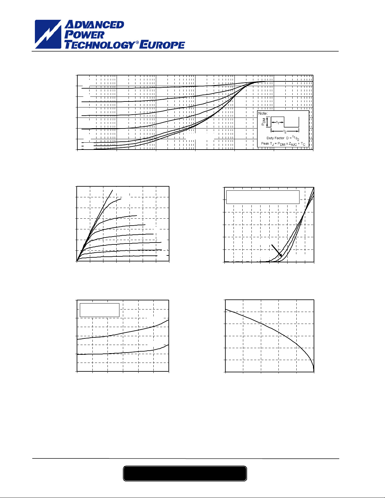
Typical Performance Curve
Maximum Effective Transient Thermal Impedance, Junction to Case vs Pulse Duration
0.35
0.9
0.3
APTM20TAM16FP
0.25
0.2
0.7
0.5
0.15
0.3
0.1
0.05
Thermal Impedance (°C/W)
0.1
0.05
0
Single Pulse
0.00001 0.0001 0.001 0.01 0.1 1 10
rectangular Pulse Duration (Seconds)
Low Voltage Output Characteristics Transfert Characteristics
350
300
VGS=15V
10V
250
200
150
100
, Drain Current (A)
D
I
50
0
0 4 8 12 16 20 24 28
V
, Drain to Source Voltage (V)
DS
9V
8.5 V
8V
7.5V
7V
6.5V
300
VDS > ID(on)xRDS(on)MAX
250µs pulse test @ < 0.5 duty cycle
250
200
150
100
, Drain Current (A)
D
I
50
TJ=25°C
TJ=125°C
0
0123 45678910
V
, Gate to Source Voltage (V)
GS
TJ=-55°C
R
vs Drain Current
DS(o n)
1.2
Normalized to
V
=10V @ 52A
GS
1.1
1
0.9
Drain to Source ON Resistance
0.8
0 25 50 75 100 125 150
DS(on)
R
, Drain Current (A)
I
D
VGS=10 V
VGS=20V
DC Drain Current vs Case Temperature
120
100
80
60
40
, DC Drain Current (A)
20
D
I
0
25 50 75 100 125 150
T
, Case Temperature (°C)
C
APT website – http://www.advancedpower.com 4
APTM20TAM16FP – Rev 0 September, 2004
6
Page 5

APTM20TAM16FP
–
g
(
)
, Drain to Source Breakdown
DSS
BV
(TH), Threshold Voltage
GS
V
Breakdown Voltage vs Temperature
1.15
1.10
1.05
Normalized
1.00
e
0.95
Volta
0.90
-50 -25 0 25 50 75 100 125 150
T
, Junction Temperature (°C)
J
Threshold Voltage vs Temperature
1.2
1.1
1.0
0.9
0.8
(Normalized)
0.7
0.6
-50 -25 0 25 50 75 100 125 150
T
, Case Temperature (°C)
C
ON resistance vs Temperature
2.5
VGS=10V
= 52A
I
D
2.0
1.5
1.0
(Normalized)
0.5
0.0
-50 -25 0 25 50 75 100 125 150
RDS(on), Drain to Source ON resistance
, Junction Temperature (°C)
T
J
Maximum Safe Operating Area
1000
limited by
R
DS on
100
10
, Drain Current (A)
D
I
Single pulse
T
=150°C
J
1
1 10 100 1000
, Drain to Source Voltage (V)
V
DS
100µs
1ms
10ms
100ms
Capacitance vs Drain to Source Voltage
100000
10000
Ciss
Coss
Gate Charge vs Gate to Source Voltage
14
ID=104A
12
T
=25°C
J
VDS=40V
VDS=100V
10
8
VDS=160V
6
1000
C, Capacitance (pF)
Crss
100
0 1020304050
, Drain to Source Voltage (V)
V
DS
4
2
, Gate to Source Voltage (V)
GS
V
0
0 20 40 60 80 100 120 140 160
Gate Charge (nC)
APT website – http://www.advancedpower.com 5
APTM20TAM16FP – Rev 0 September, 2004
6
Page 6

APTM20TAM16FP
–
t
Delay Times vs Current
120
100
(ns)
80
60
40
20
VDS=133V
=5Ω
R
G
T
=125°C
J
L=100µH
d(off)
and t
d(o n)
t
0
0 25 50 75 100 125 150 175
I
, Drain Current (A)
D
Switching Energy vs Current
2
VDS=133V
=5Ω
R
G
T
=125°C
1.5
J
(mJ)
off
L=100µH
1
and E
on
E
0.5
t
E
d(off)
t
off
d(on)
Rise and Fall times vs Current
160
VDS=133V
140
120
100
(ns)
f
and t
r
t
80
60
=5Ω
R
G
=125°C
T
J
L=100µH
t
f
t
r
40
20
0
0 25 50 75 100 125 150 175
, Drain Current (A)
I
D
Switching Energy vs Gate Resistance
3
VDS=133V
=104A
I
D
2.5
E
on
2
=125°C
T
J
L=100µH
1.5
1
Switching Energy (mJ)
E
off
E
on
0
0 25 50 75 100 125 150 175
, Drain Current (A)
I
D
Operating Frequency vs Drain Curren
300
250
200
VDS=133V
D=50%
=5Ω
R
G
=125°C
T
J
0.5
0 5 10 15 20 25 30 35 40 45 50
Gate Resistance (Ohms)
Source to Drain Diode Forward Voltage
1000
TJ=150°C
100
150
TJ=25°C
100
10
Frequency (kHz)
50
0
25 38 50 63 75 88 100
I
, Drain Current (A)
D
, Reverse Drain Current (A)
DR
I
1
0.2 0.4 0.6 0.8 1 1.2 1.4 1.6 1.8
V
, Source to Drain Voltage (V)
SD
APT re se rves the rig ht to c ha ng e , wi t ho ut no t ic e , the s pecificatio ns and i nfo rmatio n conta i ne d here in
APT's products are covered by one or more of U.S patents 4,895,810 5,045,903 5,089,434 5,182,234 5,019,522
5,262,336 6,503,786 5,256,583 4,748,103 5,283,202 5,231,474 5,434,095 5,528,058 and foreign patents. U.S and Foreign patents pending. All Rights Reserved.
APT website – http://www.advancedpower.com 6
APTM20TAM16FP – Rev 0 September, 2004
6
 Loading...