

www.DataSheet4U.com
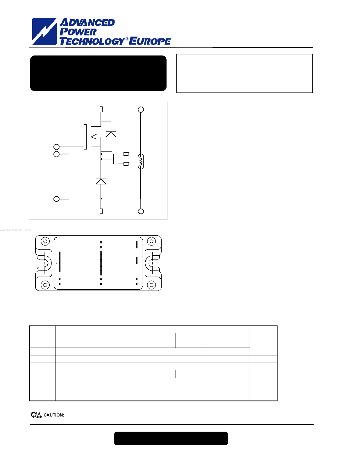
APTM20SKM08T
r
MOSFET Power Module
Buck chopper
VBUS
Q1
G1
S1
0/VBUS SENSE
0/VBUS
0/VB US
SENSE
VBUS
S1
G1
0/VB US
0/VB US
SENSE
OUT
NTC2
NT C1
OUT
OUT
NTC2
NTC1
Absolute maximum ratings
Symbol Parameter Max ratings Unit
V
Drain - Source Breakdown Voltage 200 V
DSS
ID Continuous Drain Current
IDM Pulsed Drain current 832
VGS Gate - Source Voltage ±30 V
R
Drain - Source ON Resistance 8
DSon
PD Maximum Power Dissipation Tc = 25°C 781 W
IAR Avalanche current (repetitive and non repetitive) 100 A
EAR Repetitive Avalanche Energy 50
EAS Single Pulse Avalanche Energy 3000
These Devices are sensitive to Electrostatic Discharge. Pr oper Handing Procedures Should Be Followed.
V
R
I
= 200V
DSS
DSon
= 208A @ Tc = 25°C
D
Application
· AC and DC motor control
· Switched Mode Power Supplies
Features
· Power MOS 7
- Low R
- Low input and Miller capacitance
- Low gate charge
- Avalanche energy rated
- Very rugged
· Kelvin source for easy drive
· Very low stray inductance
- Symmetrical design
- Lead frames for power connections
· Internal thermistor for temperature monitoring
· High level of integration
Benefits
· Outstanding performance at high frequency operation
· Direct mounting to heatsink (isolated package)
· Low junction to case thermal resistance
· Solderable terminals both for power and signal fo
easy PCB mounting
· Low profile
Tc= 25°C 208
= 80°C 155
T
c
= 8mW max @ Tj = 25°C
®
MOSFETs
DSon
A
mW
mJ
APT website –http://www.advancedpower.com
1–6
APTM20SKM08T – Rev 2 May, 2004
APTM20SKM08T
All ratings @ Tj = 25°C unless otherwise specified
Electrical Characteristics
Symbol Characteristic Test Conditions Min Typ Max Unit
BV
Drain - Source Breakdown Voltage VGS = 0V, ID = 375µA 200 V
DSS
I
Zero Gate Voltage Drain Current
DSS
R
Drain – Source on Resistance VGS = 10V, ID = 104A
DS(on)
V
Gate Threshold Voltage VGS = VDS, ID = 5mA 3 5 V
GS(th)
I
Gate – Source Leakage Current VGS = ±30 V, VDS = 0V ±150 nA
GSS
VGS = 0V,VDS = 200V T
VGS = 0V,VDS = 160V Tj = 125°C 750
Dynamic Characteristics
Symbol Characteristic Test Conditions Min Typ Max Unit
Input Capacitance 14.4
C
iss
C
Output Capacitance 4.66
oss
C
Reverse Transfer Capacitance
rss
Qg Total gate Charge 280
Qgs Gate – Source Charge 106
Qgd Gate – Drain Charge
T
Turn-on Delay Time 32
d(on)
T
Rise Time 64
r
T
Turn-off Delay Time 88
d(off)
T
Fall Time
f
E
Turn-on Switching Energy u 1698
on
E
Turn-off Switching Energy v
off
= 0V
V
GS
= 25V
V
DS
f = 1MHz
= 10V
V
GS
= 100V
V
Bus
= 208A
I
D
Inductive switching @ 125°C
V
= 15V
GS
= 133V
V
Bus
= 208A
I
D
= 2.5W
R
G
Inductive switching @ 25°C
V
= 15V, V
GS
= 208A, RG = 2.5Ω
I
D
= 133V
Bus
= 25°C 150
j
8
0.29
134
116
1858
µA
mW
nF
nC
ns
µJ
E
Turn-on Switching Energy u 1872
on
E
Turn-off Switching Energy v
off
Inductive switching @ 125°C
V
= 15V, V
GS
= 208A, RG = 2.5Ω
I
D
= 133V
Bus
µJ
1972
Diode ratings and characteristics
Symbol Characteristic Test Conditions Min Typ Max Unit
Maximum Average Forward Current 50% duty cycle Tc = 85°C 180 A
I
F(AV)
IF = 180A 1.1
VF Diode Forward Voltage
trr Reverse Recovery Time
Qrr Reverse Recovery Charge
IF = 360A
I
= 180A Tj = 125°C
F
= 180A
I
F
= 133V
V
R
di/dt = 600A/µs
I
= 180A
F
= 133V
V
R
di/dt = 600A/µs
Tj = 25°C 31
= 125°C 60
T
j
Tj = 25°C 180
T
= 125°C 750
j
1.4
0.9
V
ns
nC
u Eon includes diode reverse recovery.
v In accordance with JEDEC standard JESD24-1.
APT website –http://www.advancedpower.com
2–6
APTM20SKM08T – Rev 2 May, 2004

APTM20SKM08T
Thermal and package characteristics
Symbol Characteristic Min Typ Max Unit
R
Junction to Case
thJC
V
RMS Isolation Voltage, any terminal to case t =1 min, I isol<1mA, 50/60Hz
ISOL
Transistor
Diode 0.32
TJ Operating junction temperature range
T
Storage Temperature Range -40 125
STG
TC Operating Case Temperature -40 100
Torque Mounting torque To Heatsink M5 4.7 N.m
Wt Package Weight 160 g
Temperature sensor NTC
Symbol Characteristic Min Typ Max Unit
R
Resistance @ 25°C
25
B
T
25/85
= 298.16 K 4080 K
25
R
=
R
T
exp
25
é
æ
ç
B
ê
85/25
ç
25
è
ë
T: Thermistor temperature
ù
ö
11
÷
R
-
TT
: Thermistor value at T
T
ú
÷
ø
û
Package outline
0.16
°C/W
2500 V
-40 150
°C
68
kW
APT website –http://www.advancedpower.com
3–6
APTM20SKM08T – Rev 2 May, 2004

Typical Performance Curve
R
Maximum Effective Transient Thermal Impedance, Junction to Case vs Pulse Duration
0.18
Thermal Impedance (°C/W)
0.16
0.14
0.12
0.08
0.06
0.04
0.02
0.9
0.7
0.1
0.5
0.3
0.1
0.05
0
0.00001 0.0001 0.001 0.01 0.1 1 10
APTM20SKM08T
Single Pulse
rectangular Pulse Duration (Seconds)
Low Voltage Output Characteristics
700
600
500
VGS=15V
10V
9V
400
300
200
, Drain Current (A)
D
I
100
0
0 4 8 1216202428
, Drain to S ource Voltage (V)
V
DS
R
vs Drain Current
DS(on)
1.2
Normalized to
V
=10V @ 104A
GS
1.1
1
0.9
Drain to Source ON Resistance
0.8
0 50 100 150 200 250 300
DS(on)
, Drain Current (A)
I
D
8.5V
8V
VGS=10V
VGS=20V
7.5V
6.5V
7V
600
Transfert Characteristics
VDS > ID(on)xRDS(on)MAX
250µs pulse test @ < 0.5 duty cycle
500
400
300
, Drain Current (A)
D
I
200
100
TJ=25°C
TJ=125°C
TJ=-55°C
0
012345678910
, Gate to Source Voltage (V)
V
GS
DC Drain Current vs Case Temperature
250
200
150
100
50
, DC Drain Current (A)
D
I
0
25 50 75 100 125 150
T
, Case Temperature (°C)
C
APT website –http://www.advancedpower.com
4–6
APTM20SKM08T – Rev 2 May, 2004

APTM20SKM08T
g
(
)
, Drain to Source Breakdown
DSS
BV
(TH), Threshold Voltage
GS
V
Breakdown Voltage vs Temperature
1.15
1.10
1.05
Normalized
1.00
e
0.95
Volta
0.90
-50 -25 0 25 50 75 100 125 150
, Junction Temperature (°C)
T
J
Threshold Vol tage vs Temperature
1.2
1.1
1.0
0.9
0.8
(Normalized)
0.7
0.6
-50 -25 0 25 50 75 100 125 150
, Case Temperature (°C)
T
C
ON resistance vs Temperature
2.5
VGS=10V
= 104A
I
D
2.0
1.5
1.0
(Normalized)
0.5
0.0
-50 -25 0 25 50 75 100 125 150
RDS(on), Drain to Source ON resistance
, Junction Temperature (°C)
T
J
Maximum Safe Operating Area
1000
limited by
R
DSon
100
10
, Drain Current (A)
D
I
Single pulse
=150°C
T
J
1
1 10 100 1000
V
, Drain to Source Voltage (V)
DS
100µs
1ms
10ms
100ms
Capacitance vs Drain to Source Voltage
100000
10000
Ciss
Coss
Gate Charge vs Gate to Source Voltage
14
12
ID=208A
=25°C
T
J
VDS=40V
VDS=100V
10
8
VDS=160V
6
1000
C, Capacitance (pF)
Crss
100
0 1020304050
, Drain to S ource Voltage (V)
V
DS
4
2
, Gate to Source Voltage (V)
GS
V
0
0 40 80 120 160 200 240 280 320
Gate Charge (nC)
APT website –http://www.advancedpower.com
5–6
APTM20SKM08T – Rev 2 May, 2004

APTM20SKM08T
Delay Times vs Current
120
100
80
60
40
20
VDS=133V
=2.5Ω
R
G
=125°C
T
J
L=100µH
(ns)
d(off)
and t
d(on)
t
0
0 50 100 150 200 250 300 350
I
, Drain Current (A)
D
Switching Energy vs Current
4
VDS=133V
=2.5Ω
R
G
3
=125°C
T
J
(mJ)
off
and E
on
E
L=100µH
2
1
t
E
d(off)
off
t
d(on)
Rise and Fall times vs Current
160
VDS=133V
140
120
100
(ns)
f
and t
r
t
80
60
=2.5Ω
R
G
=125°C
T
J
L=100µH
t
f
t
r
40
20
0
0 50 100 150 200 250 300 350
I
, Drain Current (A)
D
Switching Energy vs Gate Resistance
6
VDS=133V
=208A
I
D
5
=125°C
T
J
E
on
L=100µH
4
3
2
Switching Energy (mJ)
E
off
E
on
0
0 50 100 150 200 250 300 350
, Drain Current (A)
I
D
Operating Frequency vs Drain Current
300
VDS=133V
250
200
D=50%
=2.5Ω
R
G
=125°C
T
J
150
100
1
0 5 10 15 20 25
Gate Resistance (Ohms)
Source to Drain Diode Forward Voltage
1000
TJ=150°C
100
TJ=25°C
10
Frequency (kHz)
50
0
25 50 75 100 125 150 175 200
, Drain Current (A)
I
D
, Reverse Drain Current (A)
DR
I
1
0.20.40.60.8 1 1.21.41.61.8
, Source to Drain Voltage (V)
V
SD
APT reserves the right to change, without notice, the specifications and information contained herein
APT's products are covered b y one or more of U.S patents 4,895,810 5,045,903 5,089, 434 5,182, 234 5,019,522
5,262,3 36 6,503,786 5,256,583 4,7 48,103 5,283,202 5, 231,474 5,434, 095 5,528,05 8 and f oreign p atents. U.S and Forei gn pate nts pendi ng. All Righ ts Reserved.
APT website –http://www.advancedpower.com
6–6
APTM20SKM08T – Rev 2 May, 2004
 Loading...