

Advanced Power Technology APTM 20 HM 16 FT Service Manual
www.DataSheet4U.com
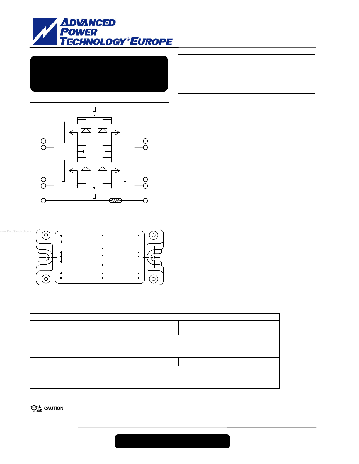
APTM20HM16FT
r
MOSFET Power Module
G1
S1
G2
S2
Full - Bridge
VBUS
Q1
OUT2OUT1
Q2
0/VBU SNTC1
G3
S3
VBUS
S1
G1
G4
S4
0/VB US
S2
G2
Q3
G3
S3
Q4
G4
S4
NTC2
OUT2
OUT1
NTC2
NTC1
Absolute maximum ratings
Symbol Parameter Max ratings Unit
V
Drain - Source Breakdown Voltage 200 V
DSS
ID Continuous Drain Current
IDM Pulsed Drain current 416
VGS Gate - Source Voltage ±30 V
R
Drain - Source ON Resistance 16
DSon
PD Maximum Power Dissipation Tc = 25°C 390 W
IAR Avalanche current (repetitive and non repetitive) 100 A
EAR Repetitive Avalanche Energy 50
EAS Single Pulse Avalanche Energy 3000
These Devices are sensitive to Electrostatic Discharge. Pr oper Handing Procedures Should Be Followed.
V
R
I
= 200V
DSS
= 16mW max @ Tj = 25°C
DSon
= 104A @ Tc = 25°C
D
Application
· Welding converters
· Switched Mode Power Supplies
· Uninterruptible Power Supplies
Features
· Power MOS 7
- Low R
®
FREDFETs
DSon
- Low input and Miller capacitance
- Low gate charge
- Fast intrinsic reverse diode
- Avalanche energy rated
- Very rugged
· Kelvin source for easy drive
· Very low stray inductance
- Symmetrical design
- Lead frames for power connections
· Internal thermistor for temperature monitoring
· High level of integration
Benefits
· Outstanding performance at high frequency operation
· Direct mounting to heatsink (isolated package)
· Low junction to case thermal resistance
· Solderable terminals both for power and signal fo
easy PCB mounting
· Low profile
Tc = 25°C 104
= 80°C 77
T
c
A
mW
mJ
APT website –http://www.advancedpower.com
1–6
APTM20HM16FT – Rev 1 May, 2004
APTM20HM16FT
All ratings @ Tj = 25°C unless otherwise specified
Electrical Characteristics
Symbol Characteristic Test Conditions Min Typ Max Unit
BV
Drain - Source Breakdown Voltage VGS = 0V, ID = 250µA 200 V
DSS
I
Zero Gate Voltage Drain Current
DSS
R
Drain – Source on Resistance VGS = 10V, ID = 52A
DS(on)
V
Gate Threshold Voltage VGS = VDS, ID = 2.5mA 3 5 V
GS(th)
I
Gate – Source Leakage Current VGS = ±30 V, VDS = 0V ±100 nA
GSS
VGS = 0V,VDS = 200V T
VGS = 0V,VDS = 160V T
Dynamic Characteristics
Symbol Characteristic Test Conditions Min Typ Max Unit
Input Capacitance 7220
C
iss
C
Output Capacitance 2330
oss
C
Reverse Transfer Capacitance
rss
Qg Total gate Charge 140
Qgs Gate – Source Charge 53
Qgd Gate – Drain Charge
T
Turn-on Delay Time 32
d(on)
T
Rise Time 64
r
T
Turn-off Delay Time 88
d(off)
T
Fall Time
f
E
Turn-on Switching Energy u 849
on
E
Turn-off Switching Energy v
off
= 0V
V
GS
= 25V
V
DS
f = 1MHz
= 10V
V
GS
= 100V
V
Bus
=104A
I
D
Inductive switching @ 125°C
V
= 15V
GS
= 133V
V
Bus
I
= 104A
D
= 5Ω
R
G
Inductive switching @ 25°C
V
= 15V, V
GS
= 104A, RG = 5Ω
I
D
= 133V
Bus
= 25°C 250
j
= 125°C 1000
j
16
146
67
116
929
µA
mW
pF
nC
ns
µJ
E
Turn-on Switching Energy u 936
on
E
Turn-off Switching Energy v
off
Inductive switching @ 125°C
V
= 15V, V
GS
= 104A, RG = 5Ω
I
D
= 133V
Bus
µJ
986
Source - Drain diode ratings and characteristics
Symbol Characteristic Test Conditions Min Typ Max Unit
Continuous Source current
IS
(Body diode)
Tc = 25°C 104
Tc = 80°C 77
A
VSD Diode Forward Voltage VGS = 0V, IS = - 104A 1.3 V
dv/dt Peak Diode Recovery w 5 V/ns
= - 104A
I
trr Reverse Recovery Time
Qrr Reverse Recovery Charge
S
= 133V
V
R
/dt = 100A/µs
di
S
= - 104A
I
S
= 133V
V
R
/dt = 100A/µs
di
S
Tj = 25°C 230
= 125°C 450
T
j
Tj = 25°C 0.9
= 125°C 3.4
T
j
ns
µC
u Eon includes diode reverse recovery.
v In accordance with JEDEC standard JESD24-1.
w dv/dt numbers reflect the limitations of the circuit rather than the device itself.
£ - 104A di/dt £ 700A/µs VR £ V
I
S
Tj £ 150°C
DSS
APT website –http://www.advancedpower.com
2–6
APTM20HM16FT – Rev 1 May, 2004
 Loading...