

www.DataSheet4U.com
APTM20DUM05T
1 - 3
power for
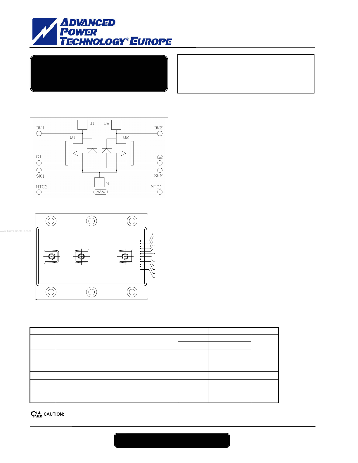
Dual common source
MOSFET Power Module
DK1
NC
1
G1
SK1
NC
SK2
G2
NC
D1
S
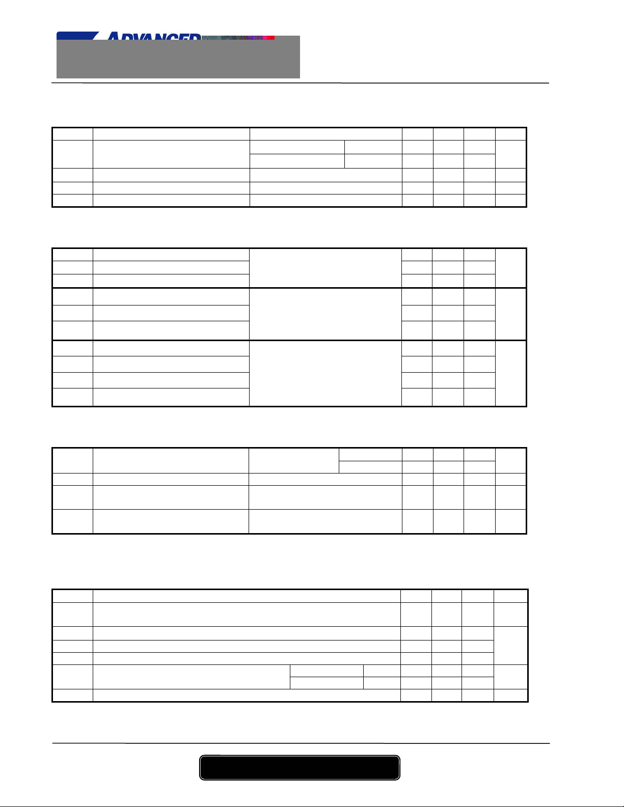
Absolute maximum ratings
Symbol Parameter Max ratings Unit
V
Drain - Source Breakdown Voltage 200 V
DSS
ID Continuous Drain Current
IDM Pulsed Drain current 700
VGS Gate - Source Voltage ±30 V
R
Drain - Source ON Resistance 5
DSon
PD Maximum Power Dissipation Tc = 25°C 1250 W
IAR Avalanche current (repetitive and non repetitive) 333 A
EAR Repetitive Avalanche Energy 30
EAS Single Pulse Avalanche Energy 1300
D2
DK2
NC
NTC1
NTC2
These Devices are sensitive to Electrostatic Discharge. Proper Handing Procedures Should Be Followed.
V
R
= 200V
DSS
= 5mΩΩΩΩ max @ Tj = 25°C
DSon
ID = 333A @ Tc = 25°C
Application
• AC Switches
• Switched Mode Power Supplies
• Uninterruptible Power Supplies
Features
• Power MOS V® MOSFETs
- Low R
- Low input and Miller capacitance
- Low gate charge
- Avalanche energy rated
Benefits
- Very rugged
• Kelvin source for easy drive
• Kelvin Drain for VDS monitoring
• Very low stray inductance
- Symmetrical design
- M5 power connectors
• Internal thermistor for temperature monitoring
• High level of integration
• Outstanding performance at high frequency operation
• Direct mounting to heatsink (isolated package)
• Low junction to case thermal resistance
• Solderable terminals for signal and M5 for
easy PCB mounting
Tc = 25°C 333
Tc = 80°C 249
DSon
A
mΩ
mJ
APT website – http://www.advancedpower.com
APTM20DUM05T – Rev 0 June, 2003
APTM20DUM05T
2 - 3
Electrical Characteristics All ratings @ Tj = 25°C unless otherwise specified
Symbol Characteristic Test Conditions Min Typ Max Unit
BV
Drain - Source Breakdown Voltage VGS = 0V, ID = 500µA 200 V
DSS
I
Zero Gate Voltage Drain Current
DSS
R
Drain – Source on Resistance VGS = 10V, ID = 166.5A
DS(on)
V
Gate Threshold Voltage VGS = VDS, ID = 8mA 2 4 V
GS(th)
I
Gate – Source Leakage Current VGS = ±30 V, VDS = 0V ±250 nA
GSS
VGS = 0V,VDS = 200V
VGS = 0V,VDS = 160V
Dynamic Characteristics
Symbol Characteristic Test Conditions Min Typ Max Unit
C
Input Capacitance 40.8
iss
C
Output Capacitance 9.1
oss
C
Reverse Transfer Capacitance
rss
Qg Total gate Charge 1184
Qgs Gate – Source Charge 376
Qgd Gate – Drain Charge
T
Turn-on Delay Time 15
d(on)
T
Rise Time 25
r
T
d(off)
T
Turn-off Delay Time 50
Fall Time
f
VGS = 0V
VDS = 25V
f = 1MHz
VGS = 10V
V
= 100V
Bus
ID = 333A
Resistive Switching
VGS = 15V
V
= 100V
Bus
ID = 333A
RG = 0.22 Ω
Source - Drain diode ratings and characteristics
Symbol Characteristic Test Conditions Min Typ Max Unit
(Body diode)
VSD Diode Forward Voltage VGS = 0V, IS = - 333A 1.3 V
= - 333A, VR = 100V
I
trr Reverse Recovery Time
Qrr Reverse Recovery Charge
S
diS/dt = 800A/µs
IS = - 333A, VR = 100V
diS/dt = 800A/µs
Thermal and package characteristics
Symbol Characteristic Min Typ Max Unit
R
Junction to Case
thJC
V
RMS Isolation Voltage, any terminal to case
ISOL
t =1 min, I isol<1mA, 50/60Hz
TJ Operating junction temperature range
T
Storage Temperature Range -40 125
STG
TC Operating Case Temperature -40 100
Torque Mounting torque
To heatsink M5 2 3.5
For terminals M5 2 3.5
Wt Package Weight 550 g
Tj = 25°C 300
Tj = 125°C 2000
5
3.1
600
10
Tc = 25°C 333 IS Continuous Source current
Tc = 80°C 249
160 ns
10.4 µC
0.1 °C/W
2500 V
-40 150
µA
mΩ
nF
nC
ns
A
°C
N.m
APT website – http://www.advancedpower.com
APTM20DUM05T – Rev 0 June, 2003

APTM20DUM05T
3 - 3
Temperature sensor NTC
Symbol Characteristic Min Typ Max Unit
R25 Resistance @ 25°C
B
T
25/85
= 298.16 K 4080 K
25
Package outline
R
=
R
T
exp
25
B
85/25
25
T: Thermistor temperature
11
−
RT: Thermistor value at T
TT
68
kΩ
Ra 3,2
APT reserves the right to change, without notice, the specifications and information contained herein
APT's products are covered by one or more of U.S patents 4,895,810 5,045,903 5,089,434 5,182,234 5,019,522
5,262,336 6,503,786 5,256,583 4,748,103 5,283,202 5,231,474 5,434,095 5,528,058 and foreign patents. U.S and Foreign patents pending. All Rights Reserved.
APT website – http://www.advancedpower.com
APTM20DUM05T – Rev 0 June, 2003
 Loading...