

www.DataSheet4U.com
APTM20DHM16T
r
Asymmetrical - Bridge
MOSFET Power Module
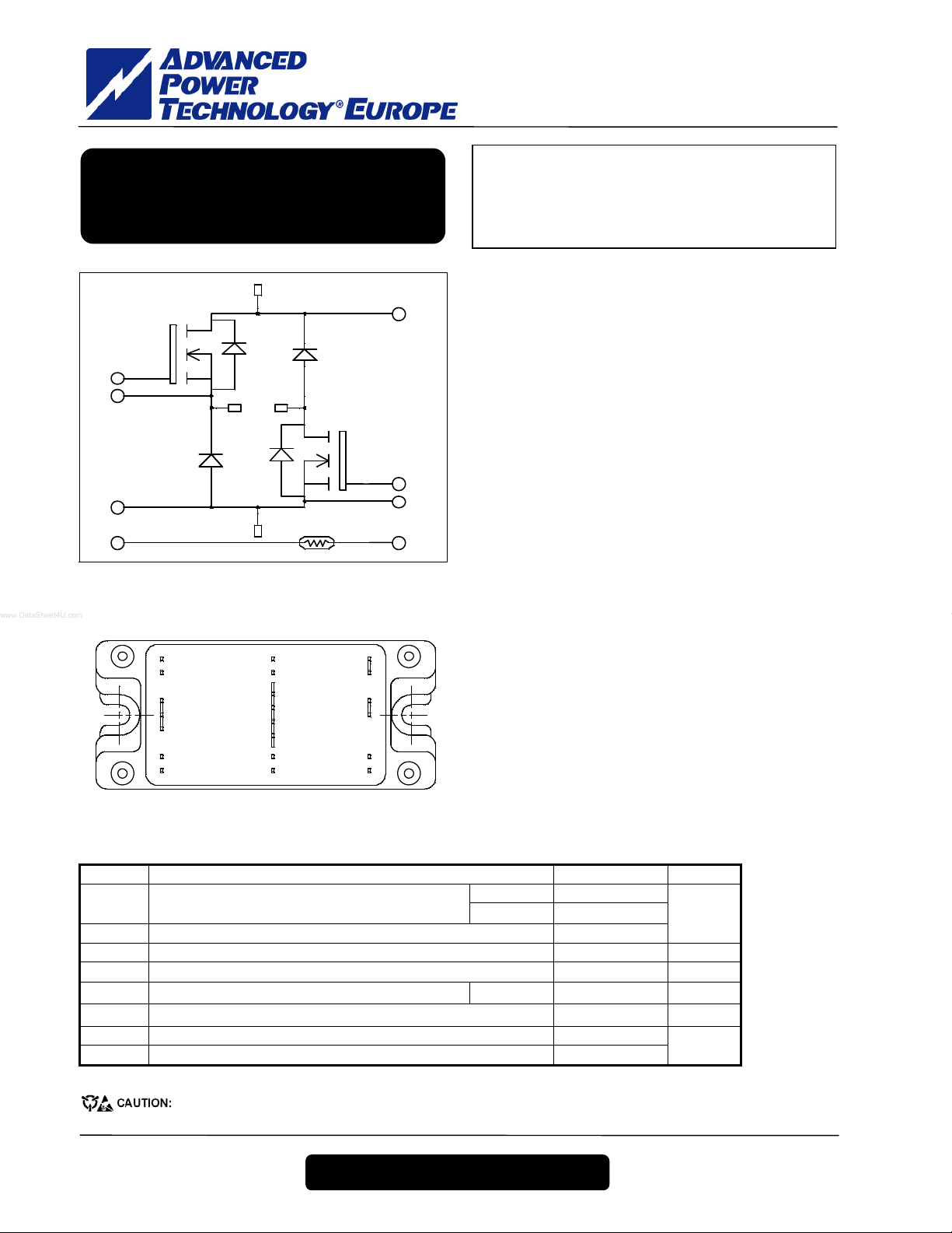
G1
S1
0/VBUS SENSE
NT C1
VBUS
Q1
CR3
OUT1 OUT2
Q4
CR2
0/VBUS
VB US SENS E
G4
S4
NTC2
VBUS
SENSE
VBUS
S1
G1
G4
S4
0/VB US
0/VB US
SENSE
OUT2
OUT1
NTC2
NTC1
Absolute maximum ratings
Symbol Parameter Max ratings Unit
Drain - Source Breakdown Voltage 200 V
V
DSS
ID Continuous Drain Current
IDM Pulsed Drain current 416
VGS Gate - Source Voltage ±30 V
R
Drain - Source ON Resistance 16
DSon
PD Maximum Power Dissipation Tc = 25°C 390 W
IAR Avalanche current (repetitive and non repetitive) 100 A
EAR Repetitive Avalanche Energy 50
EAS Single Pulse Avalanche Energy 3000
These Devices are sensitive to Electrostatic Discharge. Proper Handing Procedures Should Be Followed.
V
R
I
= 200V
DSS
= 16mW max @ Tj = 25°C
DSon
= 104A @ Tc = 25°C
D
Application
· Welding converters
· Switched Mode Power Supplies
· Switched Reluctance Motor Drives
Features
· Power MOS 7
- Low R
®
MOSFETs
DSon
- Low input and Miller capacitance
- Low gate charge
- Avalanche energy rated
- Very rugged
· Kelvin source for easy drive
· Very low stray inductance
- Symmetrical design
- Lead frames for power connections
· Internal thermistor for temperature monitoring
· High level of integration
Benefits
· Outstanding performance at high frequency operation
· Direct mounting to heatsink (isolated package)
· Low junction to case thermal resistance
· Solderable terminals both for power and signal fo
easy PCB mounting
· Low profile
Tc= 25°C 104
= 80°C 77
T
c
A
mW
mJ
APT website –http://www.advancedpower.com
1–6
APTM20DHM16T – Rev 2 May, 2004

APTM20DHM16T
All ratings @ Tj = 25°C unless otherwise specified
Electrical Characteristics
Symbol Characteristic Test Conditions Min Typ Max Unit
BV
Drain - Source Breakdown Voltage VGS = 0V, ID = 250µA 200 V
DSS
I
Zero Gate Voltage Drain Current
DSS
R
Drain – Source on Resistance VGS = 10V, ID = 52A
DS(on)
V
Gate Threshold Voltage VGS = VDS, ID = 2.5mA 3 5 V
GS(th)
I
Gate – Source Leakage Current VGS = ±30 V, VDS = 0V ±100 nA
GSS
VGS = 0V,VDS= 200V Tj = 25°C 100
VGS = 0V,VDS= 160V Tj = 125°C 500
16
Dynamic Characteristics
Symbol Characteristic Test Conditions Min Typ Max Unit
Input Capacitance 7220
C
iss
C
Output Capacitance 2330
oss
C
Reverse Transfer Capacitance
rss
Qg Total gate Charge 140
Qgs Gate – Source Charge 53
Qgd Gate – Drain Charge
T
Turn-on Delay Time 32
d(on)
T
Rise Time 64
r
T
Turn-off Delay Time 88
d(off)
T
Fall Time
f
E
Turn-on Switching Energy u 849
on
E
Turn-off Switching Energy v
off
= 0V
V
GS
= 25V
V
DS
f = 1MHz
= 10V
V
GS
= 100V
V
Bus
= 104A
I
D
Inductive switching @ 125°C
= 15V
V
GS
= 133V
V
Bus
I
= 104A
D
= 5W
R
G
Inductive switching @ 25°C
V
= 15V, V
GS
= 104A, RG = 5Ω
I
D
= 133V
Bus
146
67
116
929
µA
mW
pF
nC
ns
µJ
E
Turn-on Switching Energy u 936
on
E
Turn-off Switching Energy v
off
Inductive switching @ 125°C
V
= 15V, V
GS
= 104A, RG = 5Ω
I
D
= 133V
Bus
µJ
986
Diode ratings and characteristics
Symbol Characteristic Test Conditions Min Typ Max Unit
Maximum Average Forward Current
I
F(AV)
50% duty cycle Tc = 90°C
100 A
IF = 100A 1 1.1
VF Diode Forward Voltage
trr Reverse Recovery Time
Qrr Reverse Recovery Charge
IF = 200A 1.4
I
= 100A Tj = 125°C
F
= 100A
I
F
V
= 133V
R
di/dt = 200A/µs
I
= 100A
F
= 133V
V
R
di/dt = 200A/µs
Tj = 25°C 60
= 125°C 110
T
j
Tj = 25°C 200
= 125°C 840
T
j
0.9
V
ns
nC
u Eon includes diode reverse recovery.
v In accordance with JEDEC standard JESD24-1.
APT website –http://www.advancedpower.com
2–6
APTM20DHM16T – Rev 2 May, 2004

APTM20DHM16T
Thermal and package characteristics
Symbol Characteristic Min Typ Max Unit
R
Junction to Case
thJC
V
RMS Isolation Voltage, any terminal to case t =1 min, I isol<1mA, 50/60Hz
ISOL
Transistor
Diode 0.6
TJ Operating junction temperature range
T
Storage Temperature Range -40 125
STG
TC Operating Case Temperature -40 100
Torque Mounting torque To Heatsink M5 4.7 N.m
Wt Package Weight 160 g
Temperature sensor NTC
Symbol Characteristic Min Typ Max Unit
R
Resistance @ 25°C
25
B
T
25/85
= 298.16 K 4080 K
25
R
=
R
T
exp
25
é
æ
ç
B
ê
85/25
ç
25
è
ë
T: Thermistor temperature
ù
ö
11
÷
R
-
TT
: Thermistor value at T
T
ú
÷
ø
û
Package outline
0.32
°C/W
2500 V
-40 150
°C
68
kW
APT website –http://www.advancedpower.com
3–6
APTM20DHM16T – Rev 2 May, 2004

Typical Performance Curve
R
Maximum Effective Transient Thermal Impedance, Junction to Case vs Pulse Duration
0.35
0.9
0.3
0.25
0.15
0.05
Thermal Impedance (°C/W)
0.7
0.2
0.5
0.3
0.1
0.1
0.05
0
0.00001 0.0001 0.001 0.01 0.1 1 10
APTM20DHM16T
Single Pulse
rectangular Pulse Duration (Seconds)
Low Voltage Output Characteristics
350
300
250
VGS=15V
10V
9V
200
150
100
, Drain Current (A)
D
I
50
0
0 4 8 1216202428
, Drain to Source Voltage (V)
V
DS
R
vs Drain Current
DS(on)
1.2
Normalized to
V
=10V @ 52A
GS
1.1
1
0.9
Drain to Source ON Resistance
0.8
0 25 50 75 100 125 150
DS(on)
, Drain Current (A)
I
D
8.5V
8V
VGS=10V
VGS=20V
7.5V
6.5V
7V
300
Transfert Characteristics
VDS > ID(on)xRDS(on)MAX
250µs pulse test @ < 0.5 duty cycle
250
200
150
, Drain Current (A)
D
I
100
50
TJ=25°C
TJ=125°C
TJ=-55°C
0
012345678910
, Gate to Source Voltage (V)
V
GS
DC Drain Current vs Case Temperature
120
100
80
60
40
, DC Drain Current (A)
D
20
I
0
25 50 75 100 125 150
, Case Temperature (°C)
T
C
APT website –http://www.advancedpower.com
4–6
APTM20DHM16T – Rev 2 May, 2004

APTM20DHM16T
g
(
)
, Drain to Source Breakdown
DSS
BV
(TH), Threshold Voltage
GS
V
Breakdown Voltage vs Temperature
1.15
1.10
1.05
Normalized
1.00
e
0.95
Volta
0.90
-50 -25 0 25 50 75 100 125 150
, Junction Temperature (°C)
T
J
Threshold Voltage vs Temperature
1.2
1.1
1.0
0.9
0.8
(Normalized)
0.7
0.6
-50 -25 0 25 50 75 100 125 150
, Case Temperature (°C)
T
C
ON resistance vs Temperature
2.5
VGS=10V
= 52A
I
D
2.0
1.5
1.0
(Normalized)
0.5
0.0
-50 -25 0 25 50 75 100 125 150
RDS(on), Drain to Source ON resistance
, Junction Temperature (°C)
T
J
Maximum Safe Operating Area
1000
limited by
R
DSon
100
10
, Drain Current (A)
D
I
Single pulse
=150°C
T
J
1
1 10 100 1000
V
, Drain to Source Voltage (V)
DS
100µs
1ms
10ms
100ms
Capacitance vs Drain to Source Voltage
100000
10000
Ciss
Coss
Gate Charge vs Gate to Source Voltage
14
12
ID=104A
=25°C
T
J
VDS=40V
VDS=100V
10
8
VDS=160V
6
1000
C, Capacitance (pF)
Crss
100
0 1020304050
, Drain to Source Voltage (V)
V
DS
4
2
, Gate to Source Voltage (V)
GS
V
0
0 20406080100120140160
Gate Charge (nC)
APT website –http://www.advancedpower.com
5–6
APTM20DHM16T – Rev 2 May, 2004

APTM20DHM16T
Delay Times vs Current
120
100
t
(ns)
80
60
40
20
VDS=133V
=5Ω
R
G
=125°C
T
J
L=100µH
d(off)
and t
d(on)
t
0
0 255075100125150175
I
, Drain Current (A)
D
Switching Energy vs Current
2
(mJ)
off
and E
on
E
1.5
0.5
1
VDS=133V
=5Ω
R
G
=125°C
T
J
L=100µH
E
d(off)
off
t
d(on)
Rise and Fal l times vs Current
160
VDS=133V
140
120
100
(ns)
f
and t
r
t
80
60
=5Ω
R
G
=125°C
T
J
L=100µH
t
f
t
r
40
20
0
0 25 50 75 100 125 150 175
I
, Drain Current (A)
D
Switching Energy vs Gate Resistance
3
VDS=133V
=104A
I
D
2.5
E
on
2
=125°C
T
J
L=100µH
1.5
1
Switching Energy (mJ)
E
off
E
on
0
0 25 50 75 100 125 150 175
, Drain Current (A)
I
D
Operating Frequency vs Drain Current
300
VDS=133V
250
200
D=50%
=5Ω
R
G
=125°C
T
J
150
100
0.5
0 5 10 15 20 25 30 35 40 45 50
Gate Resistance (Ohms)
Source to Drain Diode Forward Voltage
1000
TJ=150°C
100
TJ=25°C
10
Frequency (kHz)
50
0
25 38 50 63 75 88 100
, Drain Current (A)
I
D
, Reverse Drain Current (A)
DR
I
1
0.20.40.60.8 1 1.21.41.61.8
, Sou rce to Drain Voltage (V)
V
SD
APT reserves the right to change, without notice, the specifications and information contained herein
APT's products are covered by one or more of U.S paten ts 4,895, 810 5,045, 903 5,089 ,434 5,18 2,234 5,019,522
5,262,3 36 6,503,786 5,256, 583 4,748,103 5,28 3,202 5,231,474 5,434,095 5,528,058 and forei gn pate nts. U .S and Foreign patents pending. All Rights Reserve d.
APT website –http://www.advancedpower.com
6–6
APTM20DHM16T – Rev 2 May, 2004
 Loading...