

www.DataSheet4U.com
APTM20DAM10T
r
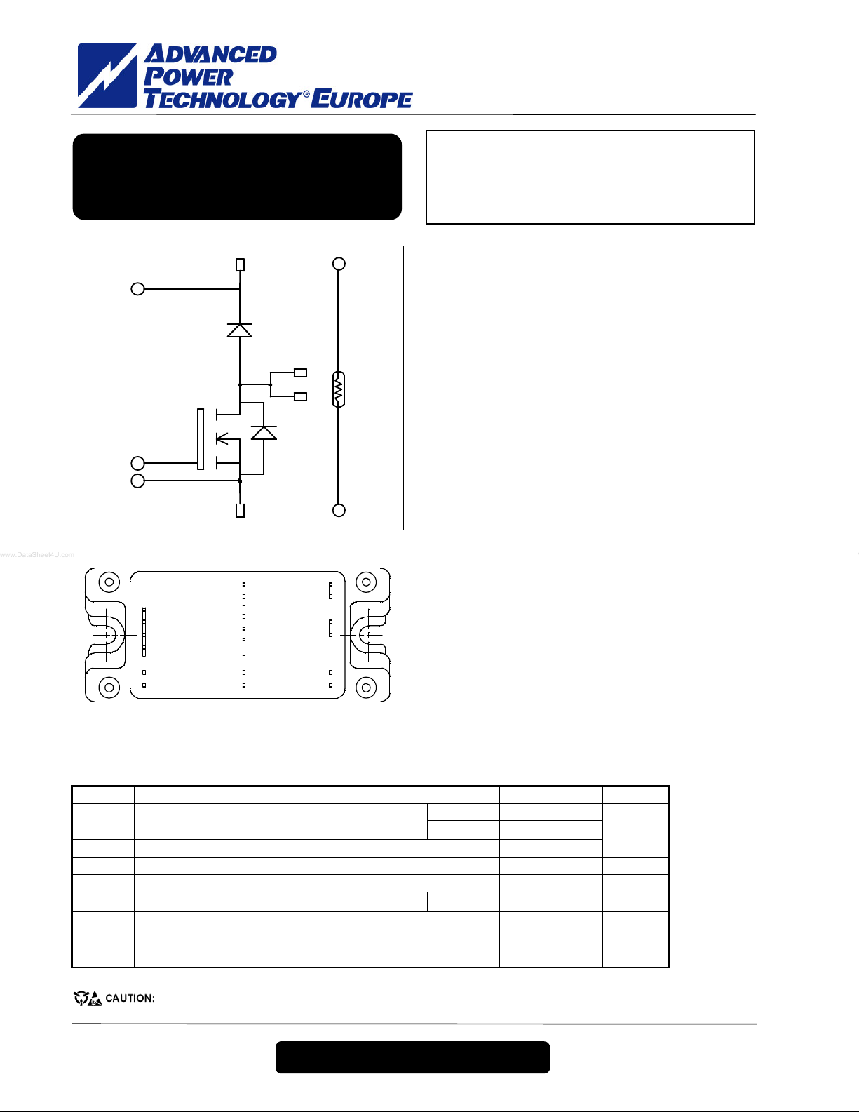
MOSFET Power Module
Boost chopper
VBUS SENSE
G2
S2
VBUS
VBUS
SENSE
Q2
0/VBUS
VBUS
CR1
G2
S2
0/VB US
S2
G2
NT C2
OUT
NT C1
OUT
OUT
NTC2
NTC1
Absolute maximum ratings
Symbol Parameter Max ratings Unit
V
Drain - Source Breakdown Voltage 200 V
DSS
ID Continuous Drain Current
IDM Pulsed Drain current 700
VGS Gate - Source Voltage ±30 V
R
Drain - Source ON Resistance 10
DSon
PD Maximum Power Dissipation Tc = 25°C 694 W
IAR Avalanche current (repetitive and non repetitive) 89 A
EAR Repetitive Avalanche Energy 50
EAS Single Pulse Avalanche Energy 2500
V
DSS
R
DSon
= 175A @ Tc = 25°C
I
D
Application
· AC and DC motor control
· Switched Mode Power Supplies
· Power Factor Correction
Features
· Power MOS 7
· Kelvin source for easy drive
· Very low stray inductance
· Internal thermistor for temperature monitoring
· High level of integration
Benefits
· Outstanding performance at high frequency operation
· Direct mounting to heatsink (isolated package)
· Low junction to case thermal resistance
· Solderable terminals both for power and signal fo
easy PCB mounting
· Low profile
Tc = 25°C 175
= 80°C 131
T
c
= 200V
= 10mW max @ Tj = 25°C
®
MOSFETs
- Low R
- Low input and Miller capacitance
- Low gate charge
- Avalanche energy rated
- Very rugged
- Symmetrical design
- Lead frames for power connections
DSon
A
mW
mJ
These Devices are sensitive to Electrostatic Discharge. Proper Handing Procedures Should Be Followed.
APT website –http://www.advancedpower.com
1–6
APTM20DAM10T – Rev 2 May, 2004

APTM20DAM10T
All ratings @ Tj = 25°C unless otherwise specified
Electrical Characteristics
Symbol Characteristic Test Conditions Min Typ Max Unit
BV
Drain - Source Breakdown Voltage VGS = 0V, ID = 375µA 200 V
DSS
I
Zero Gate Voltage Drain Current
DSS
R
Drain – Source on Resistance V
Gate Threshold Voltage VGS = VDS, ID = 5mA 3 5 V
Gate – Source Leakage Current VGS = ±30 V, VDS = 0V ±150 nA
GSS
V
DS(on)
GS(th)
I
VGS = 0V,VDS = 200V Tj = 25°C 150
VGS = 0V,VDS = 160V T
= 10V, ID = 87.5A 10
GS
= 125°C 750
j
Dynamic Characteristics
Symbol Characteristic Test Conditions Min Typ Max Unit
Input Capacitance 13.7
C
iss
C
Output Capacitance 4.36
oss
C
Reverse Transfer Capacitance
rss
Qg Total gate Charge 224
Qgs Gate – Source Charge 86
Qgd Gate – Drain Charge
T
Turn-on Delay Time 28
d(on)
T
Rise Time 56
r
T
Turn-off Delay Time 81
d(off)
T
Fall Time
f
E
Turn-on Switching Energy u 926
on
E
Turn-off Switching Energy v
off
= 0V
V
GS
= 25V
V
DS
f = 1MHz
= 10V
V
GS
= 100V
V
Bus
= 150A
I
D
Inductive switching @ 125°C
= 15V
V
GS
= 133V
V
Bus
I
= 150A
D
= 2.5W
R
G
Inductive switching @ 25°C
VGS = 15V, V
= 133V
Bus
ID = 150A, RG = 2.5Ω
0.19
94
99
910
µA
mW
nF
nC
ns
µJ
E
Turn-on Switching Energy u 1216
on
E
Turn-off Switching Energy v
off
Inductive switching @ 125°C
VGS = 15V, V
= 133V
Bus
ID = 150A, RG = 2.5Ω
µJ
1062
Diode ratings and characteristics
Symbol Characteristic Test Conditions Min Typ Max Unit
Maximum Average Forward Current 50% duty cycle
I
F(AV)
Tc = 85°C
120 A
IF = 120A 1.1 1.15
VF Diode Forward Voltage
trr Reverse Recovery Time
Qrr Reverse Recovery Charge
IF = 240A 1.4
I
= 120A Tj = 125°C
F
= 120A
I
F
V
= 133V
R
di/dt = 400A/µs
= 120A
I
F
= 133V
V
R
di/dt = 400A/µs
Tj = 25°C 31
= 125°C 60
T
j
Tj = 25°C 120
= 125°C 500
T
j
0.9
V
ns
nC
u Eon includes diode reverse recovery.
v In accordance with JEDEC standard JESD24-1.
APT website –http://www.advancedpower.com
2–6
APTM20DAM10T – Rev 2 May, 2004

APTM20DAM10T
Thermal and package characteristics
Symbol Characteristic Min Typ Max Unit
R
Junction to Case
thJC
V
RMS Isolation Voltage, any terminal to case t =1 min, I isol<1mA, 50/60Hz
ISOL
Transistor
Diode 0.46
TJ Operating junction temperature range
T
Storage Temperature Range -40 125
STG
TC Operating Case Temperature -40 100
Torque Mounting torque To Heatsink M5 4.7 N.m
Wt Package Weight 160 g
Temperature sensor NTC
Symbol Characteristic Min Typ Max Unit
R
Resistance @ 25°C
25
B
T
25/85
= 298.16 K 4080 K
25
R
=
R
T
exp
25
é
æ
ç
B
ê
85/25
ç
25
è
ë
T: Thermi stor temperature
ù
ö
11
÷
R
-
: Thermi stor value at T
T
ú
÷
TT
ø
û
Package outline
0.18
°C/W
2500 V
-40 150
°C
68
kW
APT website –http://www.advancedpower.com
3–6
APTM20DAM10T – Rev 2 May, 2004

Typical Performance Curve
R
Maximum E ffective Transient Thermal Impedance, Juncti on to Case vs Pulse Duration
0.2
Thermal Impedance (°C/W)
0.18
0.16
0.14
0.12
0.08
0.06
0.04
0.02
0.9
0.7
0.1
0.5
0.3
0.1
0.05
0
0.00001 0.0001 0.001 0.01 0.1 1 10
APTM20DAM10T
Single Pulse
rectangular Pulse Duration (Seconds)
Low Voltage Output Characteristics
500
VGS=15&10V
9V
400
300
200
, Drain Current (A)
D
100
I
0
0 5 10 15 20 25
, Drain to Source Voltage (V)
V
DS
RDS(on) vs Drain Current
1.2
Normalized to
V
1.15
=10V @ 87.5A
GS
1.1
1.05
1
0.95
0.9
(on) Drain to Source ON Resistance
0 40 80 120 160 200 240
DS
I
, Drain Current (A)
D
7.5V
7V
6.5V
5.5V
VGS=10V
VGS=20V
6V
400
Transfert Characteristics
VDS > ID(on)xRDS(on)MAX
250µs pulse test @ < 0.5 duty cycle
300
200
, Drain Current (A)
D
I
100
TJ=25°C
TJ=125°C
TJ=-55°C
0
23456789
V
, Gate to Source Voltage (V)
GS
DC Drain Current vs Case Temperature
200
180
160
140
120
100
80
60
40
, DC Drain Current (A)
D
I
20
0
25 50 75 100 125 150
, Case Temperature (°C)
T
C
APT website –http://www.advancedpower.com
4–6
APTM20DAM10T – Rev 2 May, 2004

APTM20DAM10T
g
(
)
, Drain to Source Breakdown
DSS
BV
(TH), Threshold Voltage
GS
V
Breakdown Voltage vs Temperature
1.2
1.1
1.0
Normalized
0.9
e
0.8
Volta
0.7
-50 -25 0 25 50 75 100 125 150
, Junction Temperature (°C)
T
J
Threshold Voltage vs Temperature
1.2
1.1
1.0
0.9
0.8
(Normalized)
0.7
0.6
-50 -25 0 25 50 75 100 125 150
, Case Temperature (°C)
T
C
ON resistance vs Temperature
2.5
VGS=10V
= 87.5A
I
D
2.0
1.5
1.0
(Normalized)
0.5
0.0
(on), Drain to Source ON resistance
DS
-50 -25 0 25 50 75 100 125 150
R
1000
T
, Junction Temperature (°C)
J
Maximum Safe Operating Area
limited by
R
DSon
100
10
, Drain Current (A)
D
I
Single pulse
T
=150°C
J
1
1 10 100 1000
VDS, Drain to Source Voltage (V)
100µs
1ms
10ms
DC line
Capacitance vs Drain to Source Voltage
100000
Ciss
10000
Coss
Gate Charge vs Gate to Source Voltage
12
VDS=40V
VDS=100V
VDS=160V
10
8
ID=150A
=25°C
T
J
6
1000
C, Capacitance (pF)
Crss
100
0 1020304050
V
, Drain to Source Voltage (V)
DS
4
2
, Gate to Source Voltage (V)
GS
V
0
0 50 100 150 200 250
Gate Charge (nC)
APT website –http://www.advancedpower.com
5–6
APTM20DAM10T – Rev 2 May, 2004

APTM20DAM10T
µ
µ
Delay Times vs Current
90
80
70
(ns)
and t
t
d(off)
d(on)
60
50
40
30
VDS=133V
=2.5Ω
R
G
=125°C
T
J
L=100
H
20
10
0 50 100 150 200 250 300
, Drain Current (A)
I
D
Switching Energy vs Current
2.5
(mJ)
off
and E
on
E
1.5
0.5
2
1
VDS=133V
=2.5Ω
R
G
=125°C
T
J
H
L=100
E
Rise and Fall times vs Current
160
VDS=133V
140
td
(off)
td
(on)
(ns)
f
and t
r
t
120
100
80
60
40
=2.5Ω
R
G
=125°C
T
J
L=100µH
t
f
t
r
20
0
0 50 100 150 200 250 300
I
, Drain Current (A)
D
Switching Energy vs Gate Resistance
3
2.5
2
VDS=133V
=150A
I
D
=125°C
T
J
L=100µH
E
off
E
on
on
E
off
1.5
Switching Energy (mJ)
0
0 50 100 150 200 250 300
ID, Drain Current (A)
Operating Frequency vs Drain Current
350
300
250
VDS=133V
D=50%
=2.5Ω
R
G
=125°C
T
J
200
1
0 5 10 15 20
Gate Resistance (Ohms)
Source to Drain Diode Forward Voltage
1000
100
TJ=150°C
TJ=25°C
150
100
Frequency (kHz)
50
0
20 40 60 80 100 120 140 160
I
, Drain Current (A)
D
10
, Reverse Drain Current (A)
DR
I
1
0.3 0.5 0.7 0.9 1.1 1.3 1.5 1. 7 1.9
, Sou rce to Drain Voltage (V)
V
SD
APT reserves the right to change, without notice, the specifications and information contained herein
APT's products are covered by one or more of U.S paten ts 4,89 5,810 5,045,903 5,089,434 5,182,23 4 5,019,522
5,262,3 36 6, 503, 786 5, 256,583 4 ,748,103 5,283,202 5,231, 474 5,434, 095 5,528 ,058 and f oreign pate nts. U .S and Foreign patents pendi ng. All Rights Reserve d.
APT website –http://www.advancedpower.com
6–6
APTM20DAM10T – Rev 2 May, 2004
 Loading...