

www.DataSheet4U.com
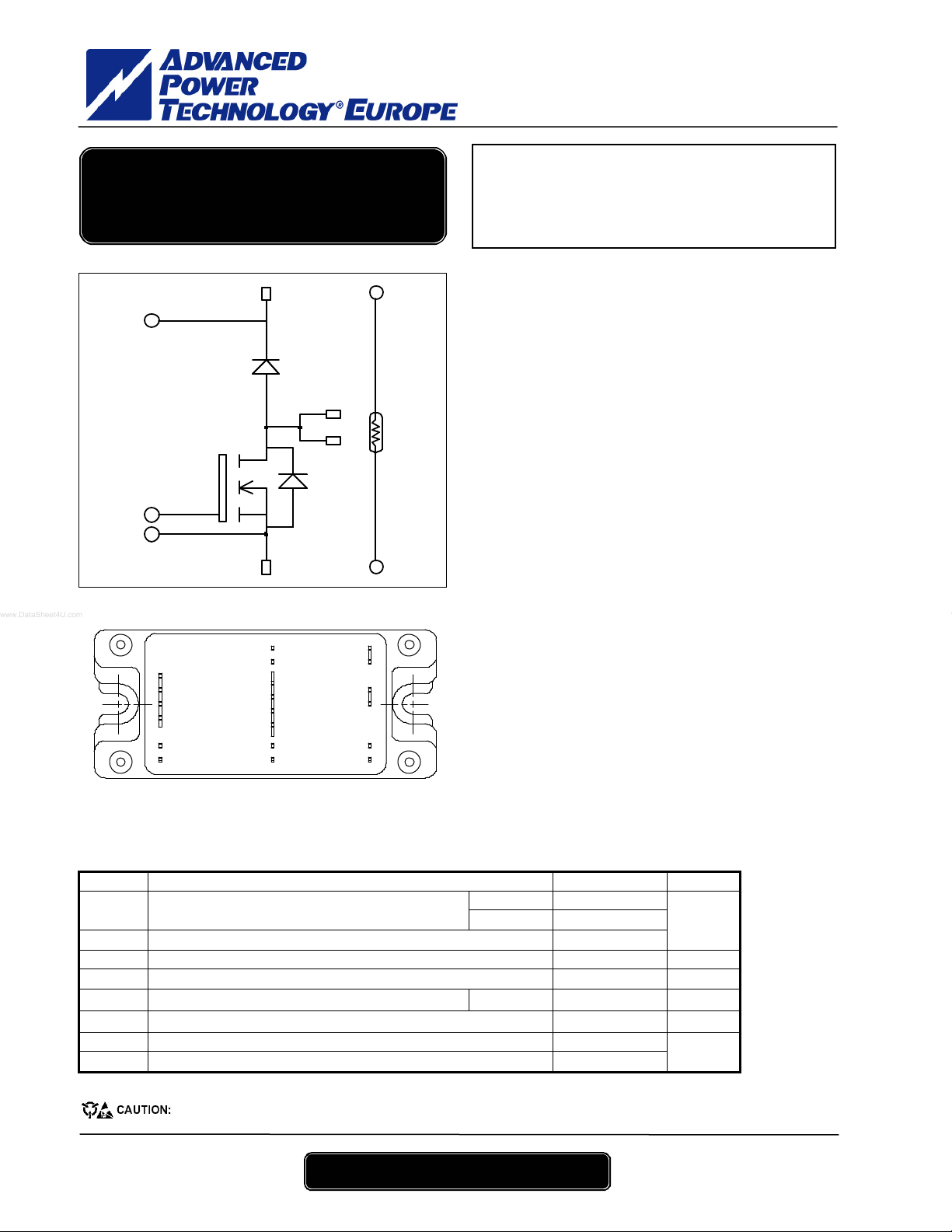
APTM20DAM08TG
–
S
B
G2
S2
oost chopper
VBUS
CR1
Q2
0/VBUS
G2
S2
VBUS
VBUS
SENSE
0/ VB US
S2
G2
NTC2
OUT
NTC1
OUT
OUT
NTC 2
NTC 1
MOSFET Power Module
VBUS SENSE
Absolute maximum ratings
ymbol Parameter Max ratings Unit
V
Drain - Source Breakdown Voltage 200 V
DSS
ID Continuo us Drain Current
IDM Pulsed Drain current 832
VGS Gate - Source Voltage ±30 V
R
Drain - Source ON Resistance 10
DSon
PD Maximum Power Dissipation Tc = 25°C 781 W
IAR Avalanche current (repetitive and non repetitive) 100 A
EAR Repetitive Avalanche Energy 50
EAS Single Pulse Avalanche Energy 3000
These Devices are sensitive to Electrostatic Discharge. Proper Handing Procedures Should Be Followed.
V
R
I
= 200V
DSS
= 8mΩ typ @ Tj = 25°C
DSon
= 208A @ Tc = 25°C
D
Application
• AC and DC motor control
• Switched Mode Power Supplies
• Power Factor Correction
Features
• Power MOS 7® MOSFETs
- Low R
- Low input and Miller capacitance
- Low gate charge
- Avalanche energy rated
- Very rugged
• Kelvin source for easy drive
• Very low stray inductance
- Symme trical design
- Lead frames for power connections
• Internal thermistor for temperature monitoring
• High level of integration
Benefits
• Outsta ndi ng performa nce at hi gh fr eq ue ncy ope r ati on
• Direct mounting to heatsink (isolated package)
• Low junction to case thermal resistance
• Solderable terminals both for power and signal for
easy PCB mounting
• Low profile
• RoHS compliant
Tc= 25°C 208
Tc = 80°C 155
DSon
A
mΩ
mJ
APT website – http://www.advancedpower.com 1
APTM20DAM08TG – Rev 3 November, 2005
6
APTM20DAM08TG
–
All ratings @ Tj = 25°C unless otherwise specified
Electrical Characteristics
Symbol Characteristic Test Conditions Min Typ Max Unit
I
Zero Gate Voltage Drain Current
DSS
R
Drain – Source on Resistance VGS = 10V, ID = 104A
DS(on)
V
Gate Threshold Voltage VGS = VDS, ID = 5mA 3 5 V
GS(th )
I
Gate – Source Leakage Current VGS = ±30 V, VDS = 0V ±150 nA
GS S
VGS = 0V,VDS = 200V T
VGS = 0V,VDS = 160V Tj = 125°C 750
Dynamic Characteristics
Symbol Characteristic Test Conditions Min Typ Max Unit
C
Input Capacitance 14.4
is s
C
Output Capacitance 4.66
oss
C
Reverse Transfer Capacitance
rss
Qg Total gate Charge 280
Qgs Gate – Source Charge 106
Qgd Gate – Drain C harge
T
Tur n-o n Del ay Ti me 32
d(on)
T
Rise Time 64
r
T
Turn-off Delay Time 88
d(off)
T
Fall Time
f
E
Turn-on Switching Energy 1698
on
E
Turn-off Switching Energy
off
VGS = 0V
VDS = 25V
f = 1MHz
VGS = 10V
V
= 100V
Bus
ID = 208A
Inductive switching @ 125°C
VGS = 15V
V
= 133V
Bus
ID = 208A
RG = 2.5Ω
Inductive switching @ 25°C
VGS = 15V, V
= 133V
Bus
ID = 208A, RG = 2.5Ω 1858
= 25°C 150
j
8 10
0.29
134
116
µA
mΩ
nF
nC
ns
µJ
E
Turn-on Switching Energy 1872
on
E
Turn-off Switching Energy
off
Inductive switching @ 125°C
VGS = 15V, V
= 133V
Bus
ID = 208A, RG = 2.5Ω
µJ
1972
Chopper diode ratings and characteristics
Symbol Characteristic Test Conditions Min Typ Max Unit
V
Maximum Peak Repetitive Reverse Voltage 200 V
RRM
IRM Maximum Reverse Leakage Current VR=200V
IF DC Forward Current Tc = 80°C 180 A
IF = 180A 1.1 1.15
IF = 360A 1.4 VF Diode Forward Voltage
IF = 180A Tj = 125°C
trr Reverse Recovery Time
IF = 180A
VR = 133V
Qrr Reverse Recovery Charge
di/dt = 600A/µs
Tj = 25°C 500
Tj = 125°C 750
0.9
Tj = 25°C 31
Tj = 125°C 60
Tj = 25°C 180
Tj = 125°C 750
µA
V
ns
nC
APT website – http://www.advancedpower.com 2
APTM20DAM08TG – Rev 3 November, 2005
6

APTM20DAM08TG
–
Thermal and package characteristics
Symbol Characteristic Min Typ Max Unit
R
Junction to Case Thermal Resistance
thJC
V
RMS Isolation Voltage, any terminal to case t =1 min, I isol<1mA, 50/60Hz 2500 V
ISOL
TJ Operating junction temperature range
T
Storage Temperature Range -40 125
STG
TC Operating Case Temperature -40 100
Torque Mounting torque To Heatsink M5 1.5 4.7 N.m
Wt Package Weight 160 g
Temperature sensor NTC
Symbol Characteristic Min Typ Max Unit
R25 Resistance @ 25°C 50
B
T
25/85
= 298.15 K 3952
25
(see application note APT0406 on www.advancedpower.com for more information).
R
=
R
T
exp
25
B
85/25
25
T: Thermis tor temperat ure
RT: Thermistor value at T
11
−
TT
SP4 Package outline (dimensions in mm)
Transistor 0.16
Diode 0.32
°C/W
-40 150
°C
kΩ
K
ALL DI MENSIO NS MARKE D " * " ARE T OL ERENCED AS :
APT website – http://www.advancedpower.com 3
APTM20DAM08TG – Rev 3 November, 2005
6

–
Typical Performance Curve
Maximum Effective Transient Thermal Impedance, Junction to Case vs Pulse Duration
0.18
0.16
0.9
0.14
0.12
0.08
0.06
0.04
Thermal Impedance (°C/W)
0.02
, Drain Current (A)
D
I
0.7
0.1
0.5
0.3
0.1
0.05
0
0.00001 0.0001 0.001 0.01 0.1 1 10
Low Voltage Output Characteristics Transfert Characteristics
1400
VGS=15V
1200
1000
800
600
400
200
0
0 4 8 1216202428
V
, Drain to Source Voltage (V)
DS
10V
Single Pulse
rectangular Pulse Duration (Seconds)
9V
8.5V
8V
7.5 V
7V
6.5V
APTM20DAM08TG
600
VDS > ID(on)xRDS(on)MAX
250µs pulse test @ < 0.5 duty cycle
500
400
300
200
, Drain Current (A)
D
I
100
0
0123 45678910
V
, Gate to Source Voltage (V)
GS
TJ=25°C
TJ=125°C
TJ=-55°C
DC Drain Current vs Case Temperature
250
200
1.2
1.1
R
DS(o n)
Normalized to
V
=10V @ 104A
GS
vs Drain Current
VGS=10 V
150
1
0.9
Drain to Source ON Resistance
0.8
0 50 100 150 200 250 300
DS(on)
R
, Drain Current (A)
I
D
VGS=20V
100
, DC Drain Current (A)
50
D
I
0
25 50 75 100 125 150
, Case Temperature (°C)
T
C
APT website – http://www.advancedpower.com 4
APTM20DAM08TG – Rev 3 November, 2005
6

APTM20DAM08TG
–
g
(
)
, Drain to Source Breakdown
DSS
BV
(TH), Threshold Voltage
GS
V
Breakdown Voltage vs Temperature
1.15
1.10
1.05
Normalized
1.00
e
0.95
Volta
0.90
-50 -25 0 25 50 75 100 125 150
T
, Junction Temperature (°C)
J
Threshold Voltage vs Temperature
1.2
1.1
1.0
0.9
0.8
(Normalized)
0.7
0.6
-50 -25 0 25 50 75 100 125 150
T
, Case Temperature (°C)
C
ON resistance vs Temperature
2.5
VGS=10V
= 104A
I
D
2.0
1.5
1.0
(Normalized)
0.5
0.0
-50 -25 0 25 50 75 100 125 150
RDS(on), Drain to Source ON resistance
, Junction Temperature (°C)
T
J
Maximum Safe Operating Area
1000
limited by
R
DS on
100
10
, Drain Current (A)
D
I
Single pulse
T
=150°C
J
1
1 10 100 1000
, Drain to Source Voltage (V)
V
DS
100µs
1ms
10ms
100ms
Capacitance vs Drain to Source Voltage
100000
10000
Ciss
Coss
Gate Charge vs Gate to Source Voltage
14
ID=208A
12
T
=25°C
J
VDS=40V
VDS=100V
10
8
VDS=160V
6
1000
C, Capacitance (pF)
Crss
100
0 1020304050
, Drain to Source Voltage (V)
V
DS
4
2
, Gate to Source Voltage (V)
GS
V
0
0 40 80 120 160 200 240 280 320
Gate Charge (nC)
APT website – http://www.advancedpower.com 5
APTM20DAM08TG – Rev 3 November, 2005
6

APTM20DAM08TG
–
t
Delay Times vs Current
120
100
80
60
40
20
VDS=133V
R
=2.5Ω
G
=125°C
T
J
L=100µH
(ns)
d(off)
and t
d(o n)
t
0
0 50 100 150 200 250 300 350
I
, Drain Current (A)
D
Switching Energy vs Current
4
VDS=133V
=2.5Ω
R
G
T
=125°C
3
J
2
1
L=100 µH
E
off
(mJ)
off
and E
on
E
0
0 5 0 100 1 50 20 0 250 3 00 3 50
, Drain Current (A)
I
D
t
d(off)
E
Rise and Fall times vs Current
160
VDS=133V
t
d(on)
140
120
100
(ns)
f
and t
r
t
80
60
=2.5Ω
R
G
=125°C
T
J
L=100µH
t
f
t
r
40
20
0
0 50 100 150 200 250 300 350
, Drain Current (A)
I
D
Switching Energy vs Gate Resistance
6
VDS=133V
=208A
off
E
on
Switching Energy (mJ)
5
4
3
2
I
D
=125°C
T
J
L=100 µH
E
off
E
on
1
0 5 10 15 20 25
Gate Resistance (Ohms)
Operating Frequency vs Drain Curren
350
300
250
200
VDS=133V
150
D=50%
=2.5Ω
R
G
100
Frequency (kHz)
50
=125°C
T
J
=75°C
T
C
Hard
switching
ZVS
ZCS
0
25 50 75 100 125 150 175 200
I
, Drain Current (A)
D
, Reverse Drain Current (A)
I
Source to Drain Diode Forward Voltage
1000
TJ=150°C
100
TJ=25°C
10
DR
1
0.2 0.4 0.6 0.8 1 1.2 1.4 1.6 1.8
V
, Source to Drain Voltage (V)
SD
APT re se rves the rig ht to c hange , wit ho ut no t ic e , the s pecificatio ns a nd i nfo rmatio n conta i ne d here in
APT's products are covered by one or more of U.S patents 4,895,810 5,045,903 5,089,434 5,182,234 5,019,522
5,262,336 6,503,786 5,256,583 4,748,103 5,283,202 5,231,474 5,434,095 5,528,058 and foreign patents. U.S and Foreign patents pending. All Rights Reserved.
APT website – http://www.advancedpower.com 6
APTM20DAM08TG – Rev 3 November, 2005
6
 Loading...