

www.DataSheet4U.com
APTM20AM10FT
–
S
P
MOSFET Power Module
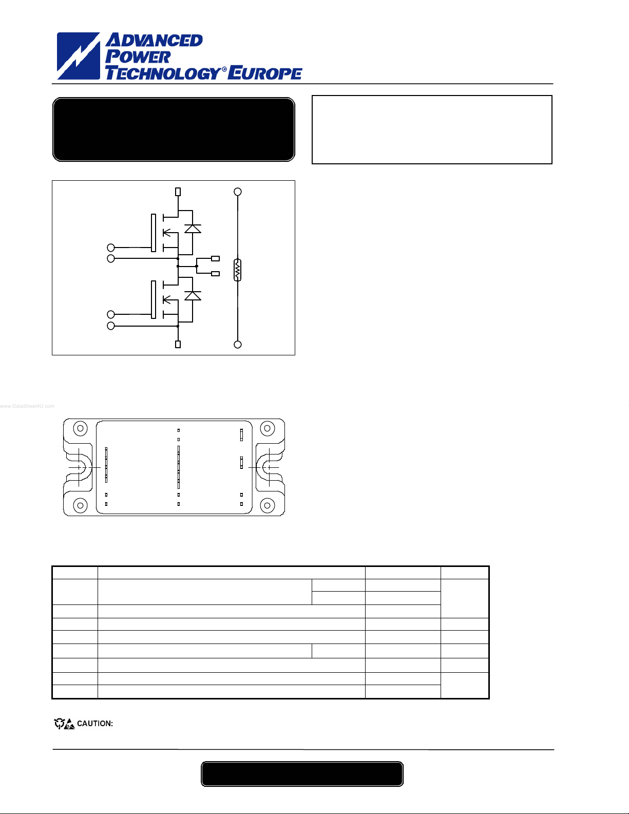
G1
S1
G2
S2
VBUS
S1 S2
G1
hase leg
VBUS
Q1
OUT
Q2
0/VBUS NT C1
G2
S2
0/VBUS
G2
NTC2
OUT
OUT
NTC2
NTC1
Absolute maximum ratings
ymbol Parameter Max ratings Unit
V
Drain - Source Breakdown Voltage 200 V
DSS
ID Continuo us Drain Current
IDM Pulsed Drain current 700
VGS Gate - Source Voltage ±30 V
R
Drain - Source ON Resistance 12
DSon
PD Maximum Power Dissipation Tc = 25°C 694 W
IAR Avalanche current (repetitive and non repetitive) 89 A
EAR Repetitive Avalanche Energy 50
EAS Single Pulse Avalanche Energy 2500
These Devices are sensitive to Electrostatic Discharge. Proper Handing Procedures Should Be Followed.
V
DSS
R
DSon
= 175A @ Tc = 25°C
I
D
Application
• Welding converters
• Switched Mode Power Supplies
• Uninterruptible Power Supplies
Features
• Power MOS 7® FREDFETs
- Low R
- Low input and Miller capacitance
- Low gate charge
- Fast intrinsic reverse diode
- Avalanche energy rated
- Very rugged
• Kelvin source for easy drive
• Very low stray inductance
- Symme trical design
- Lead frames for power connections
• Internal thermistor for temperature monitoring
• High level of integration
Benefits
• Outsta ndi ng performa nce at hi gh fr eq ue ncy oper ati on
• Direct mounting to heatsink (isolated package)
• Low junction to case thermal resistance
• Solderable terminals both for power a nd signal for
easy PCB mounting
• Low profile
Tc = 25°C 175
Tc = 80°C 131
= 200V
= 10mΩ typ @ Tj = 25°C
DSon
A
mΩ
mJ
APT website – http://www.advancedpower.com 1
APTM20AM10FT – Rev 2 July, 2005
6
APTM20AM10FT
–
All ratings @ Tj = 25°C unless otherwise specified
Electrical Characteristics
Symbol Characteristic Test Conditions Min Typ Max Unit
I
Zero Gate Voltage Drain Current
DSS
R
Drain – Source on Resistance VGS = 10V, ID = 87.5A
DS(on)
V
Gate Threshold Voltage VGS = VDS, ID = 5mA 3 5 V
GS(th )
I
Gate – Source Leakage Current VGS = ±30 V, VDS = 0V ±150 nA
GS S
VGS = 0V,VDS = 200V T
VGS = 0V,VDS = 160V T
Dynamic Characteristics
Symbol Characteristic Test Conditions Min Typ Max Unit
C
Input Capacitance 13.7
is s
C
Output Capacitance 4.36
oss
C
Reverse Transfer Capacitance
rss
Qg Total gate Charge 224
Qgs Gate – Source Charge 86
Qgd Gate – Drain C harge
T
Tur n-o n Delay Ti me 28
d(on)
T
Rise Time 56
r
T
Turn-off Delay Time 81
d(off)
T
Fall Time
f
E
Turn-on Switching Energy 926
on
E
Turn-off Switching Energy
off
VGS = 0V
VDS = 25V
f = 1MHz
VGS = 10V
V
= 100V
Bus
ID = 150A
Inductive switching @ 125°C
VGS = 15V
V
= 133V
Bus
ID = 150A
RG = 2.5Ω
Inductive switching @ 25°C
VGS = 15V, V
= 133V
Bus
ID = 150A, RG = 2.5Ω 910
= 25°C 375
j
= 125°C 1500
j
10 12
0.19
94
99
µA
mΩ
nF
nC
ns
µJ
E
Turn-on Switching Energy 1216
on
E
Turn-off Switching Energy
off
Inductive switching @ 125°C
VGS = 15V, V
= 133V
Bus
ID = 150A, RG = 2.5Ω
µJ
1062
Source - Drain diode ratings and characteristics
Symbol Characteristic Test Conditions Min Typ Max Unit
(Body diode)
VSD Diode Forward Voltage VGS = 0V, IS = - 150A 1.3 V
dv/dt Peak Diode Recovery X 8 V/ns
trr Reverse Recovery Time
IS = - 150A
VR = 133V
Qrr Reverse Recovery Charge
diS/dt = 200A/µs
X dv/dt numbers reflect the limitations of the circuit rather than the device itself.
IS ≤ - 150A di/dt ≤ 700A/µs VR ≤ V
Tj ≤ 150°C
DSS
Tc = 25°C 175 IS Continuo us Source current
Tc = 80°C 131
Tj = 25°C 220
Tj = 125°C 420
Tj = 25°C 2.14
Tj = 125°C 5.8
A
ns
µC
APT website – http://www.advancedpower.com 2
APTM20AM10FT – Rev 2 July, 2005
6

APTM20AM10FT
–
Thermal and package characteristics
Symbol Characteristic Min Typ Max Unit
R
Junction to Case 0.18 °C/W
thJC
V
RMS Isolation Voltage, any terminal to case t =1 min, I isol<1mA, 50/60Hz 2500 V
ISOL
TJ Operating junction temperature range
T
Storage Temperature Range -40 125
STG
TC Operating Case Temperature -40 100
Torque Mounting torque To Heatsink M5 1.5 4.7 N.m
Wt Package Weight 160 g
Temperature sensor NTC
Symbol Characteristic Min Typ Max Unit
R25 Resistance @ 25°C 50
B
T
25/85
= 298.15 K 3952
25
(see application note APT0406 on www.advancedpower.com for more information).
R
=
R
T
exp
25
B
85/25
25
T: Thermis tor temperature
RT: Thermistor value at T
11
−
TT
SP4 Package outline (dimensions in mm)
-40 150
°C
kΩ
K
APT website – http://www.advancedpower.com 3
APTM20AM10FT – Rev 2 July, 2005
6

–
Typical Performance Curve
Maximum Effective Transient Thermal Impedance, Junction to Case vs Pulse Duration
0.2
0.18
0.16
0.14
0.12
0.08
0.06
0.04
Thermal Impedance (°C/W)
0.02
0.9
0.7
0.1
0.5
0.3
0.1
0.05
0
0.00001 0.0001 0.001 0.01 0.1 1 10
APTM20AM10FT
Single Pulse
rectangular Pulse Duration (Seconds)
Low Voltage Output Characteristics
500
VGS=15&10V
9V
400
300
200
, Drain Current (A)
D
100
I
0
0 5 10 15 20 25
V
, Drain to Source Voltage (V)
DS
RDS(on) vs Drain Current
1.2
Normalized to
=10V @ 87.5A
V
1.15
GS
1.1
1.05
1
0.95
0.9
(on) Drain to Source ON Resistance
0 40 80 120 160 200 240
DS
R
I
, Drain Current (A)
D
7.5V
7V
6.5V
5.5V
VGS=10V
VGS=20V
400
Transfert Characteristics
VDS > ID(on)xRDS(on)MAX
250µs pulse test @ < 0.5 duty cycle
300
200
100
6V
, Drai n Current (A)
D
I
TJ=25°C
TJ=125°C
TJ=-55°C
0
2345 6789
V
, Gate to Source Voltage (V)
GS
DC Drain Current vs Case Temperature
200
180
160
140
120
100
80
60
40
, DC Dr ain Cu rrent (A)
D
I
20
0
25 50 75 100 125 150
T
, Case Temperature (°C)
C
APT website – http://www.advancedpower.com 4
APTM20AM10FT – Rev 2 July, 2005
6

APTM20AM10FT
–
g
(
)
, Drain to Source Breakdown
DSS
BV
(TH), Threshold Voltage
GS
V
Breakdown Voltage vs Temperature
1.2
1.1
1.0
Normalized
0.9
e
0.8
Volta
0.7
-50 -25 0 25 50 75 100 125 150
, Junction Temperature (°C)
T
J
Threshold Voltage vs Temperature
1.2
1.1
1.0
0.9
0.8
(Normalized)
0.7
0.6
-50 -25 0 25 50 75 100 125 150
T
, Case Temperature (°C)
C
ON resistance vs Temperature
2.5
VGS=10V
= 87.5A
I
D
2.0
1.5
1.0
(Normalized)
0.5
0.0
(on), Drain to Source ON resistance
DS
-50 -25 0 25 50 75 100 125 150
R
1000
, Junction Temperature (°C)
T
J
Maximum Safe Operating Area
limited by
R
DSon
100
10
, Drain Current (A)
D
I
Single pulse
=150°C
T
J
1
1 10 100 1000
VDS, Drain to Source Voltage (V)
100µs
1ms
10ms
DC line
Capacitance vs Drain to Source Voltage
100000
Ciss
10000
Coss
Gate Charge vs Gate to Source Voltage
12
VDS=40V
VDS=100V
VDS=160V
10
8
ID=150A
=25°C
T
J
6
1000
C, Capacitance (pF)
Crs s
100
0 1020304050
VDS, Drain to Source Voltage (V)
4
2
, Gate to Source Vol tage (V)
GS
V
0
0 50 100 150 200 250
Gate Charg e (n C)
APT website – http://www.advancedpower.com 5
APTM20AM10FT – Rev 2 July, 2005
6

APTM20AM10FT
–
µ
µ
t
Delay Times vs Current
90
80
70
(ns)
d(off)
and t
d(on)
t
60
50
40
30
VDS=133V
=2.5Ω
R
G
=125°C
T
J
L=100
H
20
10
0 50 100 150 200 250 300
ID, Drain Current (A)
Switching Energy vs Current
2.5
VDS=133V
=2.5Ω
R
G
2
T
=125°C
J
H
(mJ)
off
and E
on
E
L=100
1.5
1
0.5
Rise and Fall times vs Current
160
VDS=133V
140
td
(off)
td
(on)
120
100
(ns)
f
and t
r
t
80
60
40
20
=2.5Ω
R
G
=125°C
T
J
L=100µH
t
f
t
r
0
0 50 100 150 200 250 300
ID, Drain Current (A)
Switching Energy vs Gate Resistance
3
2.5
2
VDS=133V
=150A
I
D
=125°C
T
J
L=100µH
E
off
E
on
E
on
E
off
1.5
Switching Energy (mJ)
0
0 50 100 150 200 250 300
ID, Drain Current (A)
Operating Frequency vs Drain Curren
350
300
250
VDS=133V
D=50%
=2.5Ω
R
G
=125°C
T
J
200
1
0 5 10 15 20
Gate Resistance (Ohms)
Source to Drain Diode Forward Voltage
1000
100
TJ=150°C
TJ=25°C
150
100
Frequency (kHz)
50
0
20 40 60 80 100 120 140 160
I
, Drain Current (A)
D
10
, Reverse Drain Current (A)
DR
I
1
0.3 0.5 0.7 0.9 1.1 1.3 1.5 1.7 1.9
, Source to Drain Voltage (V)
V
SD
APT re se rves the rig ht to c hang e , wi t ho ut not ice , t he s pe cific atio ns and i nfo rmatio n conta ine d he re in
APT's products are covered by one or more of U.S patents 4,895,810 5,045,903 5,089,434 5,182,234 5,019,522
5,262,336 6,503,786 5,256,583 4,748,103 5,283,202 5,231,474 5,434,095 5,528,058 and foreign patents. U.S and Foreign patents pending. All Rights Reserved.
APT website – http://www.advancedpower.com 6
APTM20AM10FT – Rev 2 July, 2005
6
 Loading...