

www.DataSheet4U.com
–
r
–
S
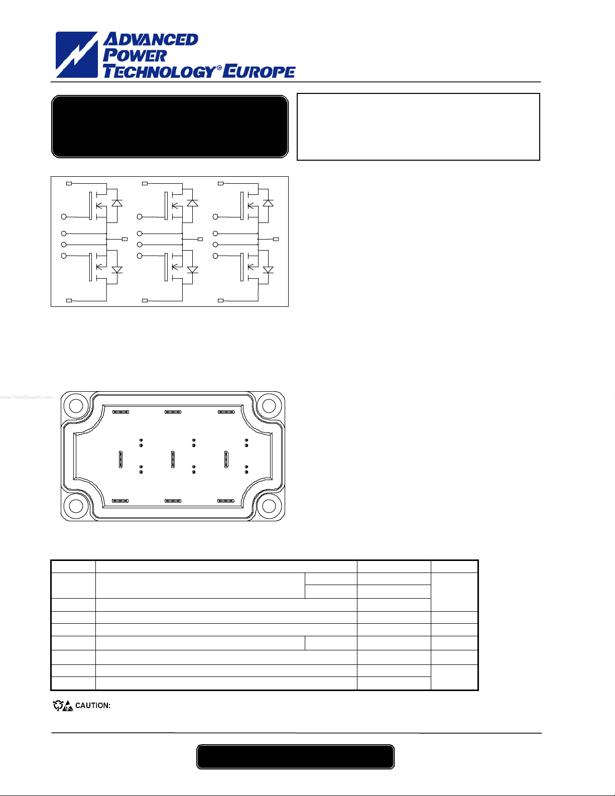
Triple dual common source
MOSFET Power Module
S1/S2
D3
G3
S3
S4
G4
D4
D1
G1
S1
S2
G2
D2
G1
S1
S3/S4
S2
G2
D 3 D 5
G3
S3
S4
G4
D 1
S1/S2
D 2
S3/S4
S5/S6
D5
G5
S5
S6
G6
D6
G5
S5
S6
G6
D 6D 4
S5/S6
V
R
I
D
Application
Features
Benefits
APTM120TDU57P
= 1200V
DSS
= 570mΩ max @ Tj = 25°C
DSon
= 17A @ Tc = 25°C
• AC Switches
• Switched Mode Power Supplies
• Uninterruptible Power Supplies
• Power MOS 7® MOSFETs
- Low R
- Low input and Miller capacitance
- Low gate c harge
- Avalanche energy rated
- Very rugged
• Kelvin source for easy drive
• Very low stray inductance
- Symme trical design
- Lead frames for power connections
• High level of integration
• Outstandi ng perfor mance at hi gh freque nc y ope ration
• Direct mounting to heatsink (isolated package)
• Low junction to case thermal resistance
• Solderable terminals both for power and signal for
easy PCB mounting
• Very low (12mm) profile
• Each leg can be easily paralleled to achieve a dual
commo n so urc e confi guratio n of three ti mes t he
current capability
DSon
Absolute maximum ratings
ymbol Parameter Max ratings Unit
V
Drain - Source Breakdown Voltage 1200 V
DSS
ID Conti nuous Drai n Current
Tc = 25°C 17
Tc = 80°C 13
IDM Pulsed Drain current 68
VGS Gate - Source Voltage ±30 V
R
Drain - Source ON Resistance 570
DSon
PD Maximum Power Dissipation Tc = 25°C 390 W
IAR Avalanche current (repetitive and non repetitive) 22 A
EAR Repetitive Avalanche Energy 50
EAS Single Pulse Avalanche Energy 3000
These Devices are sensitive to Electrostatic Discharge. Proper Handing Procedures S hould Be Followed.
APT website – http://www.advancedpower.com 1
A
mΩ
mJ
, 2004
Rev 0 Septembe
APTM120TDU57P
6
APTM120TDU57P
–
r
–
All ratings @ Tj = 25°C unless otherwise specified
Electrical Characteristics
Symbol Characteristic Test Conditions Min Typ Max Unit
BV
Drain - Source Breakdown Voltage VGS = 0V, ID = 250µA 1200 V
DSS
I
Zero Gate Voltage Drain Current
DSS
R
Drain – Source on Resistance VGS = 10V, ID = 8.5A
DS(on)
V
Gate Threshold Voltage VGS = VDS, ID = 2.5mA 3 5 V
GS(th )
I
Gate – Source Leakage Current VGS = ±30 V, VDS = 0V ±100 nA
GS S
Dynamic Characteristics
Symbol Characteristic Test Conditions Min Typ Max Unit
C
Input Capacitance 5155
is s
C
Output Capacitance 770
oss
C
Reverse Transfer Capacitance
rss
Qg Total gate Charge 187
Qgs Gate – Source Charge 24
Qgd Gate – Drain Charge
T
Tur n- o n Delay Ti me 20
d(on)
T
Rise Time 15
r
T
Turn-off Delay Time 160
d(off)
T
Fall Time
f
E
Tur n- o n Switchi ng E nergy X 990
on
E
Turn-off Switching Energy Y
off
VGS = 0V,VDS = 1200V Tj = 25°C 100
VGS = 0V,VDS = 1000V Tj = 125°C 500
570
µA
mΩ
VGS = 0V
VDS = 25V
f = 1MHz
130
pF
VGS = 10V
V
= 600V
Bus
ID = 17A
120
nC
Inductive switching @ 125°C
VGS = 15V
V
= 800V
Bus
ns
ID = 17A
RG = 5Ω
45
Inductive switching @ 25°C
VGS = 15V, V
= 800V
Bus
µJ
ID = 17A, RG = 5Ω 685
E
Tur n- o n Switchi ng E nergy X 1565
on
E
Turn-off Switching Energy Y
off
Inductive switching @ 125°C
VGS = 15V, V
= 800V
Bus
ID = 17A, RG = 5Ω
µJ
857
Source - Drain diode ratings and characteristics
Symbol Characteristic Test Conditions Min Typ Max Unit
(Body diode)
Tc = 25°C 17 IS Conti nuous Source c urrent
Tc = 80°C 13
A
VSD Diode Forward Voltage VGS = 0V, IS = - 17A 1.3 V
dv/dt Peak Diode Recovery Z 10 V/ns
trr Reverse Recovery Time Tj = 25°C 1291 ns
IS = - 17A
VR = 600V
Qrr Reverse Recovery Charge
X Eon includes diode reverse recovery.
diS/dt = 100A/µs
Tj = 25°C 29 µC
, 2004
Y In accordance with JEDEC standard JESD24-1.
Z dv/dt numbers reflect the li mitations of the circuit rather than the device itself.
IS ≤ - 17A di/dt ≤ 700A/µs VR ≤ V
Tj ≤ 150°C
DSS
Rev 0 Septembe
APT website – http://www.advancedpower.com 2
APTM120TDU57P
6

APTM120TDU57P
–
r
–
Thermal and package characteristics
Symbol Characteristic Min Typ Max Unit
R
Junction to Case IGBT 0.32 °C/W
thJC
V
RMS Isolation Voltage, any terminal to case t =1 min, I isol<1mA, 50/60Hz 2500 V
ISOL
TJ Operating junction temperature range -40 150
T
Storage Temperature Range -40 125
STG
TC Operating Case Temperature -40 100
Torque Mounting torque To heatsink M6 3 5 N.m
Wt Package Weight 250 g
Package outline
5 places (3:1)
°C
, 2004
Rev 0 Septembe
APT website – http://www.advancedpower.com 3
APTM120TDU57P
6

–
r
–
Typical Performance Curve
Maximum Effective Transient Thermal Impedance, Junction to Case vs Pulse Duration
0.35
0.3
0.9
APTM120TDU57P
0.25
0.2
0.7
0.5
0.15
0.1
0.05
Thermal Impedance (°C/W)
0.3
0.1
0.05
0
Single Pulse
0.00001 0.0001 0.001 0.01 0.1 1 10
rectangular Pulse Duration (Seconds)
Low Voltage Output Characteristics
50
VGS=15, 10 & 8V
40
30
7V
6.5V
80
70
60
50
Transfert Characteristics
VDS > ID(on)xRDS(on)MAX
250µs pulse test @ < 0.5 duty cycle
40
20
, Drain Curr ent (A)
D
10
I
0
0 5 10 15 20 25 30
, Drain to Source Voltage (V)
V
DS
6V
5.5 V
5V
30
20
, Drain Current (A)
D
I
10
TJ=25°C
TJ=125°C
TJ=-55° C
0
0123456789
V
, Gate to Source Voltage (V)
GS
DC Drain Current vs Case Temperature
20
16
12
1.4
1.3
1.2
R
DS(on)
Normalized to
V
=10V @ 8.5A
GS
vs Drain Current
VGS=10V
1.1
1
VGS=20V
0.9
0.8
0 10203040
(on) Drain to Source ON Resistance
DS
R
I
, Drain Current (A)
D
8
4
, DC Drain Current (A)
D
I
0
25 50 75 100 125 150
, Case Temperature (°C)
T
C
, 2004
Rev 0 Septembe
APT website – http://www.advancedpower.com 4
APTM120TDU57P
6

APTM120TDU57P
–
r
–
, Drain to Source Breakdown
DSS
BV
(TH), Threshold Voltage
GS
V
Breakdown Voltage vs Temperature
1.15
1.10
1.05
1.00
0.95
0.90
Voltage (Normalized)
0.85
-50 -25 0 25 50 75 100 125 150
T
, Junction Temperature (°C)
J
Threshold Voltage vs Temperature
1.2
1.1
1.0
0.9
0.8
(Normalized)
0.7
0.6
-50 -25 0 25 50 75 100 125 150
T
, Case Temperature (°C)
C
2.5
VGS=10V
=8.5A
I
D
2.0
1.5
1.0
(Normalized)
0.5
ON resistance vs Temperature
0.0
(on), Drain to Source ON resistance
DS
-50 -25 0 25 50 75 100 125 150
R
, Junction Temperature (°C)
T
J
Maximum Safe Operating Area
100
limited by RDSon
10
, Drain Current (A)
D
I
Single pulse
T
=150°C
J
1
1 10 100 1000
, Drain to Source Voltage (V)
V
DS
100µs
1ms
10m s
1200
Capacitance vs Drain to Source Voltage
100000
10000
1000
C, Capacitance (pF)
100
0 1020304050
, Drain to Source Voltage (V)
V
DS
Ciss
Coss
Crss
Gate Charge vs Gate to Source Voltage
14
12
10
ID=17A
T
=25°C
J
VDS=240V
VDS=600V
8
6
4
2
, Gate to Source Voltage (V)
GS
V
0
0 40 80 120 160 200 240
Gate Charge (nC )
VDS=960V
, 2004
Rev 0 Septembe
APT website – http://www.advancedpower.com 5
APTM120TDU57P
6

APTM120TDU57P
–
r
–
Delay Times vs Current
180
160
140
(ns)
120
100
80
60
40
VDS=800V
=5Ω
R
G
=125°C
T
J
L=100µH
d(off)
and t
d(on)
t
20
0
5 1015 20253035
, Drain Current (A)
I
D
Switching Energy vs Current
3
2.5
2
VDS=800V
=5Ω
R
G
=125°C
T
J
L=100µH
E
on
E
1.5
1
0.5
Switching Energy (mJ)
0
5 10152025 3035
ID, Drain Current (A)
t
off
d(on)
t
d(off)
80
Rise and Fall times vs Current
VDS=800V
=5Ω
R
G
=125°C
T
J
60
L=100µH
(ns)
f
40
and t
r
t
t
f
t
r
20
0
5 101520253035
, Drain Current (A)
I
D
Switching Energy vs Gate Resistance
4
3
2
VDS=800V
=17A
I
D
=125°C
T
J
L=100µH
E
off
E
on
1
Switching Energy (mJ)
0
0 5 10 15 20 25 30 35
Gate Resistance (Ohms)
Operating Frequency vs Drain Current
225
Source to Drain Diode Forward Voltage
1000
200
175
150
125
100
VDS=800V
D=50%
75
=5Ω
R
Frequency (kHz)
G
50
=125°C
T
J
25
=75°C
T
C
ZCS
ZVS
Hard
switching
0
4 6 8 10121416
, Drain Current (A)
I
D
100
TJ=150°C
10
, Reverse Drain Current (A)
DR
I
1
TJ=25°C
0.2 0.4 0.6 0.8 1 1.2 1.4 1.6 1.8
, Source to Drain Voltage (V)
V
SD
APT re s e rve s the rig ht to c hange, wit ho ut not ice, the spe cific atio ns an d informa tio n co nta i ne d he rein
APT's products are covered by one or more of U.S patents 4,895,810 5,045,903 5,089,434 5,182,234 5,019,522
5,262,336 6,503,786 5,256,583 4,748,103 5,283,202 5,231,474 5,434,095 5,528,058 and foreign patents. U.S and Foreign patents pending. All Rights Reserved.
, 2004
Rev 0 Septembe
APT website – http://www.advancedpower.com 6
APTM120TDU57P
6
 Loading...