

www.DataSheet4U.com
APTM120SK29T
–
–
S
B
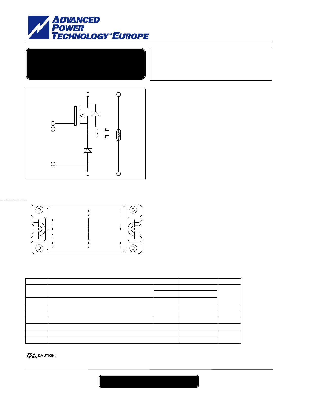
MOSFET Power Module
uck chopper
Q1
G1
S1
0/VBU S SENSE
0/VBUS
0/ VB US
SENSE
VBUS
S1
G1
0/ VB US
0/ VB US
SENSE
VBUS
OUT
NTC2
NTC1
OUT
OUT
NTC2
NTC1
Absolute maximum ratings
ymbol Parameter Max ratings Unit
V
Drain - Source Breakdown Voltage 1200 V
DSS
ID Continuo us Drain Curre nt
IDM Pulsed Drain current 136
VGS Gate - Source Voltage ±30 V
R
Drain - Source ON Resistance 290
DSon
PD Maximum Power Dissipation Tc = 25°C 780 W
IAR Avalanche current (repetitive and non repetitive) 22 A
EAR Repetitive Avalanche Energy 50
EAS Single Pulse Avalanche Energy 3000
These Devices are sensitive to Electrostatic Discharge. Proper Handing Procedures Should Be Followed.
V
R
I
= 1200V
DSS
= 290mΩ max @ Tj = 25°C
DSon
= 34A @ Tc = 25°C
D
Application
• AC and DC motor control
• Switched Mode Power Supplies
Features
• Power MOS 7® MOSFETs
- Low R
- Low input and Miller capacitance
- Low gate char ge
- Avalanche energy rated
- Very rugged
• Kelvin source for easy drive
• Very low stray inductance
- Symme trical design
- Lead frames for power connections
• Internal thermistor for temperature monitoring
• High level of integration
Benefits
• Outsta ndi ng performa nce at hi gh freq ue nc y operation
• Direct mounting to heatsink (isolated package)
• Low junction to case thermal resistance
• Solderable terminals both for power and signal for
easy PCB mounting
• Low profile
Tc = 25°C 34
Tc = 80°C 25
DSon
A
mΩ
mJ
Rev 0 July, 2004
APT website – http://www.advancedpower.com 1
APTM120SK29T
6
APTM120SK29T
–
–
All ratings @ Tj = 25°C unless otherwise specified
Electrical Characteristics
Symbol Characteristic Test Conditions Min Typ Max Unit
BV
Drain - Source Breakdown Voltage VGS = 0V, ID = 500µA 1200 V
DSS
I
Zero Gate Voltage Drain Current
DSS
R
Drain – Source on Resistance VGS = 10V, ID = 17A
DS(on)
V
Gate Threshold Voltage VGS = VDS, ID = 5mA 3 5 V
GS(th )
I
Gate – Source Leakage Current VGS = ±30 V, VDS = 0V ±150 nA
GS S
Dynamic Characteristics
Symbol Characteristic Test Conditions Min Typ Max Unit
C
Input Capacitance 10.3
is s
C
Output Capacitance 1.54
oss
C
Reverse Transfer Capacitance
rss
Qg Total gate Charge 374
Qgs Gate – Source Charge 48
Qgd Gate – Drain Charge
T
Tur n-on Del a y Ti me 20
d(on)
T
Rise Time 15
r
T
Turn-off Delay Time 160
d(off)
T
Fall Time
f
E
Tur n-on Sw itchi ng Energy X 1980
on
E
Turn-off Switching Energy Y
off
VGS = 0V,VDS = 1200V Tj = 25°C 200
VGS = 0V,VDS = 1000V Tj = 125°C 1000
290
µA
mΩ
VGS = 0V
VDS = 25V
f = 1MHz
0.26
nF
VGS = 10V
V
= 600V
Bus
ID = 34A
240
nC
Inductive switching @ 125°C
VGS = 15V
V
= 800V
Bus
ns
ID = 34A
RG = 2.5Ω
45
Inductive switching @ 25°C
VGS = 15V, V
= 800V
Bus
µJ
ID = 34A, RG = 2.5Ω 1371
E
Tur n-on Sw itchi ng Energy X 3131
on
E
Turn-off Switching Energy Y
off
Inductive switching @ 125°C
VGS = 15V, V
= 800V
Bus
ID = 34A, RG = 2.5Ω
µJ
1714
Diode ratings and characteristics
Symbol Characteristic Test Conditions Min Typ Max Unit
I
Maximum Average Forward Current 50% duty cycle Tc = 70°C 60 A
F(A V)
IF = 60A 2 2.5
trr Reverse Recovery Time
Qrr Reverse Recovery Charge
IF = 120A 2.3 VF Diode Forward Voltage
IF = 60A Tj = 125°C
IF = 60A
Tj = 25°C 400
VR = 800V
di/dt = 200A/µs
IF = 60A
Tj = 125°C 470
Tj = 25°C 1200
VR = 800V
di/dt = 200A/µs
Tj = 125°C 4000
1.8
V
ns
nC
X Eon includes diode reverse recovery.
Y In accordance with JEDEC standard JESD24-1.
Rev 0 July, 2004
APT website – http://www.advancedpower.com 2
APTM120SK29T
6
APTM120SK29T
–
–
Thermal and package characteristics
Symbol Characteristic Min Typ Max Unit
R
Junctio n to Case
thJC
V
RMS Isolation Voltage, any terminal to case t =1 min, I isol<1mA, 50/60Hz
ISOL
TJ Operating j unction temperature range
T
Storage Temperature Range -40 125
STG
TC Operating Case Temperature -40 100
Torque Mounting torque To Heatsink M5 4.7 N.m
Wt Package Weight 160 g
Temperature sensor NTC
Symbol Characteristic Min Typ Max Unit
R25 Resistance @ 25°C
B
T
25/85
= 298.16 K 4080 K
25
R
=
R
T
exp
25
B
85/25
25
T: Thermis tor temperat ure
11
−
RT: Thermistor value at T
TT
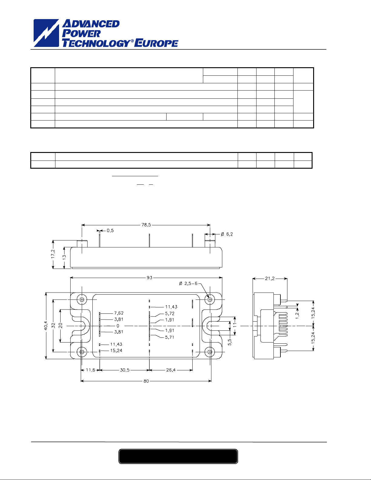
Package outline
Transistor 0.16
Diode 1.2
°C/W
2500 V
-40 150
°C
68
kΩ
Rev 0 July, 2004
APT website – http://www.advancedpower.com 3
APTM120SK29T
6

–
–
Typical Performance Curve
Maximum Effective Transient Thermal Impedance, Junction to Case vs Pulse Duration
0.18
0.16
0.14
0.12
0.1
0.08
0.06
0.04
0.02
Thermal Impedance (°C/W)
0.9
0.7
0.5
0.3
0.1
0.05
0
0.00001 0.0001 0.001 0.01 0.1 1 10
APTM120SK29T
Single Pulse
rectangular Pulse Duration (Seconds)
Low Voltage Output Characteristics
100
VGS=15, 10 & 8V
80
7V
60
40
, Drain Curr ent (A)
D
20
I
5.5V
0
0 5 10 15 20 25 30
, Drain to Source Voltage (V)
V
DS
R
vs Drain Current
1.4
1.3
1.2
DS(on)
Normalized to
V
=10V @ 17A
GS
VGS=10V
1.1
1
VGS=20V
0.9
0.8
0 20406080
(on) Drain to Source ON Resistance
DS
R
I
, Drain Current (A)
D
6.5 V
6V
5V
Transfert Characteristics
160
VDS > ID(on)xRDS(on)MAX
140
250µs pulse test @ < 0.5 duty cycle
120
100
80
60
40
, Drain Current (A)
D
I
20
TJ=25°C
TJ=125°C
TJ=-55°C
0
0123456789
V
, Gate to Source Voltage (V)
GS
DC Drain Current vs Case Temperature
40
30
20
10
, DC Drain Current (A)
D
I
0
25 50 75 100 125 150
, Case Temperature (°C)
T
C
Rev 0 July, 2004
APT website – http://www.advancedpower.com 4
APTM120SK29T
6

APTM120SK29T
–
–
, Drain to Source Breakdown
DSS
BV
(TH), Threshold Voltage
GS
V
Breakdown Voltage vs Tem perature
1.15
1.10
1.05
1.00
0.95
0.90
Voltage (Normalized)
0.85
-50 -25 0 25 50 75 100 125 150
T
, Junction Temperature (°C)
J
Threshold Voltage vs Temperature
1.2
1.1
1.0
0.9
0.8
(Normalized)
0.7
0.6
-50 -25 0 25 50 75 100 125 150
T
, Case Temperature (°C)
C
2.5
VGS=10V
=17A
I
D
2.0
1.5
1.0
(Normalized)
0.5
ON resistance vs Temperature
0.0
(on), Drain to Source ON resistance
DS
-50 -25 0 25 50 75 100 125 150
R
, Junction Temperature (°C)
T
J
Maximum Safe Operating Area
1000
100
limited by RDSon
10
, Drain Current (A)
D
I
Single pulse
T
=150°C
J
1
1 10 100 1000
, Drain to Source Voltage (V)
V
DS
100µs
1ms
10m s
1200
Capacitance vs Drain to Source Voltage
100000
10000
1000
C, Capacitance (pF)
100
0 1020304050
, Drain to Source Voltage (V)
V
DS
Ciss
Coss
Crss
Gate Charge vs Gate to Source Voltage
14
12
10
ID=34A
T
=25°C
J
VDS=240V
VDS=600V
8
6
4
2
, Gate to Source Voltage (V)
GS
V
0
0 80 160 240 320 400 480
Gate Charge (nC)
VDS=960V
Rev 0 July, 2004
APT website – http://www.advancedpower.com 5
APTM120SK29T
6

APTM120SK29T
–
–
Delay Times vs Current
180
150
(ns)
120
90
60
VDS=800V
=2.5Ω
R
G
=125°C
T
J
L=100µH
d(off)
and t
d(on)
t
30
0
10 20 30 40 50 60 70
I
, Drain Current (A)
D
Switching Energy vs Current
6
5
4
VDS=800V
=2.5Ω
R
G
=125°C
T
J
L=100 µH
E
3
2
1
Switching Energy (mJ)
0
10 20 30 40 50 60 70
I
, Drain Current (A)
D
80
Rise and Fall times vs Current
VDS=800V
=2.5Ω
R
G
=125°C
T
J
60
L=100µH
(ns)
f
40
and t
r
t
t
f
t
r
20
t
d(on)
t
d(off)
0
10 20 30 40 50 60 70
, Drain Current (A)
I
D
Switching Energy vs Gate Resistance
7
VDS=800V
=34A
I
on
E
off
6
D
=125°C
T
J
5
L=100µH
4
E
off
E
on
3
2
Switching Energy (mJ)
1
0.0 2.5 5.0 7.5 10.0 12.5 15.0 17.5
Gate Resistance (Ohms)
Operating Frequency vs Drain Current
225
Source to Drain Diode Forward Voltage
1000
200
=2.5Ω
G
=125°C
J
=75°C
C
ZCS
Hard
switching
, Drain Current (A)
I
D
ZVS
100
TJ=150°C
TJ=25°C
10
, Reverse Drain Current (A)
DR
I
1
0.2 0.4 0.6 0.8 1 1.2 1.4 1.6 1.8
, Source to Drain Voltage (V)
V
SD
175
150
125
100
VDS=800V
D=50%
75
R
Frequency (kHz)
50
T
25
T
0
8 121620242832
APT re se rves the rig ht to cha nge, witho ut not ice , t he s pe c ifica tio ns and i nfo rmatio n co nta ine d he re in
APT's products are covered by one or more of U.S patents 4,895,810 5, 045,903 5,089,434 5, 182,234 5,019,522
5,262,336 6,503,786 5,256,583 4,748,103 5,283,202 5,231,474 5,434,095 5,528,058 and foreign patents. U.S and Foreign patents pending. All Rights Reserved.
Rev 0 July, 2004
APT website – http://www.advancedpower.com 6
APTM120SK29T
6
 Loading...