

www.DataSheet4U.com
APTM120H57FT3
–
r
–
S
F
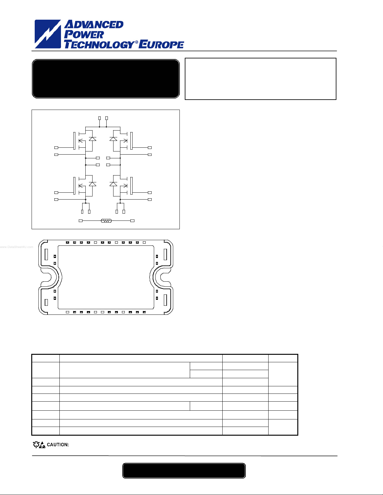
MOSFET Power Module
18
19
26
27
29
30
31
32
All multiple inputs and outputs must be shorted together
ull - Bridge
1413
Q1 Q3
7
22
23
Q2
29
15
28 27 26
2254
3
8
30
Example: 13/14 ; 29/30 ; 22/23 …
Q4
32
31
R1
87
16
182023 22
19
11
10
12
11
10
4
3
16
15
14
13
Absolute maximum ratings
ymbol Parameter Max ratings Unit
V
Drain - Source Breakdown Voltage 1200 V
DSS
ID Continuo us Drain Curre nt
IDM Pulsed Drain current 68
VGS Gate - Source Voltage ±30 V
R
Drain - Source ON Resistance 570
DSon
PD Maximum Power Dissipation Tc = 25°C 390 W
IAR Avalanche current (repetitive and non repetitive) 22 A
EAR Repetitive Avalanche Energy 50
EAS Single Pulse Avalanche Energy 3000
These Devices are sensitive to Electrostatic Discharge. Proper Handing Procedures Should Be Followed.
V
R
I
= 1200V
DSS
DSon
= 17A @ Tc = 25°C
D
Application
• Welding converters
• Switched Mode Power Supplies
• Uninterruptible Power Supplies
• Motor control
Features
• Power MOS 7® FREDFETs
• Kelvin source for easy drive
• Very low stray inductance
• Internal thermistor for temperature monitoring
• High level of integration
Benefits
• Outsta ndi ng performa nce at hi gh freq ue nc y operation
• Direct mounting to heatsink (isolated package)
• Low junction to case thermal resistance
• Solderable terminals both for power and signal for
easy PCB mounting
• Low profile
• Each leg can be easily paralleled to achieve a phase
leg of twice the current capability
Tc = 25°C 17
Tc = 80°C 13
= 570mΩ max @ Tj = 25°C
- Low R
- Low input and Miller capacitance
- Low gate char ge
- Fast intrinsic reverse diode
- Avalanche energy rated
- Very rugged
- Symme trical design
DSon
A
mΩ
mJ
, 2004
Rev 0 Septembe
APT website – http://www.advancedpower.com 1
APTM120H57FT3
6

APTM120H57FT3
–
r
–
All ratings @ Tj = 25°C unless otherwise specified
Electrical Characteristics
Symbol Characteristic Test Conditions Min Typ Max Unit
BV
Drain - Source Breakdown Voltage VGS = 0V, ID = 250µA 1200 V
DSS
I
Zero Gate Voltage Drain Current
DSS
R
Drain – Source on Resistance VGS = 10V, ID = 8.5A
DS(on)
V
Gate Threshold Voltage VGS = VDS, ID = 2.5mA 3 5 V
GS(th )
I
Gate – Source Leakage Current VGS = ±30 V, VDS = 0V ±100 nA
GS S
Dynamic Characteristics
Symbol Characteristic Test Conditions Min Typ Max Unit
C
Input Capacitance 5155
is s
C
Output Capacitance 770
oss
C
Reverse Transfer Capacitance
rss
Qg Total gate Charge 187
Qgs Gate – Source Charge 24
Qgd Gate – Drain Charge
T
Tur n-on Del a y Ti me 20
d(on)
T
Rise Time 15
r
T
Turn-off Delay Time 160
d(off)
T
Fall Time
f
E
Tur n-on Sw itchi ng Energy X 990
on
E
Turn-off Switching Energy Y
off
VGS = 0V,VDS = 1200V Tj = 25°C 100
VGS = 0V,VDS = 1000V Tj = 125°C 500
570
µA
mΩ
VGS = 0V
VDS = 25V
f = 1MHz
130
pF
VGS = 10V
V
= 600V
Bus
ID = 17A
120
nC
Inductive switching @ 125°C
VGS = 15V
V
= 800V
Bus
ns
ID = 17A
RG = 5Ω
45
Inductive switching @ 25°C
VGS = 15V, V
= 800V
Bus
µJ
ID = 17A, RG = 5Ω 685
E
Tur n-on Sw itchi ng Energy X 1565
on
E
Turn-off Switching Energy Y
off
Inductive switching @ 125°C
VGS = 15V, V
= 800V
Bus
ID = 17A, RG = 5Ω
µJ
857
Source - Drain diode ratings and characteristics
Symbol Characteristic Test Conditions Min Typ Max Unit
(Body diode)
Tc = 25°C 17 IS Conti nuo us Source c urre nt
Tc = 80°C 13
A
VSD Diode Forward Voltage VGS = 0V, IS = - 17A 1.3 V
dv/dt Peak Diode Recovery Z 18 V/ns
trr Reverse Recovery Time
Qrr Reverse Recovery Charge
IS = - 17A
VR = 600V
diS/dt = 100A/µs
IS = - 17A
VR = 600V
diS/dt = 100A/µs
Tj = 25°C 320
Tj = 125°C 650
Tj = 25°C 2
Tj = 125°C 7
ns
µC
, 2004
X Eon includes diode reverse recovery.
Y In accordance with JEDEC standard JESD24-1.
Z dv/dt numbers reflect the li mitations of the circuit rather than the device itself.
IS ≤ - 17A di/dt ≤ 700A/µs VR ≤ V
Tj ≤ 150°C
DSS
Rev 0 Septembe
APT website – http://www.advancedpower.com 2
APTM120H57FT3
6

APTM120H57FT3
–
r
–
Thermal and package characteristics
Symbol Characteristic Min Typ Max Unit
R
Junction to Case 0.32 °C/W
thJC
V
TJ Operating junction temperature range
T
TC Operating Case Temperature -40 100
Torque Mounting torque To heatsink M4 4.7 N.m
Wt Package Weight 110 g
Temperature sensor NTC
Symbol Characteristic Min Typ Max Unit
R25 Resistance @ 25°C
B
25/85
Package outline
RMS Isolation Voltage, any terminal to case t =1 min, I isol<1mA, 50/60Hz
ISOL
2500 V
-40 150
Storage Temperature Range -40 125
STG
68
T
= 298.16 K 4080 K
25
R
=
R
T
exp
25
B
85/25
25
T: Thermis tor temperat ure
11
−
RT: Thermistor value at T
TT
°C
kΩ
28
1
17
, 2004
12
Rev 0 Septembe
APT website – http://www.advancedpower.com 3
APTM120H57FT3
6

–
r
–
Typical Performance Curve
Maximum Effective Transient Thermal Impedance, Junction to Case vs Pulse Duration
0.35
0.3
0.9
APTM120H57FT3
0.25
0.2
0.7
0.5
0.15
0.1
0.05
Thermal Impedance (°C/W)
0.3
0.1
0.05
0
Single Pulse
0.00001 0.0001 0.001 0.01 0.1 1 10
rectangular Pulse Duration (Seconds)
Low Voltage Output Characteristics
50
VGS=15, 10 & 8V
40
30
7V
6.5V
80
70
60
50
Transfert Characteristics
VDS > ID(on)xRDS(on)MAX
250µs pulse test @ < 0.5 duty cycle
40
20
, Drain Curr ent (A)
D
10
I
0
0 5 10 15 20 25 30
, Drain to Source Voltage (V)
V
DS
6V
5.5 V
5V
30
20
, Drain Current (A)
D
I
10
TJ=25°C
TJ=125°C
TJ=-55° C
0
0123456789
V
, Gate to Source Voltage (V)
GS
DC Drain Current vs Case Temperature
20
16
12
1.4
1.3
1.2
R
DS(on)
Normalized to
V
=10V @ 8.5A
GS
vs Drain Current
VGS=10V
1.1
1
VGS=20V
0.9
0.8
0 10203040
(on) Drain to Source ON Resistance
DS
R
I
, Drain Current (A)
D
8
4
, DC Drain Current (A)
D
I
0
25 50 75 100 125 150
, Case Temperature (°C)
T
C
, 2004
Rev 0 Septembe
APT website – http://www.advancedpower.com 4
APTM120H57FT3
6

APTM120H57FT3
–
r
–
, Drain to Source Breakdown
DSS
BV
(TH), Threshold Voltage
GS
V
Breakdown Voltage vs Temperature
1.15
1.10
1.05
1.00
0.95
0.90
Voltage (Normalized)
0.85
-50 -25 0 25 50 75 100 125 150
T
, Junction Temperature (°C)
J
Threshold Voltage vs Temperature
1.2
1.1
1.0
0.9
0.8
(Normalized)
0.7
0.6
-50 -25 0 25 50 75 100 125 150
T
, Case Temperature (°C)
C
2.5
VGS=10V
=8.5A
I
D
2.0
1.5
1.0
(Normalized)
0.5
ON resistance vs Temperature
0.0
(on), Drain to Source ON resistance
DS
-50 -25 0 25 50 75 100 125 150
R
, Junction Temperature (°C)
T
J
Maximum Safe Operating Area
100
limited by RDSon
10
, Drain Current (A)
D
I
Single pulse
T
=150°C
J
1
1 10 100 1000
, Drain to Source Voltage (V)
V
DS
100µs
1ms
10m s
1200
Capacitance vs Drain to Source Voltage
100000
10000
1000
C, Capacitance (pF)
100
0 1020304050
, Drain to Source Voltage (V)
V
DS
Ciss
Coss
Crss
Gate Charge vs Gate to Source Voltage
14
12
10
ID=17A
T
=25°C
J
VDS=240V
VDS=600V
8
6
4
2
, Gate to Source Voltage (V)
GS
V
0
0 40 80 120 160 200 240
Gate Charge (nC)
VDS=960V
, 2004
Rev 0 Septembe
APT website – http://www.advancedpower.com 5
APTM120H57FT3
6

APTM120H57FT3
–
r
–
Delay Times vs Current
180
160
140
(ns)
120
100
80
60
40
VDS=800V
=5Ω
R
G
=125°C
T
J
L=100µH
d(off)
and t
d(on)
t
20
0
5 1015 20253035
, Drain Current (A)
I
D
Switching Energy vs Current
3
2.5
2
VDS=800V
=5Ω
R
G
=125°C
T
J
L=100µH
E
on
E
1.5
1
0.5
Switching Energy (mJ)
0
5 10152025 3035
ID, Drain Current (A)
t
d(on)
off
t
d(off)
80
Rise and Fall times vs Current
VDS=800V
=5Ω
R
G
=125°C
T
J
60
L=100µH
(ns)
f
40
and t
r
t
t
f
t
r
20
0
5 101520253035
, Drain Current (A)
I
D
Switching Energy vs Gate Resistance
4
3
2
VDS=800V
=17A
I
D
=125°C
T
J
L=100µH
E
off
E
on
1
Switching Energy (mJ)
0
0 5 10 15 20 25 30 35
Gate Resistance (Ohms)
Operating Frequency vs Drain Current
225
Source to Drain Diode Forward Voltage
1000
200
175
150
125
100
VDS=800V
D=50%
75
=5Ω
R
Frequency (kHz)
G
50
=125°C
T
J
25
=75°C
T
C
ZCS
ZVS
Hard
switching
0
4 6 8 10121416
, Drain Current (A)
I
D
100
TJ=150°C
10
, Reverse Drain Current (A)
DR
I
1
TJ=25°C
0.2 0.4 0.6 0.8 1 1.2 1.4 1.6 1.8
, Source to Drain Voltage (V)
V
SD
APT re se rves the rig ht to cha nge, witho ut not ice , t he s pe c ifica tio ns and i nfo rmatio n c o nta ine d he re in
APT's products are covered by one or more of U.S patents 4,895,810 5,045,903 5,089,434 5,182,234 5,019,522
5,262,336 6,503,786 5,256,583 4,748,103 5,283,202 5,231,474 5,434,095 5,528,058 and foreign patents. U.S and Foreign patents pending. All Rights Reserved.
, 2004
Rev 0 Septembe
APT website – http://www.advancedpower.com 6
APTM120H57FT3
6
 Loading...