

查询APT15GP60BDF1供应商
APT15GP60BDF1
600V
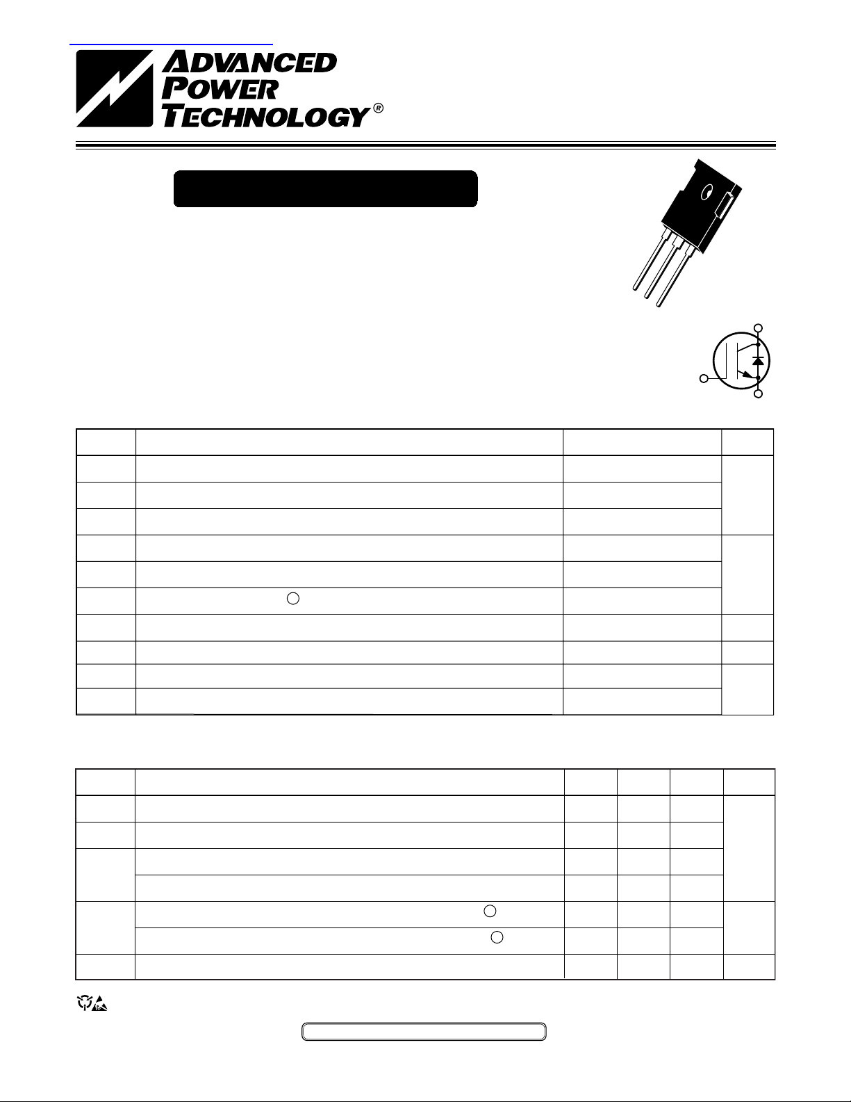
POWER MOS 7® IGBT
TO-247
The POWER MOS 7® IGBT is a new generation of high voltage power IGBTs.
Using Punch Through Technology this IGBT is ideal for many high frequency,
high voltage switching applications and has been optimized for high frequency
switchmode power supplies.
• Low Conduction Loss •100 kHz operation @ 400V, 19A
• Low Gate Charge •200 kHz operation @ 400V, 12A
• Ultrafast Tail Current shutoff •SSOA rated
MAXIMUM RATINGS All Ratings: TC = 25°C unless otherwise specified.
Symbol
Parameter
G
C
E
APT15GP60BDF1
G
UNIT
C
E
V
CES
V
GE
V
GEM
I
C1
I
C2
I
CM
SSOA
P
TJ,T
T
Collector-Emitter Voltage
Gate-Emitter Voltage
Gate-Emitter Voltage Transient
Continuous Collector Current @ T
Continuous Collector Current @ TC = 110°C
Pulsed Collector Current 1 @ TC = 25°C
Switching Safe Operating Area @ TJ = 150°C
Total Power Dissipation
D
Operating and Storage Junction Temperature Range
STG
Max. Lead Temp. for Soldering: 0.063" from Case for 10 Sec.
L
C
STATIC ELECTRICAL CHARACTERISTICS
Symbol
BV
V
GE(TH)
V
CE(ON)
I
CES
Characteristic / Test Conditions
Collector-Emitter Breakdown Voltage (V
CES
Gate Threshold Voltage (VCE = VGE, IC = 1mA, Tj = 25°C)
Collector-Emitter On Voltage (V
Collector-Emitter On Voltage (VGE = 15V, IC = 15A, Tj = 125°C)
Collector Cut-off Current (VCE = 600V, VGE = 0V, Tj = 25°C)
Collector Cut-off Current (VCE = 600V, VGE = 0V, Tj = 125°C)
= 15V, IC = 15A, Tj = 25°C)
GE
= 25°C
GE
= 0V, IC = 500µA)
600
±20
Volts
±30
56
27
Amps
65
65A @ 600V
250
-55 to 150
Watts
°C
300
MIN TYP MAX
UNIT
600
3 4.5 6
Volts
2.2 2.7
2.1
2
2
500
3000
µA
I
GES
Gate-Emitter Leakage Current (VGE = ±20V)
CAUTION: These Devices are Sensitive to Electrostatic Discharge. Proper Handling Procedures Should Be Followed.
APT Website - http://www.advancedpower.com
±100
nA
050-7428 Rev B 4-2003
DYNAMIC CHARACTERISTICS
APT15GP60BDF1
1
Symbol
C
C
oes
C
res
V
GEP
Q
Q
Q
SSOA
Characteristic
Input Capacitance
ies
Output Capacitance
Reverse Transfer Capacitance
Gate-to-Emitter Plateau Voltage
Total Gate Charge
g
Gate-Emitter Charge
ge
Gate-Collector ("Miller ") Charge
gc
Switching Safe Operating Area
3
TJ = 150°C, R
15V, L = 100µH,V
t
d(on)
t
d(off)
E
E
E
t
d(on)
t
d(off)
E
E
E
t
t
on1
on2
t
t
on1
on2
Turn-on Delay Time
Current Rise Time
r
Turn-off Delay Time
Current Fall Time
f
Turn-on Switching Energy
Turn-on Switching Energy (Diode)
Turn-off Switching Energy
off
Turn-on Delay Time
Current Rise Time
r
Turn-off Delay Time
Current Fall Time
f
Turn-on Switching Energy
Turn-on Switching Energy (Diode)
Turn-off Switching Energy
off
Inductive Switching (25°C)
4
5
6
Inductive Switching (125°C)
4 4
55
66
THERMAL AND MECHANICAL CHARACTERISTICS
Symbol
R
ΘJC
R
ΘJC
W
Characteristic
Junction to Case (IGBT)
Junction to Case (DIODE)
Package Weight
T
Test Conditions
Capacitance
= 0V, V
V
GE
CE
f = 1 MHz
Gate Charge
= 15V
V
GE
V
= 300V
CE
I
= 15A
C
= 5Ω, V
G
V
= 400V
CC
V
= 15V
GE
I
= 15A
C
R
= 5Ω
G
T
= +25°C
J
V
= 400V
CC
V
= 15V
GE
I
= 15A
C
R
= 5Ω
G
T
= +125°C
J
= 25V
= 600V
CE
GE
MIN TYP MAX
1685
=
65
MIN TYP MAX
210
15
7.5
55
12
15
8
12
29
58
130
152
121
8
12
69
88
130
267
268
.50
1.31
5.90
UNIT
pF
V
nC
A
ns
µJ
ns
µJ
UNIT
°C/W
gm
1 Repetitive Rating: Pulse width limited by maximum junction temperature.
2 For Combi devices, I
3 See MIL-STD-750 Method 3471.
4E
is the clamped inductive turn-on-energy of the IGBT only, without the effect of a commutating diode reverse recovery current
on1
adding to the IGBT turn-on loss. (See Figure 24.)
5E
is the clamped inductive turn-on energy that includes a commutating diode reverse recovery current in the IGBT turn-on switching
on2
loss. A Combi device is used for the clamping diode as shown in the E
6E
is the clamped inductive turn-off energy measured in accordance with JEDEC standard JESD24-1. (See Figures 21, 23.)
off
APT Reserves the right to change, without notice, the specifications and information contained herein.
050-7428 Rev B 4-2003
includes both IGBT and FRED leakages
ces
on2
test circuit. (See Figures 21, 22.)
TYPICAL PERFORMANCE CURVES
30
VGE = 15V.
250µs PULSE TEST
<0.5 % DUTY CYCLE
25
30
VGE = 10V.
250µs PULSE TEST
<0.5 % DUTY CYCLE
25
APT15GP60BDF1
20
15
TC=125°C
TC=25°C
TJ = -55°C
TC=-55°C
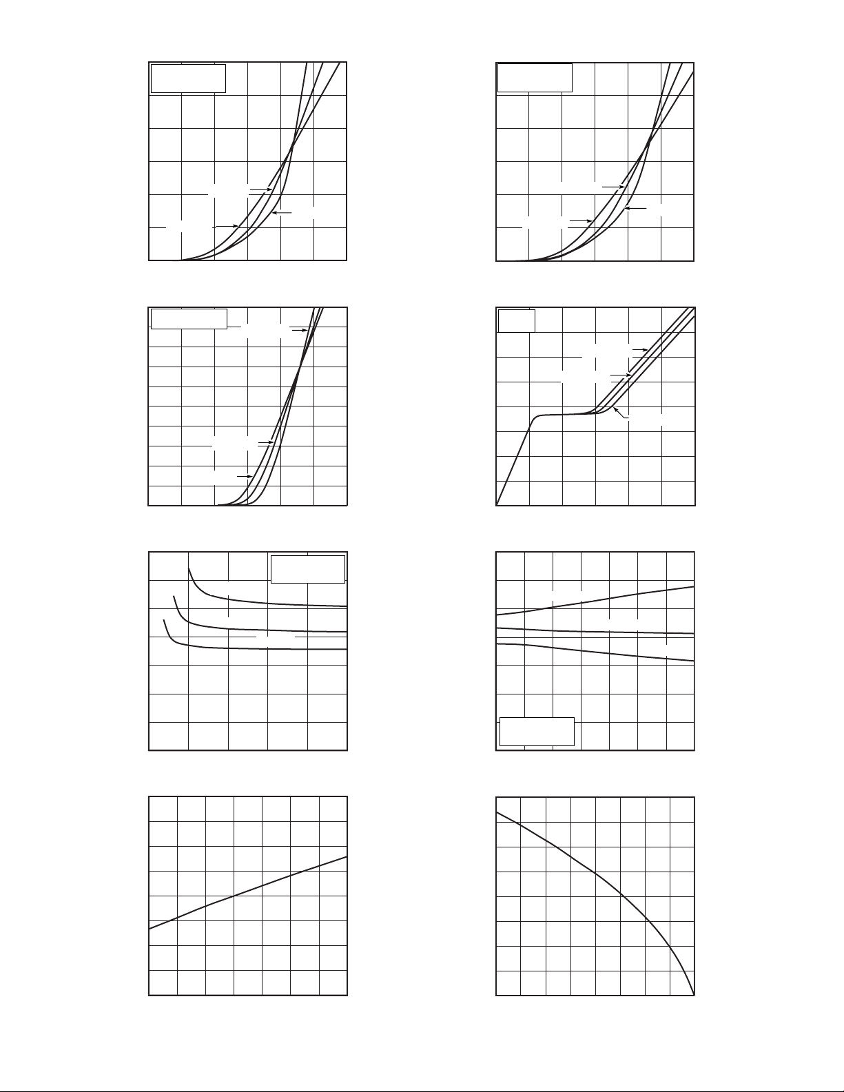
= 15V) FIGURE 2, Output Characteristics (V
GE
10
, COLLECTOR CURRENT (A)
C
5
0
0 0.5 1 1.5 2 2.5 3 0 0.5 1 1.5 2 2.5 3
VCE, COLLECTER-TO-EMITTER VOLTAGE (V) VCE, COLLECTER-TO-EMITTER VOLTAGE (V)
FIGURE 1, Output Characteristics(V
100
250µs PULSE TEST
<0.5 % DUTY CYCLE
80
60
20
15
10
, COLLECTOR CURRENT (A)
C
5
TC=25°C
TC=125°C
0
16
IC = 15A
TJ = 25°C
14
12
10
V
CE
V
CE
= 300V
= 120V
8
40
6
TJ = 25°C
, COLLECTOR CURRENT (A) I
20
C
0
TJ = 125°C
0 2 4 6 8 10 12 0 10 20 30 40 50 60
VGE, GATE-TO-EMITTER VOLTAGE (V) GATE CHARGE (nC)
4
, GATE-TO-EMITTER VOLTAGE (V) I
2
GE
0
FIGURE 3, Transfer Characteristics FIGURE 4, Gate Charge
3.5
2.5
1.5
TJ = 25°C.
250µs PULSE TEST
3
IC = 7.5A
<0.5 % DUTY CYCLE
IC =30A
2
IC = 15A
3.5
3
IC =30A
2.5
IC = 15A
2
1.5
V
CE
IC = 7.5A
TC=-55°C
= 10V)
GE
= 480V
1
0.5
, COLLECTOR-TO-EMITTER VOLTAGE (V) I
CE
0
6 8 10 12 14 16 -50 -25 0 25 50 75 100 125
VGE, GATE-TO-EMITTER VOLTAGE (V) TJ, Junction Temperature (°C)
0.5
, COLLECTOR-TO-EMITTER VOLTAGE (V) V
CE
1
VGE = 15V.
250µs PULSE TEST
<0.5 % DUTY CYCLE
0
FIGURE 5, On State Voltage vs Gate-to- Emitter Voltage FIGURE 6, On State Voltage vs Junction Temperature
1.2
1.15
1.10
1.05
1.0
0.95
0.9
VOLTAGE (NORMALIZED)
0.85
, COLLECTOR-TO-EMITTER BREAKDOWN V
CES
0.8
-50 -25 0 25 50 75 100 125 -50 -25 0 25 50 75 100 125 150
BV
FIGURE 7, Breakdown Voltage vs. Junction Temperature FIGURE 8, DC Collector Current vs Case Temperature
T
, JUNCTION TEMPERATURE (°C) TC, CASE TEMPERATURE (°C)
J
80
70
60
50
40
30
20
DC COLLECTOR CURRENT(A) V
C,
I
10
0
050-7428 Rev B 4-2003

18
16
14
VGE= 10V
12
VGE= 15V
80
V
=15V,T
70
60
V
=10V,T
=125°C
J
GE
GE
50
10
40
V
=15V,T
=25°C
J
8
6
, TURN-ON DELAY TIME (ns)
4
d(ON)
2
0
5 10 15 20 25 30 5 10 15 20 25 30
ICE, COLLECTOR TO EMITTER CURRENT (A) ICE, COLLECTOR TO EMITTER CURRENT (A)
V
= 400V
CE
= 25°C or 125°C
T
J
RG = 5Ω
L = 100 µH
, TURN-OFF DELAY TIME (ns)
(OFF)
d
30
20
10
0
GE
V
= 400V
CE
= 5Ω
R
G
L = 100 µH
V
=10V,T
GE
FIGURE 9, Turn-On Delay Time vs Collector Current FIGURE 10, Turn-Off Delay Time vs Collector Current
30
T
= 25 or 125°C,V
25
J
GE
= 10V
20
100
80
T
= 125°C, VGE = 10V
J
60
15
RISE TIME (ns) t
r,
10
40
FALL TIME (ns) t
f,
T
= 25°C, VGE = 10V
J
or 15V
APT15GP60BDF1
=125°C
J
=25°C
J
or 15V
T
= 25 or 125°C,V
5
0
5 10 15 20 25 30 5 10 15 20 25 30
I
, COLLECTOR TO EMITTER CURRENT (A) ICE, COLLECTOR TO EMITTER CURRENT (A)
CE
FIGURE 11, Current Rise Time vs Collector Current FIGURE 12, Current Fall Time vs Collector Current
700
VCE = 400V
L = 100 µH
RG = 5 Ω
600
500
J
R
G
TJ =125°C,VGE=10V
=5Ω, L = 100µH, V
400
300
200
, TURN ON ENERGY LOSS (µJ) t
ON2
100
TJ = 25°C, VGE=10V
0
0 5 10 15 20 25 30 5 10 15 20 25 30
I
, COLLECTOR TO EMITTER CURRENT (A) ICE, COLLECTOR TO EMITTER CURRENT (A)
CE
FIGURE 13, Turn-On Energy Loss vs Collector Current FIGURE 14, Turn Off Energy Loss vs Collector Current
900
VCE = 400V
VGE = +15V
800
TJ = 125°C
= 15V
GE
CE
TJ =125°C, VGE=15V
TJ = 25°C, VGE=15V
E
30A
on2
= 400V
, TURN OFF ENERGY LOSS (µJ) t
OFF
20
0
700
600
500
400
300
200
100
0
700
600
R
=5Ω, L = 100µH, V
G
VCE = 400V
L = 100 µH
RG = 5 Ω
VCE = 400V
VGE = +15V
RG = 5 Ω
= 400V
CE
T
= 125°C, VGE = 10V
J
T
= 25°C, VGE = 10V
J
or 15V
or 15V
700
E
30A
600
off
500
400
300
200
100
SWITCHING ENERGY LOSSES (µJ) E
E
15A
on2
E
15A
E
7.5A
on2
off
E
7.5A
off
0
0 10 20 30 40 5 0 -50 -25 0 25 50 75 100 125
R
, GATE RESISTANCE (OHMS) TJ, JUNCTION TEMPERATURE (°C)
FIGURE 15, Switching Energy Losses vs. Gate Resistance FIGURE 16, Switching Energy Losses vs Junction Temperature
G
500
E
30A
on2
400
E
30A
off
300
200
E
15A
on2
E
100
SWITCHING ENERGY LOSSES (µJ) E
15A
off
E
7.5A
on2
E
7.5A
off
0
050-7428 Rev B 4-2003

TYPICAL PERFORMANCE CURVES
Note:
Duty Factor D =
t
1
/
t
2
Peak TJ = PDM x Z
θJC
+ T
C
t
1
t
2
P
DM
d( on ) r d( off ) f
tttt
0
4,000
1,000
F)
500
P
100
50
C, CAPACITANCE (
70
C
ies
60
APT15GP60BDF1
50
40
C
oes
30
, COLLECTOR CURRENT (A)
20
C
I
C
res
10
10
0 10 20 30 40 5 0 0 100 200 300 400 500 600 700
VCE, COLLECTOR-TO-EMITTER VOLTAGE (VOLTS) VCE, COLLECTOR TO EMITTER VOLTAGE
Figure 17, Capacitance vs Collector-To-Emitter Voltage Figure 18, Minimim Switching Safe Operating Area
0.60
0.50
0.9
0.40
0.7
0.30
0.20
, THERMAL IMPEDANCE (°C/W)
0.10
JC
θ
Z
0
-5
10
0.5
0.3
0.1
0.05
SINGLE PULSE
-4
10
Figure 19A, Maximum Effective Transient Thermal Impedance, Junction-To-Case vs Pulse Duration
RC MODEL
Junction
temp. ( ”C)
0.216
0.0060
Power
(Watts)
0.284
0.164
Case temperature
FIGURE 19B, TRANSIENT THERMAL IMPEDANCE MODEL
0
-3
10
-2
10
RECTANGULAR PULSE DURATION (SECONDS)
292
100
50
TJ = 125°C
TC = 75°C
, OPERATING FREQUENCY (kHz)
D = 50 %
VCE = 400V
MAX
F
RG = 5 Ω
10
5101520253035404550
IC, COLLECTOR CURRENT (A)
Figure 20, Operating Frequency vs Collector Current
-1
10
1.0
Fmin(f,f)
=
max max1 max 2
f
=
max1
f
=
max2
P
=
diss
0.05
++ +
PP
−
diss cond
EE
+
on2 off
TT
−
JC
R
θ
JC
050-7428 Rev B 4-2003

APT15GP60BDF1
*DRIVER SAME TYPE AS D.U.T.
I
C
V
CLAMP
100uH
V
TEST
A
A
B
D.U.T.
DRIVER*
V
CE
Figure 24, E
ON1
Test Circuit
V
V
I
CE
CC
Figure 21, Inductive Switching Test Circuit
C
D.U.T.
90%
t
d(off)
t
f
90%
APT15DF60
A
Gate Voltage
Collector Voltage
T
TJ = 125 C
Gate Voltage
10%
t
d(on)
t
r
Collector Current
90%
10%
5%
Switching Energy
Figure 22, Turn-on Switching Waveforms and Definitions
5 %
Collector Voltage
TJ = 125 C
10%
Switching Energy
Figure 23, Turn-off Switching Waveforms and Definitions
Collector Current
0
050-7428 Rev B 4-2003

TYPICAL PERFORMANCE CURVES
Note:
Duty Factor D =
t
1
/
t
2
Peak TJ = PDM x Z
θJC
+ T
C
t
1
t
2
P
DM
APT15GP60BDF1
ULTRAFAST SOFT RECOVERY ANTI-PARALLEL DIODE
MAXIMUM RATINGS All Ratings: TC = 25°C unless otherwise specified.
Symbol
(AV)
I
F
IF(RMS)
I
FSM
Characteristic / Test Conditions
Maximum Average Forward Current (T
RMS Forward Current
Non-Repetitive Forward Surge Current (T
STATIC ELECTRICAL CHARACTERISTICS
Symbol
V
Characteristic / Test Conditions
Forward Voltage I
F
DYNAMIC CHARACTERISTICS
= 94°C, Duty Cycle = 0.5)
C
= 45°C, 8.3ms)
J
= 15A
I
F
= 30A
F
IF = 15A, TJ = 150°C
APT15GP60BDF1
15
36
110
MIN TYP MAX
2.2
2.7
1.6
UNIT
Amps
UNIT
Volts
Symbol
t
rr1
t
rr2
t
fr1
t
fr2
I
RRM1
I
RRM2
Q
rr1
Q
rr2
V
fr1
V
fr2
Characteristic
Reverse Recovery Time T
= 25°C
J
IF = 15A, diF/dt = -200A/µs, VR = 400V TJ = 100°C
Forward Recovery Time TJ = 25°C
= 15A, diF/dt = 200A/µs, VR = 400V TJ = 100°C
I
F
Maximum Reverse Recovery Current TJ = 25°C
= 15A, diF/dt = -200A/µs, VR = 400V TJ = 100°C
I
F
Reverse Recovery Charge T
= 25°C
J
IF = 15A, diF/dt = -200A/µs, VR = 400V TJ = 100°C
Forward Recovery Voltage T
= 25°C
J
IF = 15A, diF/dt = 200A/µs, VR = 400V TJ = 100°C
1.4
1.2
1.0
0.8
0.6
0.9
0.7
0.5
MIN TYP MAX
56
58
106
106
2.3
6
77
235
5
5
UNIT
ns
Amps
nC
Volts
0.4
, THERMAL IMPEDANCE (°C/W)
JC
θ
Z
0.2
0
0.3
0.1
0.05
-5
10
FIGURE 25. MAXIMUM EFFECTIVE TRANSIENT THERMAL IMPEDANCE, JUNCTION-TO-CASE vs PULSE DURATION
-4
10
SINGLE PULSE
-3
10
RECTANGULAR PULSE DURATION (seconds)
-2
10
-1
10
1.0
050-7428 Rev B 4-2003

100
80
60
TJ = 175°C
TJ = 100°C
40
, FORWARD CURRENT
F
20
0
Figure 26, Forward Voltage vs. Forward Current Figure 27, Reverse Recovery Charge vs. Current Rate of Decrease
16
14
TJ = 150°C
TJ = 25°C
0 1 2 3 4 5 0 200 400 600 800 1000
V
, ANODE-TO-CATHODE VOLTAGE (V) diF/dt, CURRENT RATE OF DECREASE(A/ µs)
F
TJ=100°C
V
R
=400V
30A
500
TJ=100°C
450
VR=400V
400
30A
350
300
250
200
150
100
, REVERSE RECOVERY CHARGE
rr
50
0
1.6
1.4
7.5A
Q
15A
rr
APT15GP60BDF1
12
10
15A
8
6
7.5A
4
, REVERSE RECOVERY CURRENT I
RRM
Figure 28, Reverse Recovery Current vs. Current Rate of Decrease Figure 29, Dynamic Parameters vs. Junction Temperature
2
0
0 200 400 600 800 1000 0 25 50 75 100 125 150
di
/dt, CURRENT RATE OF DECREASE (A/µs) TJ, JUNCTION TEMPERATURE (°C)
F
100
TJ=100°C
VR=350V
80
30A
60
15A
7.5A
40
1.2
I
RRM
1.0
t
rr
0.8
0.6
0.4
, DYNAMIC PARAMETERS Q
f
0.2
0.0
30
25
20
15
(ns) (NORMALIZED) (nC)
10
, REVERSE RECOVERY TIME I
Figure 30, Reverse Recovery Time vs. Current Rate of Decrease Figure 31, Forward Recovery Voltage/Time vs. Current Rate of Decrease
20
rr
0
0 200 400 600 800 1000 0 200 400 600 800 1000
di
/dt, CURRENT RATE OF DECREASEs (A/µs) diF/dt, CURRENT RATE OF DECREASE (A/ µs)
F
, FORWARD RECOVERY TIME K
fr
250
30
5
0
TJ=100°C
VR=400V
IF=15A
t
rr
Q
rr
120
V
fr
100
80
60
t
fr
40
20
0
(V)
, FORWARD RECOVERY VOLTAGE
fr
V
200
25
20
150
(A) t
(pF) (ns) (A) (A)
100
, JUNCTION CAPACITANCE t
C
VR, REVERSE VOLTAGE (V) Case Temperature (°C)
50
J
0
.3 1 10 100 200 25 50 75 100 125 150
I
F(AV)
15
10
5
0
Figure 32, Junction Capacitance vs. Reverse Voltage Figure 33, Maximum Average Forward Current vs.
CaseTemperature
050-7428 Rev B 4-2003

30µH
APT15GP60BDF1
V
r
D.U.T.
t
Q
/
rr
rr
Waveform
+15v
diF/dt Adjust
0v
-15v
Figure 10. Diode Reverse Recovery Test Circuit and Waveforms
I
1
- Forward Conduction Current
F
di
2
/dt - Current Rate of Decrease, Rate of Diode
F
Current Change Through Zero Crossing
From Positive to Negative.
3
I
- Maximum Reverse Recovery Current.
RRM
4
trr - Reverse
R
ecovery Time, measured from zero crossing where diode
current goes from positive to negative, to the point at which the straight
line through I
5
Qrr - Area Under the Curve Defined by I
6
/dt - Maximum Rate of Current Increase During the Trailing Portion of t
di
M
Junction
temp. ( ”C)
and 0.25 I
RRM
RC MODEL
0.698
passes through zero.
RRM
and trr.
RRM
0.00173F
Zero
PEARSON 2878
CURRENT
TRANSFORMER
1
4
5
3
0.25 I
Slope = diM/
6
RRM
dt
2
rr.
Power
(Watts)
Case temperature
0.438
0.165
0.0395F
0.670F
TRANSIENT THERMAL IMPEDANCE MODEL
T0-247 Package Outline
4.69 (.185)
5.31 (.209)
1.49 (.059)
2.49 (.098)
6.15 (.242) BSC
20.80 (.819)
21.46 (.845)
Collector
(Cathode)
4.50 (.177) Max.
0.40 (.016)
0.79 (.031)
2.21 (.087)
2.59 (.102)
APT’s products are covered by one or more of U.S.patents 4,895,810 5,045,903 5,089,434 5,182,234 5,019,522
5,262,336 6,503,786 5,256,583 4,748,103 5,283,202 5,231,474 5,434,095 5,528,058 and foreign patents. US and Foreign patents pending. All Rights Reserved.
19.81 (.780)
20.32 (.800)
1.01 (.040)
1.40 (.055)
5.45 (.215) BSC
Dimensions in Millimeters and (Inches)
2-Plcs.
15.49 (.610)
16.26 (.640)
5.38 (.212)
6.20 (.244)
3.55 (.138)
3.81 (.150)
2.87 (.113)
3.12 (.123)
1.65 (.065)
2.13 (.084)
Gate
Collector
(Cathode)
Emitter
(Anode)
050-7428 Rev B 4-2003
 Loading...